Study on Structural, Optical and Electrical
Properties of CuScO2 Thin Films as p-type
Transparent Oxide Semiconductors
著者
Kakehi Yoshiharu
内容記述
学位授与大学: Osaka Prefecture University(大阪
府立大学), 学位の種類: 博士(工学), 学位記番号:
論工第1230号, 学位授与年月日: 2009-12-20, 指導
教員: 藤村紀文
権利
Journal of the Vacuum Society of Japan.
vol.46, p.473-477(2003), vol.47,
p.265-268(2004). 日本真空協会
Thin Solid Films. vol.445, p.294-298(2003),
vol.516, p.5785-5789(2008), vol.518,
p.3097-3100(2010). Elsevier
Journal of Crystal Growth. vol.311,
p.1117-1122(2009). Elsevier
Vacuum. vol.84, p.618-621(2010). Elsevier
Journal of Applied Physics. vol.97,
p.083535-1-083535-6(2005). AIP
Japanese Journal of Applied Physics. v.46,
p.4228-4232(2007). 応用物理学会
Study on Structural, Optical and Electrical Properties of
CuScO
2Thin Films
as p-type Transparent Oxide Semiconductors
Yoshiharu Kakehi
November 2009
Table of Contents
Chapter 1. General Introduction
1Chapter 2. Crystallographic Analysis of CuScO
2Thin Films
Deposited on A-plane Sapphire Substrates
2.1Introduction 14 2.2Experimental 14 2.3 Results and Discussion
2.3.1 Thermal decomposition reaction of Cu2Sc2O5 bulk 21
2.3.2 Substrate temperature dependence of film quality 21 2.3.3 Oxygen pressure dependence of film quality 29 2.3.4 Fabrication of CuScO2(0001) epitaxial films and the effect of
laser fluence on the in-plane orientation of the epitaxial films 35 2.3.5 Chemical composition and optical property of
CuScO2[3R](0001) epitaxial film 52
2.4 Conclusion 52
Chapter 3. Structural, Optical and
Electrical Transport Properties of
CuScO
2[3R](0001) Epitaxial Thick Films
3.1 Introduction 57 3.2 Experimental 59 3.3 Results and Discussion
3.3.1 Effect of oxygen pressure during post-annealing treatment on
film quality of CuScO2[3R] polycrystalline thick films 62
3.3.2 Effect of laser fluence on the out-of-plane and in-plane orientations of CuScO2[3R] polycrystalline thick films 70
3.3.3 Fabrication of CuScO2[3R](0001) epitaxial thick films using
3.3.4 Optical and electrical transport properties of
CuScO2[3R](0001) epitaxial thick films 81
3.4 Conclusion 84
Chapter 4. Structural, Optical and
Electrical Transport Properties of
CuScO
2[3R](0001) Epitaxial Films
Intercalated with Excess Oxygen
4.1 Introduction 86 4.2 Experimental 86 4.3 Results and Discussion
4.3.1 Structural property of CuScO2[3R](0001) epitaxial films
intercalated with excess oxygen 89 4.3.2 Optical property of CuScO2[3R](0001) epitaxial films
intercalated with excess oxygen 89 4.3.3 Conduction mechanism of CuScO2[3R](0001) epitaxial films
intercalated with excess oxygen 94 4.4 Conclusion 98
Chapter 5. Effect of Mg Doping in the Sc-sites on
Structural, Optical and
Electrical Transport Properties of
CuScO
2[3R](0001) Epitaxial Thick Films
5.1 Introduction 100 5.2 Experimental 100 5.3 Results and Discussion
5.3.1 Preparation of Mg-doped CuScO2[3R](0001) epitaxial thick films 102
5.3.2 Optical and electrical transport properties of
1-at% Mg-doped CuScO2[3R](0001) epitaxial thick film 108
Chapter 6. Control of Carrier Concentration in
CuScO
2[3R](0001) Epitaxial Thick Films
through Excess Oxygen and Mg Co-doping
6.1 Introduction 114
6.2 Experimental 115
6.3 Results and Discussion 6.3.1 Control of the carrier concentration in CuScO2[3R](0001) epitaxial thick films through excess oxygen and Mg co-doping 115
6.3.2 Optical and electrical transport properties of excess oxygen and Mg co-doped CuScO2[3R](0001) epitaxial thick film 122
6.4 Conclusion 125
Chapter 7. Conclusions
128Chapter 1. General Introduction
Some wide gap oxides such as In2O3, ZnO, and SnO2 are n-type transparent oxide
semiconductors (TOSs) with unique features of high optical transparency in the visible region and controllable electrical conductivity through extrinsic doping. They can be changed to transparent conductors by higher extrinsic doping, whose electrical conductivities are almost equivalent to those of typical metals. Therefore, they are termed transparent conducting oxides and have been widely used for a long time in optoelectronics applications as well as in various research fields. The first report of a transparent conducting oxide film was published in 1907 when the first cadmium oxide films were prepared by thermally oxidizing sputtered films of cadmium [1]. Since then, extensive works have been done in the field of transparent conducting oxide technology to prepare new types of transparent conducting oxides with wide ranging applications. These include binary and ternary compounds and new materials such as Sn-doped In2O3
[2,3], B,Al,Ga,In-doped ZnO [4,5], Sb,F-doped SnO2 [6,7], Nb,Ta-doped TiO2 [8,9],
Zn2SnO4 [10-12], ZnSnO3 [13], In2O3-ZnO(IZO) [14], Cd2SnO4 [15], MgIn2O4 [16],
Zn2In2O5 [17], Sn-doped Ga2O3 [18], and 12CaO-7Al2O3 [19]. The important
applications in which transparent conducting oxides are used are transparent electrodes for solar cells and flat panel displays, low-emissivity windows, oven windows, touch-sensitive control panels, defrosting windows in refrigerators and airplanes, invisible security circuits, gas sensors, and antistatic coatings [2,20-26]. However, only a limited number of studies have been done on these materials as TOSs. This is because the above-mentioned transparent conducting oxides are n-type TOSs and there has been little possibility of realizing transparent pn-junctions essential for the electron activity of
semiconductors due to the lack of p-type TOSs.
With regard to p-type TOSs, CuAlO2 was first shown to be a p-type transparent
semiconductor by Benko and Koffyberg in 1984 [27]. A sintered pellet of CuAlO2 with
no intentional doping showed a p-type electrical conductivity of 1.7×10⁻³ Scm-1 at room temperature. Undoped CuFeO2 exhibited a p-type electrical conductivity, and
substituting 2% Mg for Fe increased p-type electrical conductivity [28]. On the other hand, substituting 5% Sn for Fe in CuFeO2 showed n-type electrical conductivity. This
indicates that the bipolar doping is achieved in CuFeO2 through extrinsic dopants [28].
CuCrO2 and CuYO2 were doping by substituting Ca for the trivalent cation [29,30].
However, the carrier concentration and Hall mobility for these pellets were not determined by Hall effect measurements probably due to very low Hall mobility. Moreover, the first report of a p-type TOS film was published in 1993 [31]. The electrical conductivity of a 110-nm-thick NiO polycrystalline film with no intentional doping was 7.1 Scm-1 at room temperature, but the transmittance of the film was as low as 40% in the visible region. Therefore, there has been considerable interest in finding new p-type TOSs.
In 1997, Kawazoe et al. argued that it was very difficult to prepare binary metallic oxides with p-type electrical conductivity because holes introduced at oxygen 2p levels were strongly localized due to the high electronegative nature of oxygen based on the electronic structure of the metallic oxides. Therefore, they showed the chemical design concept to explore new p-type TOSs called “chemical modulation of the valence band (CMVB)” to delocalize the holes introduced at oxygen 2p levels and proposed the delafossite structure (CuFeO2) as the structural requirement for designing p-type TOSs
[32]. Furthermore, they also reported that a 500-nm-thick CuAlO2+X thin film with a
(a)
(b)
(a)
(b)
Fig. 1-1 Crystal structures of (a) 2H and (b) 3R phases of Cu-based delafossites (Cu+M3+O2) with hexagonal c-axis vertical. Large spheres are Cu atoms,
and small spheres are O atoms. Orientation of MO6 octahedra is same for
electrical conductivity of 9.5×10⁻¹ Scm-1 at room temperature [32]. This has opened up a new field in transparent electronics device technology, the so-called “Transparent Electronics” or “Invisible Electronics” [33]. However, the results of the later study for CuAlO2 showed that it was very difficult to control the carrier concentration in CuAlO2
by intercalating with excess oxygen near the Cu-planes or by substituting divalent species for the octahedral Al-sites [34]. Therefore, other Cu-based delafossites isostructural with CuAlO2 have attracted much attention not only as thermoelectric,
catalytic, and luminescent materials [35-37] but also as new p-type TOSs.
Cu-based delafossites are expressed by the general formula Cu+M3+O2, and the
M3+ trivalent cation can range in size from Al to lanthanides [38]. They have two crystalline phases that depend on the stacking periods of Cu+ layers and (MO2)
-octahedral layers along the c-axis termed the 2H (hexagonal) and 3R (rhombohedral) phases, as shown in Fig. 1-1. With increasing the M3+-site ionic radius, the magnitude of the a-axis lattice constant expressed as the hexagonal system increases from 0.28567 nm to 0.38311 nm and that of the c-axis lattice constant is almost constant [39]. The Cu-Cu distances (a-axis lattice constant) have been known to significantly influence the Cu-Cu interactions, that is, electrical conductivity, because holes predominantly pass through the Cu-planes [40].
Copper-scandium oxide (CuScO2) is a p-type Cu-based delafossite. CuScO2 also
has two crystalline phases: rhombohedral (CuScO2[3R]) and hexagonal (CuScO2[2H])
[34,41,42]. The a- and c-axis lattice constants of each phase are 0.3216 nm and 1.7089 nm for CuScO2[3R] [43] and 0.3215 nm and 1.1386 nm for CuScO2[2H] [44]. Most of
the powder preparations have been reported to yield a mixture of the two phases [40]. Unlike CuAlO2 and CuGaO2, holes in CuScO2 can be introduced by intercalating with
Sc-sites [34,41,42]. CuScO2 potentially has a relatively high Hall mobility, because
CuScO2 is a Cu-based delafossite with the smallest Cu-Cu distance for which excess
oxygen intercalation near the Cu-planes is possible [41]. Consequently, CuScO2 is
expected to be a new p-type TOS with the controllable carrier concentration through extrinsic doping.
In previous studies for CuScO2, a 110-nm-thick CuScO2+X polycrystalline film
was first reported to show a maximum electrical conductivity of 30 Scm-1 at room temperature in Cu-based delafossites by Duan et al. in 2000 [45]. After that, a lot of reports have been published on the new synthesis method to obtain single-phase CuScO2[3R] and CuScO2[2H] powders [34,46], the analysis of strong negative thermal
expansion along the O-Cu-O linkage in CuScO2 [44,47], the structural and transport
properties of Mg-doped CuScO2+X polycrystalline films and pellets [34,41,42,48-50],
the interstitial oxygen site in CuScO2[3R] and CuScO2[2H] pellets intercalated with
excess oxygen [51], the electronic structure of CuScO2 and the discovery of the intense
excitonic peak [52,53], and the first principle study of extrinsic defects in CuScO2 [54].
However, the carrier concentration and Hall mobility of CuScO2 have not been
determined by Hall effect measurements using CuScO2 polycrystalline films and pellets.
This is due to the anisotropic electrical conductivity between parallel and perpendicular to the c-axis direction owing to the delafossite structure, thus CuScO2 epitaxial films
must be prepared. However, the epitaxial growth of CuScO2 thin films has not been
reported until now.
We succeeded in fabricating a 50-nm-thick CuScO2[3R](0001) epitaxial film on
an a-plane sapphire substrate using a pulsed laser deposition (PLD) method (Chapter 2). However, by increasing the film thickness using a high laser repetition frequency, grains with different orientations can easily be grown in the deposited films, as shown in Fig.
10
20
30
40
50
60
70
2θ (degree)
L
og Int
ens
it
y (a
rbi
ta
ry uni
ts
)
(a)
(b)
0003
[3 R ]0006
[3 R ]0009
[3 R ]00012
[3 R ]1011
[3 R ]2022
[3 R ]Sub
.
Sub.
Fig. 1-2 XRD 2θ-ω patterns of CuScO2 thin films prepared at different laser
repetition frequencies. Laser repetition frequency and deposition rate of each film are as follows: (a) 2 h, 1 Hz, and 25 nm h-1 (epitaxial film); and (b) 2 h, 10 Hz, and 244 nm h-1. Other deposition parameters are a substrate temperature of 925 °C, an oxygen pressure of 1.5 Pa, an rf forward power of the oxygen radical source of 200 W, and a laser fluence of 2.6 Jcm-2.
1-2. Although the deposition at a relatively high substrate temperature is very useful to solve this problem, the chemical composition of the films easily deviates due to the difference in the vapor pressure between elements during deposition in conventional vapor phase deposition methods. Therefore, a solid-phase epitaxy method was used to obtain CuScO2 epitaxial thick films. In this method, a bilayer laminate composed of a
thin epitaxial layer is grown on a single-crystal substrate and a thicker polycrystalline or amorphous layer of a target, deposited at room temperature, is thermally annealed at high temperature (> 1000 °C). The solid-state reaction at high temperature leads to the formation of a thin, single-crystalline layer on the substrate, which may work as an epitaxial template for successive homoepitaxial growth of the film [55]. This method is very effective when growing complex compounds that have both a high vapor pressure and a high melting point, because the deposition process of the film is separated from the epitaxial growth process.
In this thesis, the deposition and post-annealing conditions of CuScO2 thin films
are investigated to obtain single-phase CuScO2[3R](0001) epitaxial thick films using a
solid-phase epitaxy method. The structural, optical, and electrical transport properties of the undoped and extrinsic doped films are then discussed to obtain transparent p-type CuScO2[3R](0001) epitaxial thick films with the controllable carrier concentration
through extrinsic doping. This thesis is composed of seven chapters.
In chapter 2, CuScO2 thin films are deposited on a-plane sapphire substrates by
PLD using a single-phase Cu2Sc2O5 target. The effects of the substrate temperature,
oxygen pressure, and laser fluence on the film quality are investigated to obtain CuScO2(0001) epitaxial films to be used as thin epitaxial layers in a solid-phase epitaxy
method. The crystallographic characteristics of the deposited films are evaluated by X-ray diffraction (XRD) measurements, and the in-plane orientation relationship
(1) Preparation of CuScO2[3R](0001) epitaxial thin film by PLD
A-plane sapphire substrate
[Chapter 3]
CuScO2[3R](0001) epitaxial film
(thickness = 200 ∼ 300nm)
A-plane sapphire substrate
[Chapter 2]
CuScO2[3R](0001) epitaxial film
(thickness < 10nm)
(2) Preparation of CuScO2[3R] polycrystalline thick film by PLD
A-plane sapphire substrate
[Chapter 3]
CuScO2[3R] polycrystalline film
(thickness = 200 ∼ 300nm)
(3) Post-annealing treatment under controlling oxygen pressure
[Chapter 3]
Post-annealing treatment using electric furnace
(Oxygen pressure = 100 ∼ 1 kPa)
(4) Fabrication of CuScO2[3R](0001) epitaxial thick film
Electric furnace (Ta ≥ 1050 ° C)
(1) Preparation of CuScO2[3R](0001) epitaxial thin film by PLD
A-plane sapphire substrate
[Chapter 3]
CuScO2[3R](0001) epitaxial film
(thickness = 200 ∼ 300nm) A-plane sapphire substrate A-plane sapphire substrate [Chapter 2]
CuScO2[3R](0001) epitaxial film
(thickness < 10nm)
(2) Preparation of CuScO2[3R] polycrystalline thick film by PLD
A-plane sapphire substrate A-plane sapphire substrate [Chapter 3]
CuScO2[3R] polycrystalline film
(thickness = 200 ∼ 300nm)
(3) Post-annealing treatment under controlling oxygen pressure
[Chapter 3]
Post-annealing treatment using electric furnace
(Oxygen pressure = 100 ∼ 1 kPa)
(4) Fabrication of CuScO2[3R](0001) epitaxial thick film
Electric furnace (Ta ≥ 1050 ° C)
Fig. 1-3 Schematic illustration of fabrication of CuScO2[3R](0001) epitaxial thick
between the substrates and the films is also discussed.
Chapter 3 focuses on the fabrication of single-phase CuScO2(0001) epitaxial thick
films using a solid-phase epitaxy method. By converting CuScO2 amorphous films into
CuScO2[3R] polycrystalline films in the fabrication process, single-phase
CuScO2[3R](0001) epitaxial thick films are successfully obtained on a-plane sapphire
substrates, as shown in Fig. 1-3. The electrical transport property of the films is first estimated using Hall effect measurements.
In chapter 4, the excess oxygen intercalation is investigated as the control method of the carrier concentration in CuScO2[3R](0001) epitaxial thick films. However, a
number of holes generated by the excess oxygen intercalation exist near the film surface, thus a 40-nm-thick CuScO2[3R](0001) epitaxial film prepared using the fabrication
method described in chapter 3 is used as the sample to intercalate with excess oxygen in the whole film. The effects of the excess oxygen intercalation on the structural, optical, and electrical transport properties of the film are studied. The conduction mechanism of the film is also investigated using the temperature dependences of the electrical conductivity and Seebeck coefficient.
In chapter 5, the control of the carrier concentration in CuScO2[3R](0001)
epitaxial thick films by the Mg doping in the Sc-site is discussed. Mg-doped CuScO2
thin films with different Mg concentrations are prepared using the fabrication method described in chapter 3, and the effects of Mg doping in the Sc-site on the structural, optical, and electrical transport properties of CuScO2 thin films are investigated by
comparing them with those of the undoped epitaxial film obtained in chapter 3.
Chapter 6 focuses on controlling the carrier concentration in CuScO2[3R](0001)
epitaxial thick films through extrinsic doping. Based on the results obtained in chapters 4 and 5, undoped and 1-at% Mg-doped CuScO2[3R] thin films are prepared by
changing the oxygen pressure during deposition of the polycrystalline thick layer in the two-step deposition process, followed by post-annealing treatment. The structural, optical, and electrical transport properties of the films are investigated. The films show optical transparency in the visible region, and the carrier concentration of CuScO2[3R](0001) epitaxial thick films at room temperature is successfully controlled
from 1.6×1016 cm-3 to 9.2×1017 cm-3 by adjusting the excess oxygen and Mg co-doping
for the first time.
Chapter 7 summarizes the main results and describes the conclusion obtained in this thesis.
References
[1] K. Badekar, Ann. Phys., (Leipzig) 22 (1907) 749.
[2] I. Hamberg, and C. G. Granqvist, J. Appl. Phys., 60 (1986) R123. [3] G. Frank and H. Köstlin, Appl. Phys., A27 (1982) 197.
[4] T. Minami, H. Nanto and S. Takata, Jpn. J. Appl. Phys., 23 (1985) L280.
[5] T. Minami, H. Sato, H. Nanto and S. Takata, Jpn. J. Appl. Phys., 24 (1985) L781. [6] K. Suzuki and M. Mizuhashi, Thin Solid Films, 97 (1982) 119.
[7] T. Ishida, O. Tabata, J. Park, S. H. Shin, H. Magara, S. Tamura, S. Mochizuki and T. Mihara, Thin Solid Films, 281-282 (1996) 228.
[8] Y. Furubayashi, T. Hitosugi, Y. Yamamoto, K. Inaba, G. Kinoda, Y. Hirose, T. Shimada and T. Hasegawa, Appl. Phys. Lett., 86 (2005) 252101.
[9] T. Hitosugi, Y. Furubayashi, A. Ueda, k. Itabashi, K. Inaba, Y. Hirose, G. Kinoda, Y. Yamamoto, T. Shimada and T. Hasegawa, Jpn. J. Appl. Phys., 44 (2005) L1063.
[10] H. Enoki, T. Nakayama, and J. Echigoya, Phys. Stat. Solidi(a), 129 (1992) 181. [11] K. Satoh, Y. Kakehi, A. Okamoto, S. Murakami, F. Uratani, and T. Yotsuya, Jpn. J.
Appl. Phys., 44 (2005) L34.
[12] K. Satoh, Y. Kakehi, A. Okamoto, S. Murakami, K. Moriwaki, and T. Yotsuya, Thin Solid Films, 516 (2008) 5814.
[13] T. Minami, H. Sonohara, S. Tanaka, and H. Sato, Jpn. J. Appl. Phys., 33 (1994) L1693.
[14] N. Ito, Y. Sato, P. K. Song, A. Kaijio, K. Inoue, and Y. Shigesato, Thin Solid Films, 496 (2006) 99.
[15] T. J. Coutts, X. Wu, W. P. Mulligan, and J. M. Webb, J. Electron. Mater., 25 (1996) 935.
[16] H. Kawazoe, N. Ueda, H. Un’no, T. Omata, H. Hosono, and H. Tanoue, J. Appl. Phys., 76 (1994) 7935.
[17] T. Minami, H. Sonohara, T. Kakumu, and S. Tanaka, Jpn. J. Appl. Phys., 34 (1995) L971.
[18] M. Orita, H. Ohta, M. Hirano, and H. Hosono, Appl. Phys. Lett., 77 (2000) 4166. [19] K. Hayashi, S. Matsuishi, T. Kamiya, M. Hirano, and H. Hosono, Nature (London),
419 (2002) 462.
[20] K. L. Chopra, S. Major, and D. K. Pandya, Thin Solid Films, 102 (1983) 1. [21] R. Wendt, and K. Ellmer, Surf. Coat. Technol. 93 (1997) 27.
[22] D. S. Ginley, and C. Bright, MRS Bull. 25 (2000) 15. [23] B. G. Lewis, and D. C. Paine, MRS Bull. 25 (2000) 22. [24] R. G. Gordon, MRS Bull. 25 (2000) 52.
[25] J. F. Wager, Science 300 (2003) 1245.
[27] F. A. Benko, and F. P. Koffyberg, J. Phys. Chem. Solids 45 (1984) 57. [28] F. A. Benko, and F. P. Koffyberg, J. Phys. Chem. Solids 48 (1987) 431. [29] F. A. Benko, and F. P. Koffyberg, Can. J. Phys. 63 (1985) 1306.
[30] F. A. Benko, and F. P. Koffyberg, Mater. Res. Bull. 21 (1986) 753.
[31] H. Sato, T. Minami, S. Takata, and T. Yamada, Thin Solid Films, 236 (1993) 27. [32] H. Kawazoe, M. Yasukawa, H. Hyodo, M. Kurita, H. Yanagi, and H. Hosono,
Nature (London) 389 (1997) 939.
[33] G. Thomas, Nature (London) 389 (1997) 907.
[34] R. Nagarajan, N. Duan, M. K. Jayaraj, J. Li, K. A. Vanaja, A. Yokochi, A. Draeseke, J. Tate, and A. W. Sleight, Inter. J. Inorg. Mater. 3 (2001) 265.
[35] K. Isawa, Y. Yaegashi, S. Oot, M. Nagano, S. Sudo, K. Yamada, and H. Yamaguchi, Phys. Rev. B 57 (1998) 7950.
[36] J. R. Monnier, M. J. Hanrahan, and G. Apai, J. Catal. 92 (1985) 119.
[37] A. Jacob, C. Parent, P. Boutinaud, G. Le Flem, J. P. Doumerc, A. Ammar, M. Elazhari, and M. Elaatmani, Solid State Commun. 103 (1997) 529.
[38] R. D. Shannon, D. B. Rodgers, and C. T. Prewitt, Inorg. Chem. 10 (1971) 713. [39] J. E. Crayton, D. P. Cann, and N. Ashmore, Thin Solid Films, 411 (2002) 140. [40] D. B. Rodgers, R. D. Shannon, C. T. Prewitt, and J. L. Gillson, Inorg. Chem. 10
(1971) 723.
[41] J. Li, A. F. T. Yokochi, A. W. Sleight, Solid State Sci. 6 (2004) 831.
[42] R. Kykyneshi, B. C. Nielsen, J. Tate, J. Li, A. W. Sleight, J. Appl. Phys. 96 (2004) 6188.
[43] International Centre for Diffraction Data, (File No. JCPDS-PDF#79-0599). [44] J. Li, A. Yokochi, T. G. Amos, and A. W. Sleight, Chem. Mater., 14 (2002) 2602. [45] N. Duan, A. W. Sleight, M. K. Jayaraj, and J. Tate, Appl. Phys. Lett. 77 (2000)
1325.
[46] S. Park, and D. A. Keszler, J. Solid State Chem. 173 (2003) 355.
[47] S. I. Ahmed, G. Dalba, P. Fornasini, M. Vaccari, F. Rocca, A. Sanson, J. Li, and A. W. Sleight, Phys. Rev. B 79 (2009) 104302.
[48] J. Tate, M. K. Jayaraj, A. D. Draeseke, T. Ulbrich, A. W. Sleight, K. A. Vanaja, R. Nagarajan, J. F. Wager, and R. L. Hoffman, Thin Solid Films 411 (2002) 119.
[49] H. Yanagi, S. Park, A. D. Draeseke, D. A. Keszler, and J. Tate, J. Solid State Chem. 175 (2003) 34.
[50] B. J. Ingram, B. J. Harder, N. W. Hrabe, and T. O. Mason, Chem. Mater. 16 (2004) 5623.
[51] J. Li, A. F. T. Yokochi, and A. W. Sleight, Solid State Sci. 6 (2004) 831.
[52] S. Gilliland, J. Pellicer-Porres, A. Segura, A. Muñoz, P. Rodrígues-Hernández, D. Kim, M. S. Lee, and T. Y. Kim, Phys. Stat. Sol. (b) 244 (2007) 309.
[53] S. Gilliland, J. F. Sánchez-Royo, J. Pellicer-Porres, A. Segura, A. Muñoz, P. Rodrígues-Hernández, J. López-Solano, Thin Solid Films 516 (2008) 1431.
[54] Z-J. Fang, and L-J. Shi, Phys. Lett. A 372 (2008) 3759.
[55] H. Ohta, K. Nomura, M. Orita, M. Hirano, K. Ueda, T. Suzuki, Y. Ikuhara, and H. Hosono, Adv. Funct. Mater. 13 (2003) 139.
Chapter 2. Crystallographic Analysis of CuScO
2Thin Films
Deposited on A-plane Sapphire Substrates
2.1 Introduction
A solid-phase epitaxy method is used to prepare high quality CuScO2 epitaxial
thick films for evaluating the carrier concentration and Hall mobility of CuScO2.
Although this method needs thin epitaxial layers grown on single-crystal substrates, the epitaxial growth of CuScO2 thin films has not been reported. As described in chapter 1,
CuScO2 has two crystalline phases: rhombohedral (CuScO2[3R]) and hexagonal
(CuScO2[2H]). The close-packed plane of both phases in CuScO2 is the (0001) plane
and this plane has the lowest surface free energy. Therefore, it is presumed that CuScO2
thin films grow preferentially with the c-axis perpendicular to the substrates.
In this chapter, CuScO2 thin films are prepared on a-plane sapphire substrates by
PLD using a single-phase Cu2Sc2O5 target. The effects of the substrate temperature,
oxygen pressure, and laser fluence on the film quality of CuScO2 thin films are
investigated to obtain CuScO2(0001) epitaxial films to be used as thin epitaxial layers in
a solid-phase epitaxy method. The crystallographic characteristics of the deposited films are evaluated by XRD measurements, and the in-plane orientation relationship between the substrates and the films is also discussed.
2.2 Experimental
source and an in-situ reflection high-energy electron diffraction (RHEED) (ULVAC: MB95-5005), as shown in Fig. 2-1. The helicon wave plasma gun (helicon gun) was adopted as the oxygen radical source [1]. A schematic diagram of the helicon gun and a schematic cross sectional view of the substrate and the helicon gun arrangement in our PLD apparatus are shown in Figs. 2-2(a) and 2-2(b), respectively. The gun mainly consists of a discharge room made of an Al2O3 crucible, a Sm-Co magnet for applying
a magnetic field to the discharge room, a radio frequency [(rf): 13.56 MHz] coil for generating an rf plasma and an oxygen molecular gas inlet. The oxygen plasma is generated in the discharge room when the rf power is supplied to the rf coil. In this gun, the maximum rf forward power is 200 W, and a Sm-Co magnet put just below the center of the discharge room enhances the plasma density of the oxygen plasma. The beam of the excited oxygen species is then ejected towards the substrate through an orifice, as shown in Figs. 2-2(a) and 2-2(b).
To evaluate the characterization of the beam, the optical emission spectra from the beam were measured through a quartz window equipped with the chamber by an optical multi-channel spectral analyzer (Hamamatsu: PMA-11). Figure 2-3 shows the typical optical emission spectrum from oxygen plasma generated at an oxygen pressure of 1.5 Pa and an rf forward power of 200 W. The emission peaks were identified according to standard tables of spectral lines [2,3], and those corresponding to the oxygen radical (O*) and singly ionized molecular oxygen (O2+) were detected. The
emission intensities of typical peaks for the oxygen radical (λ = 777 nm) and singly ionized molecular oxygen (λ = 563 nm) as a function of oxygen pressure are shown in Fig. 2-4. They decreased with increasing oxygen pressure, and that for the singly ionized molecular oxygen was almost zero at an oxygen pressure of 13 Pa.
T.M.P.
R.P.
Sub
Chamber
T.M.P.
R.P.
Heater
KrF Excimer Laser
(λ=248nm)
RHEED
Screen
Focusing Lens
Electron Gun
O
2
Main Valve
Oxygen
Radical
Source
Target
Substrate
Plume
Deposition
Chamber
T.M.P.
R.P.
Sub
Chamber
T.M.P.
R.P.
Heater
KrF Excimer Laser
(λ=248nm)
RHEED
Screen
Focusing Lens
Electron Gun
O
2
Main Valve
Oxygen
Radical
Source
Target
Substrate
Plume
Deposition
Chamber
Fig. 2-1 Schematic illustration of the pulsed laser deposition (PLD) apparatus. T.M.P. and R.P. are a turbo molecular pump and a rotary pump, respectively.
O*
Sm-Co Magnet Mass FlowController
O
2Gas
Discharge Room (Al2O3) RF Coil Magnetic Field Orifice
(a)
90mm
45゜
Helicon Gun Substrate Substrate Holder Matching Box RF Generator (13.56 MHz)(b)
O*
Sm-Co Magnet Mass FlowController
O
2Gas
Discharge Room (Al2O3) RF Coil Magnetic Field Orifice
(a)
90mm
45゜
Helicon Gun Substrate Substrate Holder Matching Box RF Generator (13.56 MHz)(b)
Fig. 2-2 (a) Schematic diagram of the helicon wave plasma gun.
(b) Schematic cross-sectional view of the substrate and the helicon wave plasma gun arrangement in the PLD apparatus.
200
400
600
800
0
10000
20000
30000
40000
Wavelength (nm)
In
ten
sity
(
ar
bitar
y u
nits
)
O*
O*
O*
O*
O
2+O
2+Fig. 2-3 Typical optical emission spectrum from oxygen plasma generated by the helicon wave plasma gun. Symbols “O*” and “O2+” indicate the oxygen
radical and the singly ionized molecular oxygen, respectively. Oxygen pressure and rf forward power of the helicon wave plasma gun are 1.5 Pa and 200 W, respectively.
10
-110
010
10
10000
20000
30000
40000
50000
60000
Oxygen Pressure (Pa)
In
ten
sity
(
ar
bitar
y u
nits
)
O* (777nm)
O
2+(563nm)
Fig. 2-4 Oxygen pressure dependence of the emission intensities of typical peaks for the oxygen radical (λ = 777nm) and the singly ionized molecular oxygen (λ = 563 nm) generated by the helicon wave plasma gun. The rf forward power of the helicon wave plasma gun is 200 W.
the cationic concentration ratio (Cu/Sc) equal to CuScO2 and can be easily synthesized
in air and oxygen atmosphere. The Cu2Sc2O5 powder was prepared via an ordinary solid
state reaction. A mixture powder of CuO(99.999%) and Sc2O3(99.99%) was ground and
heated at 1000 °C for 24 hours in an oxygen flow. After being reground, the sintered mass was pressed into pellet form and sintered at 1050 °C for 50 hours in an oxygen flow. XRD patterns proved that the target was a single phase of orthorhombic Cu2Sc2O5.
The target, whose nominal composition was Cu:Sc = 1.00:1.00, was confirmed by inductively coupled plasma atomic emission spectrometry. A KrF excimer laser beam (λ = 248 nm, pulse duration = 30 ns) was used for the ablation. The substrates were a-plane sapphire, because the sapphire c-axis lattice constant (1.2991 nm) matched the fourfold longer constants of the CuScO2 a-axis lattice constant with less than a 1.01 %
misfit. Therefore, it is expected that CuScO2 thin films are epitaxially grown on a-plane
sapphire substrates based on the uniaxial locked epitaxy mechanism [4]. The sapphire substrates were previously annealed in oxygen at 1150°C for 14 h to obtain atomically flat surfaces. The distance from the target to the substrate was fixed at 40 mm.
The crystallographic structure, crystallinity and orientations along the out-of-plane and in-plane directions against the substrate were characterized with an X-ray diffractometer using Cu Kα1 radiation (PANalytical: X’pert PRO MRD) and
using Cu Kα radiation (Rigaku: RINT-2500). The optical transmission spectra were measured by a spectrophotometer (Shimadzu: UV-3100). The film thickness was determined by a surface profilometer (KLA Tencor: P-15). The film composition was measured by an X-ray photoelectron spectroscopy employing Mg Kα radiation (Shimadzu, Model ESCA3300s) and a Rutherford backscattering spectroscopy (RBS) at an acceleration voltage of 950 keV of He+ ions (KOBELCO: MB-1010-EW). The surface morphology was observed with scanning electron microscopy (SEM) (JEOL:
JSM-6301F).
2.3 Results and Discussion
2.3.1 Thermal decomposition reaction of Cu
2Sc
2O
5bulk
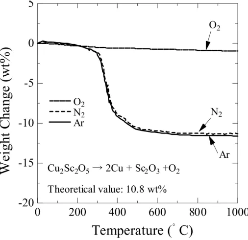
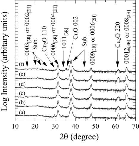
The thermogravimetric analysis (TGA) was carried out to study the thermal characteristics of bulk Cu2Sc2O5. Figure 2-5 shows the TGA profiles of bulk Cu2Sc2O5
under different gas atmospheres. No weight change of the bulk was observed in oxygen; however, significant weight changes were detected in reducing gases such as argon and nitrogen above approximately 300°C. This large weight loss agreed closely with the theoretical value expected for the decomposition reaction that forms Cu and Sc2O3 from
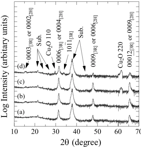
Cu2Sc2O5. XRD 2θ-ω patterns of the reaction samples are shown in Fig. 2-6. Several Cu
and Sc2O3 peaks were detected only for the sample heated in nitrogen gas, indicating
that Cu2Sc2O5 decomposes into Cu and Sc2O3. It has been well documented that copper
metal oxidized into Cu2O and CuO in that order under increasing oxygen pressure [5].
Consequently, we concluded that it was possible to prepare a CuScO2 thin film by using
a single-phase Cu2Sc2O5 target while controlling oxygen pressure and substrate
temperature.
2.3.2 Substrate temperature dependence of film quality
Figure 2-7 shows the XRD 2θ-ω patterns of CuScO2 thin films prepared at
various substrate temperatures. Other deposition parameters are as follows: an oxygen pressure of 0.5 Pa, an rf forward power of the oxygen radical source of 0 W, a laser fluence of 2.6 Jcm-2, a laser repetition frequency of 1 Hz, and a deposition time of 1 h.
0
200
400
600
800
1000
-20
-15
-10
-5
0
5
Temperature (゚C)
Weig
ht
C
han
ge
(
w
t%
)
O
2N
2Ar
Cu
2Sc
2O
5→ 2Cu + Sc
2O
3+O
2Theoretical value: 10.8 wt%
O
2N
2Ar
Fig. 2-5 TGA profiles of bulk Cu2Sc2O5 samples under different gas atmospheres.
10
20
30
40
50
60
2θ (degree)
In
ten
sity
(
ar
bitar
y u
nits
)
O
2gas
N
2gas
○
○
○
○
○
●
Cu
○
Sc
2O
3●
●
Fig. 2-6 XRD 2θ-ω patterns of reaction samples after TGA measurements in nitrogen and oxygen atmospheres. Several peaks for Cu (●) and Sc2O3 (○) were
Only diffraction peaks corresponding to CuScO2 000l were observed at substrate
temperatures of 800 °C and 850 °C, where the l values corresponded to 3,6,9,12 if the structure of the film supposed to be 3R and to 2,4,6,8 if it supposed to be 2H. The intensities for their diffraction peaks increased with increasing substrate temperature, but became weaker at a substrate temperature of 950 °C. Additional diffraction peaks corresponding to Cu2O 110, 220 and CuScO2[3R] 1011 also appeared when the
substrate temperature exceeded 850 °C.
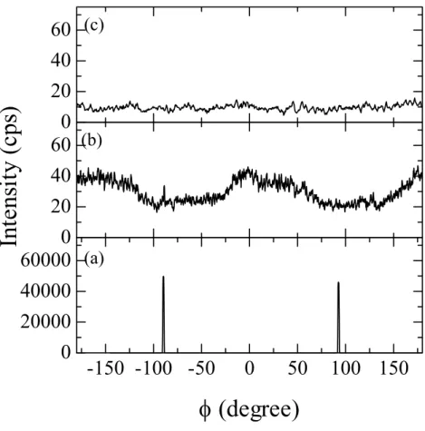
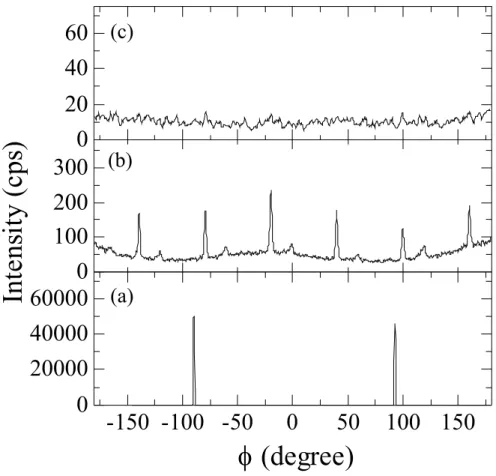
The in-plane orientation relationship of the film with respect to the substrate for the film deposited at a substrate temperature of 850 °C was investigated using XRD φ-scan measurements. The results using 3030 diffractions of the substrate, 1014
diffractions of the CuScO2[3R] phase, and 1013 diffractions of the CuScO2[2H] phase
of the film are shown in Fig. 2-8. Peaks with two-fold rotational symmetry were observed for 3030 diffractions of the substrate. On the other hand, no peaks for the
4 1
10 diffractions of the CuScO2[3R] phase and 1013 diffractions of the CuScO2[2H]
phase of the film were observed, indicating that the film has no in-plane orientations. The substrate temperature dependence of the deposition rate and the concentration ratio of Cu/(Cu+Sc) in deposited films are shown in Fig. 2-9. All concentration ratios of Cu/(Cu+Sc) were normalized by that of the film deposited at a substrate temperature of 900 °C. The deposition rate increased when the substrate temperature exceeded 850 °C. On the other hand, the concentration of Cu was almost constant within a substrate temperatures ranging from 800 °C to 900 °C, and slightly decreased at a substrate temperature of 950 °C.
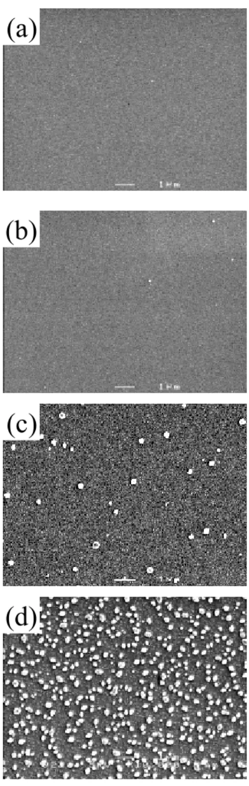
The surface morphologies of the deposited films were examined using SEM observation. The images are illustrated in Fig. 2-10. There were few precipitates on the
10
20
30
40
50
60
70
2θ (degree)
Lo
g I
nten
sity
(
ar
bitar
y u
nits
)
(b)
0006
[3 R ]or 0004
[2 H]0009
[3 R ]or 0006
[2 H ]00012
[3 R ]or 0009
[2 H]Cu
2O 220
Su
b.
(c)
(d)
Su
b.
(a)
Cu
2O 110
1011
[3 R ]0003
[3 R ]or 0002
[2 H]Fig. 2-7 XRD 2θ-ω patterns of CuScO2 thin films deposited on a-plane sapphire
substrates at various substrate temperatures. (a) 800 °C, (b) 850 °C , (c) 900 °C, and (d) 950 °C.
-150 -100 -50
0
50
100 150
0
20000
40000
60000
φ (degree)
In
ten
sity
(
cp
s)
(a)
(b)
(c)
0
20
40
60
0
20
40
60
Fig. 2-8 XRD φ-scans of a-plane sapphire substrate and CuScO2(0001) thin film
deposited at a substrate temperature of 850 °C. (a)
{ }
3030 plane of substrate, (b){ }
1014 plane of CuScO2[3R] phase of film, (c){ }
1013 plane of800
850
900
950
0
1.0
2.0
3.0
0.4
0.6
0.8
1.0
1.2
Substrate Temperature (℃)
D
ep
os
itio
n R
ate (
nm min
-1)
Cu/
(Cu+
Sc
)
Deposition Rate
Cu/(Cu+Sc)
Fig. 2-9 Substrate temperature dependences of deposition rate and concentration ratio of Cu/(Cu+Sc) on CuScO2 thin films. All concentration ratios of Cu/(Cu+Sc)
were normalized by that of the film deposited at a substrate temperature of 900 °C.
(a)
(c)
(b)
1μm(d)
(a)
(a)
(c)
(b)
(b)
1μm(d)
1μm 1μm(d)
Fig. 2-10 SEM images of CuScO2 thin films prepared on a-plane sapphire substrates
under substrate temperatures of (a) 800 °C, (b) 850 °C, (c) 900 °C, and (d) 950 °C.
film surface when the film was prepared below a substrate temperature of 850 °C, as shown in Fig. 2-10(a) and 2-10(b). A small amount of precipitates was observed on the film surface prepared at a substrate temperature of 900 °C [Fig. 2-10(c)], and a substrate temperature of 950 °C caused a large number of precipitates with a size of about 50-200 nm to form on the whole surface, as shown in Fig. 2-10(d).
Consequently, the increase in the deposition rate is because the film surface becomes rougher due to a large number of precipitations generated by the thermal decomposition reaction in deposited films.
2.3.3 Oxygen pressure dependence of film quality
Figure 2-11 shows the XRD 2θ-ω patterns of CuScO2 thin films deposited under
various oxygen pressures. Other deposition parameters are as follows: a substrate temperature of 900 °C, an rf forward power of the oxygen radical source of 0 W, a laser fluence of 2.6 Jcm-2, a laser repetition frequency of 1 Hz, and a deposition time of 1 h. Diffraction peaks corresponding to CuScO2 000l and 1011, Cu2O 110 and 220 were
observed at an oxygen pressure of 1.0×10⁻¹ Pa. With increasing oxygen pressure, the
intensities for the diffraction peaks corresponding to CuScO2 000l increased and
those for the diffraction peaks corresponding to CuScO2 1011, Cu2O 110, 220 peaks
became smaller. Only diffraction peaks corresponding to CuScO2 000l was identified
at an oxygen pressure of 1.5 Pa, indicating that a strongly c-axis oriented CuScO2 thin
film can be grown on an a-plane sapphire substrate. The intensities from CuScO2 000l
diffraction peaks decreased, and Cu2O 110, 220 and CuO 002 peaks appeared when the
oxygen pressure exceeded 1.5 Pa.
The XRD φ-scans using 3030 diffractions of the substrate, 1014 diffractions of the CuScO2[3R] phase and 1013 diffractions of the CuScO2[2H] phase of the film
10
20
30
40
50
60
70
2θ (degree)
L
og Int
ens
it
y (a
rbi
ta
ry uni
ts
)
(a)0006
[3 R ]or 0004
[2 H ]0009
[3 R ]or 0006
[2 H]00012
[3 R ]or 0008
[2 H ]Sub.
Cu
2O 110
Cu
2O 220
CuO 002
(b) (c) (d) (e) (f)Sub.
1011
[3 R ]0003
[3 R ]or 0002
[2 H ]Fig. 2-11 XRD 2θ-ω patterns of CuScO2 thin films deposited on a-plane sapphire
substrates at various oxygen pressures. (a) 1.0×10⁻¹ Pa, (b) 5.0×10⁻¹ Pa, (c)
0
20
40
60
-150 -100 -50
0
50 100 150
0
20000
40000
60000
φ (degree)
Int
en
si
ty
(c
ps
)
(a)
(b)
(c)
0
100
200
300
Fig. 2-12 XRD φ-scans of a-plane sapphire substrate and CuScO2(0001) thin film
prepared at an oxygen pressure of 1.5 Pa. (a)
{ }
3030 plane of substrate, (b){ }
1014 plane of CuScO2[3R] phase of film, (c){ }
1013 plane ofprepared at an oxygen pressure of 1.5 Pa are shown in Fig. 2-12. For the 1014
diffractions of the CuScO2[3R] phase of the film, the mixture of two types of six-fold
rotational symmetry components were observed, as shown in Fig. 2-12(b). On the other hand, no peaks for the 1013 diffractions of the CuScO2[2H] phase of the film were
detected.
The deposition rate and the concentration ratio of Cu/(Cu+Sc) in deposited films are shown in Fig. 2-13 as a function of the oxygen pressure. All concentration ratios of Cu/(Cu+Sc) were normalized by that of the film deposited at an oxygen pressure of 1.5 Pa. The deposition rate decreased and the concentration of Cu showed no distinct dependence on oxygen pressures ranging from 1.0×10⁻¹ Pa to 1.5 Pa. In the case of
relatively low oxygen pressures and/or high substrate temperatures during the deposition, we consider that the thermal decomposition reaction (2CuScO2 → Cu2O +
Sc2O3) does proceed in deposited films. This reaction generates grains with different
orientations and phases, as shown in Fig. 2-11. The grains may have different growth speeds, causing the film surface to become rough. However, the average composition of the film must be kept constant. Consequently, a decrease in the deposition rate occurs because the thermal decomposition reaction in deposited films is suppressed by increasing oxygen pressure. With further increases in oxygen pressure, both the deposition rate and the concentration of Cu increased. It is well known that excess elements in deposited films are separated as impurity phases on the film surface at higher deposition temperatures [6].
The SEM observation was carried out to examine the surface morphologies of the deposited films. The images are illustrated in Fig. 2-14. With increasing oxygen pressure, the precipitates on the film surface decreased, and there were few precipitates on the film surface when the film was prepared at an oxygen pressure of 1.5 Pa, as
10
-110
010
10
1.0
2.0
3.0
0.2
0.4
0.6
0.8
1.0
1.2
Oxygen Pressure (Pa)
D
epos
it
io
n Ra
te
(nm
m
in
-1)
Cu/
(Cu+
Sc
)
Deposition Rate
Cu/(Cu+Sc)
Fig. 2-13 Deposition rate and concentration ratio of Cu/(Cu+Sc) on CuScO2 thin
films as a function of the oxygen pressure. All concentration ratios of Cu/(Cu+Sc) were normalized by that of the film deposited at an oxygen pressure of 1.5 Pa.
(a)
(d)
1μm(f)
(c)
(e)
(b)
(a)
(a)
(d)
1μm(f)
1μm 1μm(f)
(c)
(e)
(e)
(b)
Fig. 2-14 SEM images of CuScO2 thin films prepared on a-plane sapphire substrates
under oxygen pressures of (a) 1.0×10⁻¹ Pa, (b) 5.0×10⁻¹ Pa, (c) 1.0 Pa, (d)
shown in Fig. 2-14(d). With further increases in oxygen pressure, the precipitates on the film surface increased, and an oxygen pressure of 5.0 Pa caused a large number of precipitates with a size of about 50-300 nm to form on the whole surface, as shown in Fig. 2-14(f). In summary, the increase in the deposition rate at an oxygen pressures above 1.5 Pa is caused by the generation of the precipitates on the film surface due to deviations in the stoichiometry of the film’s composition.
2.3.4 Fabrication of CuScO
2(0001) epitaxial films and the effect of laser
fluence on the in-plane orientation of the epitaxial films
To obtain CuScO2(0001) epitaxial films, CuScO2 thin films were prepared at a
substrate temperature of 925 °C using the oxygen radical source to suppress the thermal decomposition reaction during deposition. The XRD 2θ-ω and RHEED patterns of the CuScO2 thin film, deposited at a substrate temperature of 925 °C, an oxygen pressure of
1.5 Pa, an rf forward power of the oxygen radical source of 200 W, a laser fluence of 2.6 Jcm-2, a laser repetition frequency of 1 Hz, and a deposition time of 2 h, are shown in Figs. 2-15 and 2-16, respectively. Only CuScO2 000l diffraction peaks were observed,
indicating that the film is strongly oriented with the c-axis perpendicular to the substrate. Streaky RHEED patterns showing six-fold rotational symmetry were observed. However, identifying the crystallographic structure of the c-axis oriented film using conventional XRD 2θ-ω measurements was difficult because the diffraction angles of
l
000 peaks for each phase were very close. Therefore, two-dimensional X-ray reciprocal space mapping measurements were conducted, as shown in Fig. 2-17. Diffractions corresponding to 000l0
[
l0 =6,9,12]
, 101l1[
l1 =1,2,4,8,10]
, and[
2]
2
20 l2 l2 = of CuScO2 with 3R crystal structure were observed, suggesting that
10
20
30
40
50
60
70
10
010
110
210
310
410
510
610
710
82θ (degree)
In
ten
sity
(
cp
s)
0006 [3 R ] or 0004 [2 H ] 0009 [3 R ] or 0006 [2 H ] 00012 [3 R ] or 0008 [2H ] S ub. 0003 [3 R ] or 0002 [2 H ]Fig. 2-15 XRD 2θ-ω pattern of a CuScO2 thin film grown on an a-plane sapphire
substrate. The film was deposited at a substrate temperature of 925°C, an oxygen pressure of 1.5 Pa, an rf forward power of 200 W, a laser fluence of 2.6 Jcm-2, a laser repetition frequency of 1 Hz, and a deposition time of 2 h.
[ ]
10
1
0
[ ]
11
2
0
[ ]
10
1
0
[ ]
10
1
0
[ ]
11
2
0
[ ]
11
2
0
Fig. 2-16 RHEED patterns of a CuScO2 thin film deposited on an a-plane sapphire
substrate. The electron beam was incidental along
[ ]
1010 and[ ]
1120 azimuths.(
20 l
2
2
)
3
R
[
l
2=
2
]
( )
10 l
1
1
3
R
[
l
1=
1
,
2
,
4
,
8
,
10
]
(
000l
0)
3R[
l
0
=
6
,
9
,
12
]
( )
22
4
0
S
( )
11
2
0
S
(
20 l
2
2
)
3
R
[
l
2=
2
]
( )
10 l
1
1
3
R
[
l
1=
1
,
2
,
4
,
8
,
10
]
(
000l
0)
3R[
l
0
=
6
,
9
,
12
]
( )
22
4
0
S
( )
11
2
0
S
(
20 l
2
2
)
3
R
[
l
2=
2
]
( )
10 l
1
1
3
R
[
l
1=
1
,
2
,
4
,
8
,
10
]
(
000l
0)
3R[
l
0
=
6
,
9
,
12
]
( )
22
4
0
S
( )
11
2
0
S
(
20 l
2
2
)
3
R
[
l
2=
2
]
( )
10 l
1
1
3
R
[
l
1=
1
,
2
,
4
,
8
,
10
]
(
000l
0)
3R[
l
0
=
6
,
9
,
12
]
( )
22
4
0
S
( )
11
2
0
S
Fig. 2-17 Two-dimensional X-ray reciprocal space mapping measurements of the c-axis oriented CuScO2 thin film grown on an a-plane sapphire substrate.
Diffractions corresponding to 000l0
[
l0 =6,9,12]
, 101l1[
l1 =1,2,4,8,10]
, and 202l2[
l2 =2]
of CuScO2 with 3R crystal structure were observed.0
200
400
600
800
1000
-150 -100 -50
0
50 100 150
0
20000
40000
60000
In
ten
sity
(
cp
s)
φ (degree)
(b)
(a)
9°
0
200
400
600
800
1000
-150 -100 -50
0
50 100 150
0
20000
40000
60000
In
ten
sity
(
cp
s)
φ (degree)
(b)
(a)
9°
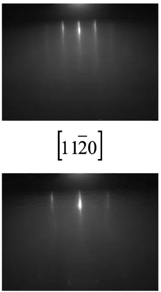
Fig. 2-18 XRD φ-scans of a-plane sapphire substrate and CuScO2[3R](0001) thin
film.
maximum (FWHM) value taken from a 0006-peak rocking curve measurement was 0.14°.
The XRD φ-scans using 3030 diffractions of the substrate and 1014
diffractions of the film are shown in Figs. 2-18(a) and 2-18(b), respectively. Sharp peaks with two-fold rotational symmetry were observed for 3030 diffractions of the substrate. On the other hand, peaks for the 1014 diffractions of the film exhibited six-fold rotational symmetry, indicating that the film had twin structures. However, the peaks of the film did not show agreement with those of the substrate at the φ diffraction angles of ±90°, and shifted from those of the substrate about 9°. Since it is possible that Cu+ layers or (ScO2)- octahedral layers form the CuScO2[3R](0001) plane, this may be
due to the atomic arrangements of the initial growth of CuScO2[3R](0001) epitaxial
films on a-plane sapphire substrates. Therefore, the effect of the laser fluence on the film quality of CuScO2 thin films was investigated, because the in-plane orientation of
ZnO thin films grown on c-plane sapphire substrates has been reported to be controlled by the laser fluence [7]. Other deposition parameters are set as follows: a substrate temperature of 925 °C, an oxygen pressure of 1.5 Pa, an rf power of the oxygen radical source of 200 W, a laser repetition frequency of 1 Hz, and a deposition time of 1–2 h. Figure 2-19 shows the XRD 2θ-ω patterns of CuScO2 thin films deposited at
various laser fluences. Only diffraction peaks corresponding to CuScO2 000l were
identified for the film prepared at a laser fluence of 0.6 Jcm-2. With increasing laser fluence, the intensities for CuScO2 000l diffraction peaks became stronger and
additional diffraction peaks corresponding to Cu2O 110, 111, 200, and 220 appeared.
However, the intensities for Cu2O diffraction peaks became smaller when the laser
fluence exceeded 1.0 Jcm-2, and only CuScO2 000l peaks were observed for the film
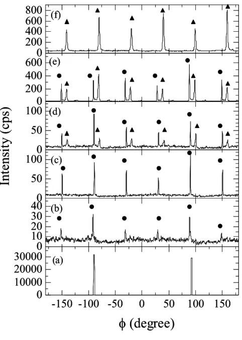
The in-plane orientation of the films, shown in Fig. 2-19, against the substrates was characterized using XRD φ-scan measurements. The results obtained using 3030 diffractions of the substrate, 1014 diffractions of the CuScO2[3R] phase and 1013
diffractions of the CuScO2[2H] phase of the films are shown in Figs. 2-20 and 2-21.
Peaks with two-fold rotational symmetry were observed for 3030 diffractions of the substrate, as shown in Figs. 2-20(a) and 2-21(a). However, peaks for 1014 diffractions of the films prepared at a laser fluence of less than or equal to 1.0 Jcm-2 exhibited six-fold rotational symmetry and were in agreement with 3030 diffractions of the substrate at φ diffraction angles of ±90° [Figs. 2-20(b) and 2-20(c)]. This indicates that the domain with CuScO2
[ ]
3R[ ]
1120 //sapphire[
0001]
in-plane orientation grows on a-plane sapphire substrates. With increasing laser fluence, new peaks corresponding to another six-fold rotational symmetry component appeared, as shown in Figs. 2-20(d) and 2-20(e), and their intensities became stronger. This indicates that the films have two types of domain in the basal plane. Only new peaks corresponding to another six-fold rotational symmetry component were observed for the film prepared at a laser fluence of 2.6 Jcm-2 [Fig. 2-20(f)]. On the other hand, no peaks for the 1013 diffractions of the CuScO2[2H] phase of the films were observed, as shown in Fig. 2-21.The deposition rate and the concentration ratio of Cu/(Cu+Sc) in deposited films are shown in Fig. 2-22 as a function of the laser fluence. All concentration ratios of Cu/(Cu+Sc) were normalized by that of the film deposited at a laser fluence of 2.6 Jcm-2. The deposition rate increased with increasing laser fluence and decreased slightly when the laser fluence was 1.1 Jcm-2. With further increases in laser fluence, the deposition rate increased again. On the other hand, the concentration of Cu in the film prepared at a laser fluence of 0.6 Jcm-2 was almost identical to that in the film prepared at a laser fluence of 2.6 Jcm-2. The concentration of Cu increased with increasing laser fluence,
10
20
30
40
50
60
70
2θ (degree)
Lo
g I
nten
sity
(
ar
bitar
y u
nits
)
(a)
0006
[3 R ]0009
[3 R ]00012
[3 R ]Sub.
Cu
2O 110
Cu
2O 220
(b)
(c)
(d)
Cu
2O 200
Cu
2O 11
1
0003
[3 R ](e)
(f)
Fig. 2-19 XRD 2θ-ω patterns of CuScO2 thin films deposited on a-plane sapphire
substrates at various laser fluences. (a) substrate, (b) 0.6 Jcm-2 (c) 1.0 Jcm-2, (d) 1.1 Jcm-2, (e) 1.8 Jcm-2, and (f) 2.6 Jcm-2. Other deposition parameters are as follows: a substrate temperature of 925 °C, an oxygen pressure of 1.5 Pa, an rf forward power of the oxygen radical source of 200 W, a laser repetition frequency of 1 Hz, and a deposition time of 1∼2 h.
0
200
400
600
800
-150 -100 -50
0
50 100 150
0
10000
20000
30000
φ (degree)
In
ten
sity
(
cp
s)
(a)
(b)
(c)
(d)
(e)
(f)
0
50
100
0
50
100
0
200
400
600
0
10
20
30
40
0
200
400
600
800
-150 -100 -50
0
50 100 150
0
10000
20000
30000
φ (degree)
In
ten
sity
(
cp
s)
(a)
(b)
(c)
(d)
(e)
(f)
0
50
100
0
50
100
0
200
400
600
0
10
20
30
40
Fig. 2-20 XRD φ-scans of
{ }
3030 plane of sapphire substrate and{ }
1014 plane of CuScO2[3R] phase of the films deposited at various laser fluences. (a)substrate, (b) 0.6 Jcm-2 (c) 1.0 Jcm-2, (d) 1.1 Jcm-2, (e) 1.8 Jcm-2, and (f) 2.6 Jcm-2. Two kinds of six-fold rotational symmetry components were observed, and each component indicates using next symbols [(●) and (▲)].
0
10
20
-150 -100 -50
0
50 100 150
0
2000
4000
6000
φ (degree)
In
ten
sity
(
cp
s)
(a)
(b)
(c)
(d)
(e)
(f)
0
10
20
0
10
20
0
10
20
0
10
20
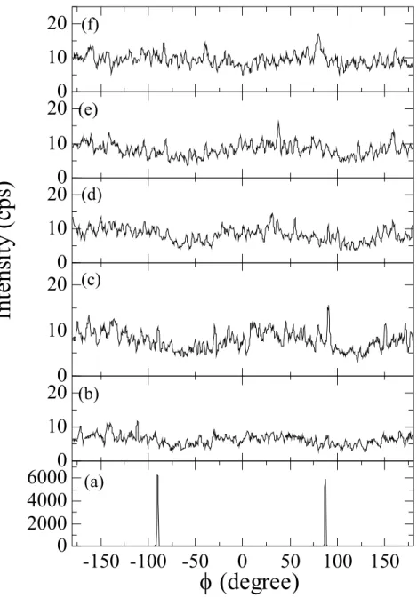
Fig. 2-21 XRD φ-scans of
{ }
3030 plane of sapphire substrate and{ }
1013 plane of CuScO2[2H] phase of the films deposited at various laser fluences. (a)substrate, (b) 0.6 Jcm-2 (c) 1.0 Jcm-2, (d) 1.1 Jcm-2, (e) 1.8 Jcm-2, and (f) 2.6 Jcm-2. No peaks for the 1013 diffractions of the CuScO2[2H] phase of the
1
2
3
0.2
0.4
0.6
0.8
0.2
0.4
0.6
0.8
1.0
1.2
1.4
1.6
0
Laser Fluence (Jcm
-2)
D
epos
it
io
n Ra
te
(nm
m
in
-1)
Cu/
(Cu+
Sc
)
Deposition Rate
Cu/(Cu+Sc)
Fig. 2-22 Deposition rate and concentration ratio of Cu/(Cu+Sc) on CuScO2 thin
films as a function of the laser fluence. All concentration ratios of Cu/(Cu+Sc) were normalized by that of the film deposited at a laser fluence of 2.6 Jcm-2.
but gradually decreased when the laser fluence exceeded 1.0 Jcm-2. Consequently, the increase in the deposition rate at a laser fluence of 1.0 Jcm-2 is because the film surface becomes rougher due to the precipitates generated by the compositional deviation in the film.
Optical emission spectra were measured to study the laser fluence dependence of the excited species in the plume. For example, Figure 2-23 shows the optical emission spectrum of the plume when the target was ablated at a laser fluence of 2.6 Jcm-2. Emission lines including radicals, and singly and molecular ionized species for each element were identified in accordance with standard tables of spectral lines [2.3]. Molecular band heads in relation to ScO were also detected. Therefore, the typical peaks for each excited species were chosen, and their emission intensities were measured as a function of the laser fluence. These peaks are a copper ion (Cu+; 214nm), a copper radical (Cu*; 325nm), a scandium ion (Sc+; 361nm), a scandium radical (Sc*; 391nm), a molecular oxygen ion (O2+; 642nm), an oxygen radical (O*; 777nm), and a
molecular scandium oxide (ScO; 604nm), respectively. The results are shown in Fig. 2-24. The emission intensities for Sc*, O*, and ScO were almost zero at a laser fluence ranging from 0.6 to 1.0 Jcm-2, and those for another excited species showed no distinct dependence. The emission intensity for ScO began to increase when the laser fluence exceeded 1.0 Jcm-2. With further increasing laser fluences, the emission intensities for Cu* and Sc*, Sc+ and ScO abruptly increased. On the other hand, the emission intensity for Cu+ was almost constant, and those for O2+ and O* gradually increased. By
comparing these results to those shown in Fig. 2-20, we notice that another six-fold rotational symmetry component (▲ in the figure) appears when the emission intensities for Cu* and Sc*, Sc+ and ScO begin to increase, and that preferentially grows as their emission intensity increase.
200
400
600
800
1000
2000
3000
Wavelength (nm)
Int
ens
it
y (a
rbi
ta
ry uni
ts
)
KrF
Cu*
ScO
Sc*
Sc*,
Cu
+,
O
2+}
Fig. 2-23 Optical emission spectrum of the plume from the target ablated at a laser fluence of 2.6 Jcm-2. Emission lines including radicals, and singly and molecular ionized species for each element were identified and molecular band heads in relation to ScO were also detected.
0 1000 2000 Cu+ (214nm) Cu* (325nm) In te ns itie s o f Cu + and C u* (a rb ita ry u nits ) 0 1000 2000 3000 In te ns itie s o f Sc + a nd Sc* (a rb ita ry u nits ) Sc+ (361nm) Sc* (391nm) 0 100 200 300 In te ns itie s o f O2 + a nd O * (a rb it ary u ni ts ) O2+ (642nm) O* (777nm) 0 1 2 3 0 200 400 600 In te ns ity o f S cO (a rb ita ry u nits )
Laser fluence (Jcm
-2)
ScO (604nm)Fig. 2-24 Intensities of typical peaks for each excited species as a function of the laser fluence. The peaks are Cu+(214nm), Cu*(325nm), Sc+(361nm), Sc*(391nm), O2+(642nm), O*(777nm), and ScO(604nm), respectively.
Here, we consider the atomic arrangements for the CuScO2[3R](0001) and
sapphire
( )
1120 planes. The CuScO2[3R] one is composed of an alternating stack ofCu+ layers and (ScO2)- octahedral layers along the c-axis [Fig. 1-1(b)], thus it is possible
that Cu+ layers or (ScO2)- octahedral layers form the CuScO2[3R](0001) plane. On the
other hand, both Al and O atoms exist in the sapphire
( )
1120 plane, as shown in Fig. 2-25. If Cu+ layers form the CuScO2[3R](0001) plane, the Cu atoms of the layers formbonds with O atoms on the sapphire surface. The in-plane orientation relationship between the substrate and the film, shown in Fig. 2-26(a), is
[ ]
3R[ ]
1120 //sapphire[
0001]
CuScO2 and the distance between two neighboring O
atoms along with sapphire
[
0001]
direction (c-axis lattice constant of sapphire) matches the four-fold longer constants of CuScO2[3R][ ]
1120 with less than a 0.98%misfit. On the contrary, if (ScO2)- octahedral layers form the CuScO2[3R](0001) plane,
the O atoms of the layers form bonds with Al atoms on the sapphire surface. In this case, the distance between two neighboring Al atoms along with sapphire
[ ]
2201 direction matches the three-fold longer constants of CuScO2[3R][ ]
1120 with less than a 0.98%misfit when the in-plane orientation relationship between the substrate and the film is
[ ]
3R[ ]
1120 //sapphire[ ]
2201CuScO2 [Fig. 2-26(b)]. The angle between sapphire
[ ]
2201 and[ ]
1100 directions is 38.24°, as shown in Fig. 2-25. Therefore, the angle between CuScO2[3R][ ]
1120 and sapphire[ ]
1100 directions is 8.24 °. This agrees wellwith the result shown in Fig. 2-18.
Consequently, it is presumed that two kinds of in-plane orientation for the epitaxial growth of CuScO2[3R](0001) thin films on a-plane sapphire substrates are
influenced by the atomic arrangements (Cu+ layers or (ScO2)- octahedral layers) of the
1.2991 nm 0.8241 nm 38.24° 38.24° ① ② ③ ④ ⑤ ⑥ 9.93° 30.00° 0.8769 ⑥ 0.7470 ⑤ 0.9743 ④ 0.7470 ③ 1.1042 ② 0.9743 ① Length (nm) 0.8769 ⑥ 0.7470 ⑤ 0.9743 ④ 0.7470 ③ 1.1042 ② 0.9743 ① Length (nm)
Fig. 2-25 Schematic representation of sapphire
( )
1120 plane. Large and small dark circles represent O and Al atoms, respectively [8]. Table summarizes the length between neighboring Al atoms in a distorted hexagonal lattice.
Sapphire
CuScO
2[3R]
Cu atom O atomSapphire
CuScO
2[3R]
Al atom(a) Cu
+layers
(b) (ScO
2)
-layers
O atomCuScO
2[3R](0001) plane
( : Cu atom)
Sapphire
CuScO
2[3R]
Cu atom O atomSapphire
CuScO
2[3R]
Al atom(a) Cu
+layers
(b) (ScO
2)
-layers
O atomCuScO
2[3R](0001) plane
( : Cu atom)
Fig. 2-26 Schematic diagram of a lattice for CuScO2[3R](0001) and sapphire
( )
1120planes. CuScO2[3R](0001) epitaxial films with two kinds of in-plane
orientation are possible to be grown on a-plane sapphire substrates by the atomic arrangements of the initial growth of the films, and their in-plane orientation relationships are as follows :
(a) CuScO2
 thin film](https://thumb-ap.123doks.com/thumbv2/123deta/8512210.1805564/45.892.187.697.362.854/fig-xrd-scans-plane-sapphire-substrate-cusco-film.webp)