Hot and Ultrafast Carrier Extraction from
Colloidal Semiconductor Nanocrystals with
Different Quantum Confinement Dimensionality
著者(英)
Tomoki Okuhata
学位名
博士 (理学)
学位授与機関
関西学院大学
学位授与番号
34504甲第624号
Hot and Ultrafast Carrier Extraction from
Colloidal Semiconductor Nanocrystals with
Different Quantum Confinement Dimensionality
Thesis for the Degree of
Doctor of Science
Submitted to
School of Science and Technology
Kwansei Gakuin University
Tomoki OKUHATA
Chapter 1
Introduction
1.1 Preface
1.2 Semiconductor nanocrystals
1.2.1 General properties of semiconductor quantum dots 1.2.2 Shape control of semiconductor nanocrystals 1.2.3 Electronic structures of semiconductor nanocrystals
1.2.4 Exiton dynamics of semiconductor nanocrystals 1.3 Carrier transfer from semiconductor nanocrystals 1.3.1 Electron transfer in molecular chromophores 1.3.2 Electron transfer in semiconductor nanocrystals 1.4 Outline of this thesis
Chapter 2
Synthesis of Colloidal Semiconductor Nanocrystals and
Semiconductor-metal HNs
2.1 CdSe/CdS core/shell QD and core/shell QD-MV2+ complexes
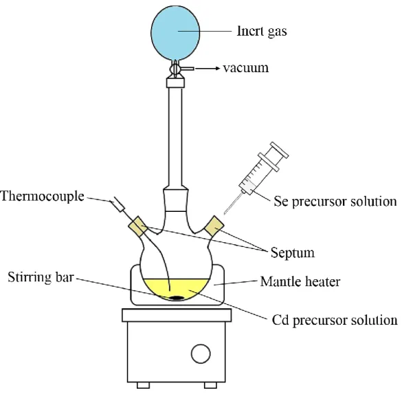
a) Synthesis of CdSe/CdS core/shell QDs
b) Preparation of CdSe/CdS core/shell QD-MV2+ complexes
2.2 4-monolayer CdSe NPLs and CdSe NPL-MV2+ complexes a) Synthesis of CdSe NPLs with different lateral size b) Preparation of CdSe NPL-MV2+ complexes 2.3 Oleylamine capped PbS QDs and PbS QD-Au HNs a) Synthesis of PbS QDs
2.4 Au NPs attached CdSe nanocrystals with different quantum confinement dimensionality a) Synthesis of CdSe QDs
b) Synthesis of CdSe NPLs
c) Synthesis of CdSe QD-Au HNs and NPL-Au HNs
Chapter 3
Hot Electron Transfer from CdSe/CdS Core/shell QD to Methyl Viologen
3.1 Abstract 3.2 Introduction
3.3 Experimental section 3.4 Results and discussion 3.5 Conclusion
Chapter 4
Elementary Electron Transfer Processes from CdSe NPL to Methyl
Viologen
4.1 Abstract 4.2 Introduction
4.3 Experimental section 4.4 Results and discussion
4.4.1 Elementary electron transfer processes from CdSe NPL to MV2+ 4.4.2 The assignment of transient absorption bands of CdSe NPLs 4.5 Conclusion
Chapter 5
Ultrafast and Hot Carrier Dynamics in PbS QD-Au HNs
5.1 Abstract 5.2 Introduction
5.3 Experimental section 5.4 Results and discussion 5.5 Conclusion
Chapter 6
Ultrafast and Hot Electron Transfer Processes from CdSe QD to Au NPs
6.1 Abstract 6.2 Introduction
6.3 Experimental section 6.4 Results and discussion
6.4.1 Electron transfer processes from CdSe QDs to Au NPs 6.4.2 Electron transfer processes from CdSe NRs to Au NPs 6.5 Conclusion
Chapter 7
Electron Transfer Processes from CdSe NPL to Au NPs
7.1 Abstract 7.2 Introduction
7.4 Results and discussion 7.5 Conclusion
Summary
Acknowledgement
1
Chapter 1
Introduction
2
1.1 Preface
In the semiconductor nanocrystals, electron and hole are confined in the region smaller than the exciton Bohr radius. The strong confinement of electron and hole leads to the various unique properties in semiconductor nanocrystals, for example, size-tunable optical absorption and emission spectra, discrete energy states, strong electron-hole interaction etc. In 1982, the first synthesis of colloidal CdS nanocrystals in the reversed micelle was reported by Henglein group1 and Brus group.2 Then, the size dependent electronic spectra where the band-edge absorption shifted to the longer wavelength region as the size of nanocrystals increase were clearly observed, and this phenomenon is well known as the quantum size effect.3 The further progress in the colloidal synthesis of semiconductor nanocrystals was achieved by Murray et al. in 1993.4 They reported the synthetic method of high quality CdSe,
CdS, and CdTe quantum dots (QDs) using organometallic compounds (dimethylcadmium and Se-trioctylphosphine) at high temperature. Furthermore, the synthesis of several kinds of core/shell QDs in which the surface of core QDs was coated with the different semiconductor shell were reported.5,6 These core/shell nanocrystals can be classify into type I, quasi-type II,
and type II by the difference of the energy of conduction and valence band-edge states. In the type I core/shell nanocrystals, the energy levels of conduction and valence band-edge states of shell were higher than those of core nanocrystals, indicating electron and hole wavefunctions were confined core region. Moreover, by passivating surface defects with the shell, the remarkable increase of luminescence quantum yield was observed in type I core/shell nanocrystals.5,6 In the quasi-type II core/shell nanocrystals, only the electron (hole)
wavefunction spread over the whole core/shell nanocrystals, and hole (electron) wavefuncton was confined in the core region.7,8 In the type II core/shell nanocrystals, electron and hole
wavefunctions were separated in the core and shell region. Consequently, the overlap of electron and hole wavefunctions reduces in the type II core/shell nanocrystals, leading that the
3
radiative lifetime becomes longer.9,10 In 2000, Peng et al. reported the one-dimensional growth of wurtzite CdSe nanocrystals where electron and hole were confined in the short axis direction.11 The important factors in the shape control of nanocrystals are the crystal structure, precursor concentration, and capping reagents.11-15 In addition to QDs (three dimensional confinement) and NRs (two dimensional confinement), S. Ithurria and B. Dubertret synthesized colloidal semiconductor nanoplatelets (NPLs, one dimensional confinement) with atomic-layer precision in 2008.16 The two dimensional growth of NPLs was achieved by the selective passivation of the (100) face of zinc-blend CdSe nanocrystals with carboxylic acid.17-19 Colloidal semiconductor NPLs exhibit thickness-tunable, bright luminescence with narrow line width, and large absorption cross section.20-22 Then, synthetic methods of
core/shell and core/crown heterostructure-NPLs were reported.19,23,24 The control of quantum confinement dimensionality leads to the variation of electronic structures and carrier relaxation processes. Furthermore, Mokari et al. have reported the synthesis and characterization of semiconductor-metal hybrid nanostructures (HNs) where metal nanoparticles (NPs) attached semiconductor NRs, tetrapods, and QDs.25,26 Much attention has been paid for these HNs in terms of photovoltaics and photocatalysis because of the efficient charge separation between semiconductor and metal.
Since the semiconductor nanocrystals have discrete energy states, photoexcited hot carriers relax to the band-edge state through different processes from bulk semiconductor. For bulk semiconductor, hot carrier relax to the band-edge state immediately via phonon emission. However, in the semiconductor QDs where the energy separation between 1S and 1P states is much larger than the phonon energy,27 the hot carrier relax via energy transfer between
electron and hole,28-32 energy transfer to the vibrational state of capping reagents,33 and multiphonon emission.34 The rate constant of these mechanisms can be controlled by capping
4
Actually, Pandey and Gyot-Sionnest reported the extremely slow hot electron relaxation with the lifetime over 1 ns in CdSe/ZnSe/ZnS/CdSe multishell QDs.35 Consequently, the slow intraband reraxation in semiconductor nanocrystals can potentially allow for efficient hot carrier extraction. Furthermore, the enhancement of electron-hole interaction in semiconductor nanocrystals leads to the highly efficient multiple exciton generation (MEG) in which multiexcitons generate from the absorption of only one photon, and the MEG process was observed in several kinds of semiconductor nanocrystals.36-41 However, the multiexcitons generated in semiconductor nanocrystals disappear nonradiatively by the Auger recombination process with the lifetime of tens of ps.42-45 From the hot carrier relaxation and MEG processes, the semiconductor nanocrystals are the promising materials for the highly efficient solar cells which are beyond the Shockley−Queisser limit (32.7%).46 In the theoretical work by Ross and Nozik, the maximum conversion efficiency in QDs solar cells was reported to reach ∼67% when the excess energy of hot carriers was utilized.47 As a result, efficient carrier transfer from semiconductor nanocrystals before the hot carrier relaxation or multiexciton annihilation is the key process for the development of the new generation solar cells using the semiconductor nanocrystals.
The electron transfer process is one of the most basic and important chemical reaction. In 1956, R. A. Marcus reported the theoretical equation of the electron transfer between donor and acceptor molecules in polar solvent.48,49 The Marcus theory predicted the unique parabolic energy gap law of electron transfer rate and the existence of the Marcus inverted region, where the electron transfer rate decrease with increasing the driving force of electron transfer reaction. In 1984, the experimental work by Miller et al. revealed the existence of Marcus inverted region for the electron transfer from biphenyl anion radical to several kinds of acceptor molecules.50 In addition, the electron transfer from semiconductor
5
have reported the efficient electron transfer from II-VI semiconductor QDs to acceptor molecules different from systems of molecular chromophores.53 According to this report, electron transfer rate from QDs to acceptor molecule increases monotonically with increasing the Gibbs energy change, indicating that the Marcus inverted region does not exist. Therefore, excited carriers in colloidal semiconductor nanocrystals can be extracted to the outside efficiently, which strongly suggests that the semiconductor nanocrystals is the promising material for the highly efficient solar cells.
In the present thesis, carrier transfer from band-edge state and higher excited states of semiconductor nanocrystals with different quantum confinement dimensionality and composition to the metal NPs and acceptor molecules are discussed. An understanding of the nature of hot electron transfer as well as the electron transfer from the band-edge state is very important for the development of highly efficient solar cells and scientific interest. We hope that the present study will provide the insight into the elementary carrier extraction mechanism from semiconductor nanocrystals.
1.2 Semiconductor nanocrystals
1.2.1 General properties of semiconductor quantum dots
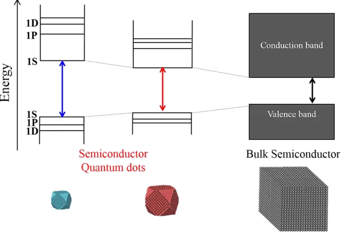
Semiconductor QDs are nm-scale spherical particles whose diameter is smaller than the exciton Bohr radius. In this size range, the electron and hole were confined along the three-dimensional direction, and the absorption and emission properties were strongly depends on the size of QDs (Figure 1.1).3,27,63 The latter is well known as “quantum size effect”, and can be described approximately by a “particle in a box” model. In addition to size-dependent optical properties, the electronic structure in QDs becomes discrete while the bulk semiconductor have the continuous band structure (Figure 1.1). Notations of discrete electronic states in QDs in order of increasing the energy are 1S, 1P, and 1D, and the energy
6
spacing between 1S and 1P states is especially large as compared with the phonon energy.27,64,65 These discrete energy states lead to the drastic change of hot carrier relaxation processes in semiconductor QDs.29,33,66 Furthermore, the strong spacial confinement of electron and hole in QDs induced the enhancement of carrier-carrier Coulomb interaction. This effect leads to the efficient MEG process and annihilation of multiexciton such as Auger recombination (Figure 1.2).36-44 In addition, the strong Coulomb interaction leads to the unique and highly efficient electron transfer process from semiconductor QDs to acceptor molecules, where the Marcus inverted region does not exist.53
Previously, a great deal of researcher have prepared the semiconductor QDs by using “physical” or “chemical” methods. In physical methods, semiconductor QDs grow on the substrate using the molecular beam epitaxy and metalorganic chemical vapor deposition methods. Semiconductor QDs prepared by the physical processes have an advantage in terms of carrier extraction from QDs. However, manufacturing equipments for these QDs are very expensive and large. On the other hand, semiconductor QDs were also prepared using colloidal synthetic method. By using the chemical synthetic method, semiconductor QDs which are covered with the organic ligand layer are dispersed in the polar or nonpolar solvents. In contrast to semiconductor QDs prepared by physical methods, colloidal semiconductor QDs are easy to prepare and cheaper. In addition, colloidal semiconductor QDs are freestanding which is different from epitaxial QDs grown on the substrate, and have the good size dispersion.67,68
1.2.2 Shape control of semiconductor nanocrystals
As described in 1.2.1, spherical colloidal semiconductor QDs confines electron and hole along three dimensional directions. In addition to QDs, the elongated (NRs) and planer (NPLs) nanocrystals corresponding to the two and one dimensional quantum confinement
7
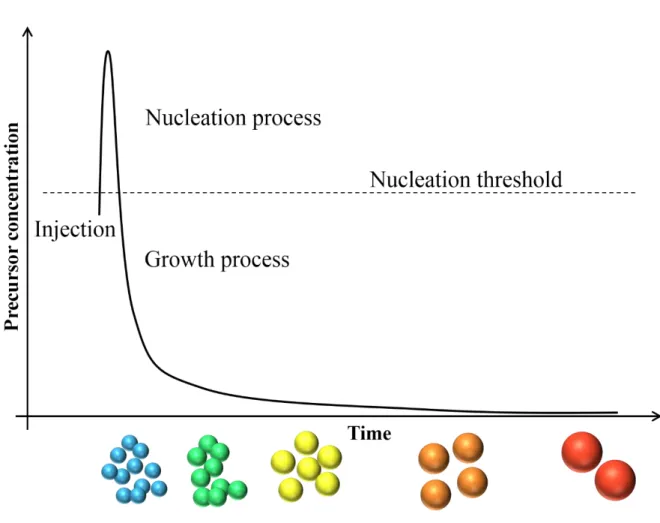
system have been synthesized by colloidal synthetic method.11,16 The general growth mechanism of colloidal semiconductor QDs was explained based on the previous study by La Mer and Dinegar.69 The high quality and monodisperse QDs can be synthesized by injecting organometallic precursor solution, such as Se-trioctylphosphine, to the coordinating solvent at high temperature (~300 °C).70 As shown in Figure 1.3, immediately after the precursor injection, the precursor concentration in the reaction mixture increases quickly over the nucleation threshold, and the concentration decreases rapidly by the formation of small nuclei which is the assembly of several precursors. When the precursor concentration became lower than the threshold of nucleation, the precursor reacts with the formed nuclei without the formation of new nuclei. After the further decrease of the precursor concentration by growing nuclei, the colloidal semiconductor QDs grow through the Ostwald ripening process, where smaller nanoparticle with the higher surface energy dissolved into the solution and larger nanoparticles further grow, and the concentration of nanoparticles decreases during the growth process.67,68,71
In addition to QDs, colloidal semiconductor nanocrystals elongated along one direction, which is called “nanorods (NRs)”, have been synthesized.11,14 Key factors for the
shape control of nanocrystals are the crystal structure, precursor concentration, and capping reagents.12,13,72 We describe the mechanism of shape control of CdSe nanocrystals as the
model system in the following sentences. In the CdSe nanocrystals, there are two possible crystal structures, zinc-blende and wurtzite structures. It is known that the crystals structures of nanocrystals can be controlled by the reaction temperature, where the wurtzite is the preferential structure at high temperature (thermodynamic phase) and the zinc-blende is the preferential structure at low temperature (kinetic phase).67,68 The wurtzite structure has the intrinsic anisotropy with the c/a ratio of ~1.6, although the zinc-blende is the cubic structure. In 2000, Peng et al. and Manna et al. have reported the one dimensional growth of wurtzite
8
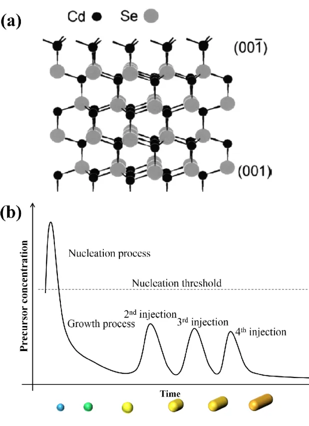
CdSe nanocrystals along the c-axis, which is capped with trioctylphosphine oxide and hexylphosphonic acid.11,12 In 2001, Z. A. Peng and X. Peng have revealed the anisotropic growth mechanism of CdSe NRs.13 Wrutzite CdSe NRs have two facets which are perpendicular to the c-axis, (001) and (001̅) facets, and these facets have different chemical compositions shown in Figure 1.4a. All atoms on both facet have a dangling bond, where (001) and (001̅) facets are terminated by positively charged Cd atoms and negatively charged Se atoms, respectively. Since the electron-donating ligand are used for the synthesis of CdSe NRs, the negatively charged (001̅) facet was not passivated by ligands, leading that (001̅) facet easily react with the Cd precursor in the solution. In addition, even if the Cd precursor react with the (001̅) facet, surface Cd atoms on the (001̅) facet have three dangling bonds different from Cd atoms on the (001) facet. Moreover, electron-donating ligands such as alkylphosphonic acid passivate the {110} facets on the side of NRs as well as (001) facet. As a results, the highly reactivity of (001̅) facet compared with the (001̅) facet and side facets induces the efficient one-dimensional growth of CdSe nanocrystals. Wang et al. reported that the aspect ratio of CdSe NRs could be controlled by the selection of ligands, where the phosphonic acid with longer alkyl chain lead to the lower aspect ratio of CdSe NRs.15
Furthermore, the precursor concentration during the growth process is the important factor for the anisotropic growth of colloidal semiconductor nanocrystals. Peng et al. observed that the growth kinetics of CdSe nanocrystals was strongly depend on the Cd precursor concentration during the growth process.13 Immediately after the nucleation, in the high Cd precursor
concentration region, the aspect ratio of CdSe nanocrystals increased as the Cd precursor in the solution decreased (the reaction time increased). In the middle Cd precursor concentration region, the aspect ratio did not change although the volume of CdSe nanocrystals increased, suggesting the three dimensional growth. Finally, in the low Cd precursor concentration region, the aspect ratio of CdSe nanocrystals decreased with increasing the reaction time
9
without the decrease of volume and concentration, indicating that the monomer likely moved on the surface of a crystals from c-axis to the other two dimensions. The precursor concentration dependence of the growth of CdSe nanocrystals suggests that effective one dimensional growth is induced by maintaining the high precursor concentration during the growth process as shown in Figure 1.4b. Actually, Shieh et al. synthesized the colloidal CdSe, CdS, and CdTe NRs by the multiple injection of precursor solution.14 This precursor concentration dependence of the growth kinetics was interpreted by the diffusion-controlled process. In the higher precursor concentration, the chemical potential in the bulk solution is much higher than that in the vicinity of each facets of wurtzite CdSe nanocrystals, leading the diffusion of precursors from bulk solution to the surrounding region of CdSe nanocrystals. As mentioned above, the (001̅) facet of wurtzite CdSe nanocrystals have the unique structural features. In addition, Blanton et al. observed the permanent dipole moment of CdSe nanocrystals along c-axis.73 The unique (001̅) facet and dipole moment along c-axis increases the chemical potential of the (001̅) facet compared with the other facets. Therefore, the growth rate along c-axis is much faster than that along the others, and CdSe nanocrystals preferentially grows along the c-axis. In the lower precursor concentration, the gradient of chemical potential between the bulk solution and each facets of CdSe nanocrystals decreases. The impact of this decrease significantly affects to the growth at the (001̅) facet compared with the other facets because of the high chemical potential of the (001̅) facet. The smaller gradient of chemical potential between bulk solution and the vicinity of (001̅) facet leads to the difficulty of precursor diffusion into the (001̅) facet. As a result, the higher growth rate and small diffusion of precursors at the facets along c-axis cancel each other, and CdSe nanocrystals grows along three dimensional directions.
Furthermore, in 2008, S. Ithurria and B. Dubertret reported the colloidal synthetic method of CdSe NPLs which corresponds to the quantum wells.16 After this report, the
10
colloidal synthesis of cadmium chalcogenide NPLs with various thicknesses and hetero-structure NPLs (core/shell and core/crown NPLs) are reported.19,23,24,74-76 Key factors for the two-dimensional growth of semiconductor nanocrystals are crystal structure and passivation by carboxylic acids ligands. In the synthesis of CdSe NPLs as a model system, the nucleation of CdSe seed crystals occurs at the relatively low temperature (<240 °C), leading the formation of the zinc-blende crystal structure of CdSe nanocrystals.74 In the zinc-blende CdSe NPLs, the thickness direction is confirmed to be [100] direction using the high resolution transmission electron microscopy, and perpendicular facets to the thickness direction (top and bottom facets) are {100} facets.74,77 The {100} facets of zinc-blende CdSe are terminated by cadmium atoms.19,78,79 Therefore, these facets of CdSe seed crystals are well
passivated by carboxylic acid ligands, which induces the prevention of the growth of CdSe seeds along the only thickness direction. Consequently, CdSe nanocrystals grow along two dimensional directions.
1.2.3 Electronic structures of semiconductor nanocrystals
As mentioned above, the semiconductor QDs (three dimensional quantum confinement system) have discrete electronic states while bulk semiconductors have the continuous band structures. In early studies, electron and hole which are strongly confined in QDs can be treated in the simple model, particle-in-a-sphere model, where wavefunctions of electron and hole are represented as the product of a spherical harmonic and a spherical Bessel function.80,81 In this model, the wavefunction can be described in the simple atomic-like orbital labeled by the angular momentum number (L) and radial quantum number (n), and energy levels in order of increasing energy is described as 1S, 1P, 1D, 2S, etc. Moreover, the first exciton band in the absorption spectrum of QDs is assigned to 1Sh-1Se
11
In the simple particle-in-a-sphere model, the conduction and valence band were approximated by simple parabolic bands. However, the actual band structure of II-VI semiconductors is more complicated. In the theoretical work which takes into account the valence band degeneracy and mixing of valence band, the total angular momentum F is appropriate quantum number for the label of the hole wavefunction. The total angular momentum F is sum of the Bloch-function angular momentum J and the orbital momentum of hole wavefunction Lh, F = J + Lh. Therefore, the hole states in the QDs are labeled as nhLF, although the electron states are not affected by the complexities of valence band and labeled as neLe. According to this theory, the lowest three absorption band observed in CdSe QDs can be assigned to 1S3/2-1Se, 2S3/2-1Se, and 1P3/2-1Pe (Figure 1.5).64,65,82
The quantum confinement dimensionality of semiconductor nanocrystals significantly affects the electronic structures. Hu et al. examined the aspect ratio dependent electronic structures of CdSe NRs (two dimensional quantum confinement system) by the semiempirical psuedopotential calculation.83 In this report, the additional electronic states
arising from the weak quantum confinement along the long axis generated between the discrete electronic states for QDs with the aspect ratio of 1, and the density of states increases with increasing the aspect ratio of CdSe NRs. According to this calculation, lowest three absorption band of CdSe NRs in Figure 1.6 can be assigned to transition of 1v-1c (1 band),
2v-2c (2 band), and 1v-1c (1 band).62
Furthermore, the recent progress in the colloidal synthesis of semiconductor nanocrystals allows us to synthesize the colloidal CdSe NPLs (one dimensional quantum confinement system) with the atomic-layer precision. These NPLs have very narrow absorption and emission bands arising from the small contribution of inhomogeneous broadening (size distribution) and coherent motion of the exciton.74,78,79 As shown in Figure
12
band (from heavy-hole band edge to conduction band-edge state) and light-hole band (from light-hole band edge to conduction band-edge state) similar to absorption bands of epitaxial quantum wells.16,74 In the theoretical work by Bose et al., first 10 electron levels exist in the range of few hundreds of meV, although the energy spacing between 1Se and 1Pe states in
QDs is a few hundreds of meV.84
1.2.4 Carrier dynamics of semiconductor nanocrystals
As mentioned above, colloidal semiconductor QDs exhibit the discrete energy state and enhancement of Coulomb interaction, which significantly affect to the hot carrier relaxation and single- and multi-exciton dynamics. The strong electron-hole Coulomb interaction in semiconductor nanocrystals enhance the probability of radiative recombination compared with the bulk semiconductors. However, in the semiconductor nanocrystals, the surface condition strongly affect to the nonradiative recombination process such as the carrier trapping at the surface defects.27 The carrier trapping to surface defect states can be
suppressed by the coating of the surface with different semiconductor shell.5,6 In addition to the single exciton dynamics, the multiexciton dynamics in semiconductor nanocrystals is different from bulk semiconductors. In the semiconductor QDs, multiple exciton annihilation process is dominated by the nonradiative Auger recombination with the lifetime of several tens of ps, which is a process that electron and hole recombine nonradiatively by the energy transfer to another carrier (electron or hole).27,63 The Auger recombination process in QDs is
significantly enhanced as compared to that in bulk because of the strong exciton-exciton interaction and relaxation of momentum conservation.85 In our group, Kobayashi et al
reported that the lifetime of Auger recombination in CdS QDs depends only on the size of QDs, which is irrespective of surface defects and ligands, and was proportional to ~D6 (D:
13
for CdTe QDs (D = ~4.0 nm) capped with oleic acids were examined using a streak camera.86 In this report, the biexciton Auger rate in CdTe QDs exhibited the moderate temperature dependence and is proportional to the natural logarithm of temperature, where the contribution of phonon probably have important role for the satisfaction of energy conservation. The theoretical study by Kim et al revealed that the logarithm temperature dependence of Auger recombination, which agree well with the experimental work by Kobayashi et al., can be interpreted in terms of electron-phonon coupling accompanied by Auger recombination.87 The multiple exciton annihilation dynamics can be modified by controlling the quantum confinement dimensionality. A.V. Barzykin and M. Tachiya analyzed the multiexciton Auger process in semiconductor nanocrystals using stochastic models.88 The
multiexciton Auger recombination process in QDs was analyzed by the three-particle model or two-particle model. In the three-particle model, electron and hole does not form an exciton because of the strong confinement energy and Auger recombination occurs between two electrons and one hole (or one electron and two holes). In this case, the multiexciton Auger recombination rate in the n exciton state (𝑘𝑛𝐴) is represented as 𝑘𝑛𝐴 = 12𝑛2(𝑛 − 1)𝑘2𝐴. On the
other hand, in the two-particle model, electron and hole are bound and form an exciton and Auger recombination occurs between two excitons. In this case, the 𝑘𝑛𝐴 is represented as
𝑘𝑛𝐴 = 12𝑛(𝑛 − 1)𝑘2𝐴. In the theoretical work by A.V. Barzykin and M. Tachiya, multiexciton
Auger recombination processes can be expressed by the two-particle (bimolecular) model rather than the three-particle model, since the average number of excitons per one QD is only a few. In the previous experimental studies, the higher order multiexciton Auger recombination process occurs with the three-particle process.89-91 Moreover, V. I. Klimov and
coworkers analyzed the multiexciton Auger recombination dynamics in CdSe QDs and NRs, and found the transition of the multiexciton Auger recombination process from three-particle process to bimolecular process with increasing the aspect ratio of CdSe NRs.89 This transition
14
of Auger recombination process was attributed to the formation of 1D exciton arising from the decrease of confinement energy and enhancement of Coulomb interaction.39,89,92 Considering the number of exciton (n) dependence of 𝑘𝑛𝐴, high order (n > 2) multiexciton Auger recombination in a bimolecular process is slower than that in a three-particle process. Actually, CdSe NRs exhibited the decrease of 𝜏2𝐴/ 𝜏3𝐴 and longer 𝜏3𝐴 as compared to the CdSe QDs, suggesting the bimolecular Auger recombination process in CdSe NRs. Moreover, Aerts et al. reported the similar transition of multiexciton annihilation process in PbSe QDs and NRs.90 In addition to the semiconductor NRs, Kunnemann et al. revealed that colloidal CdSe NPLs and CdSe/CdS/ZnS NPLs (one dimensional quantum confinement system) exhibited the significantly slow biexciton Auger recombination with the lifetime of ~10 ns and the bimolecular multiexciton annihilation process, suggesting the electron and hole form an exciton in semiconductor NPLs.93
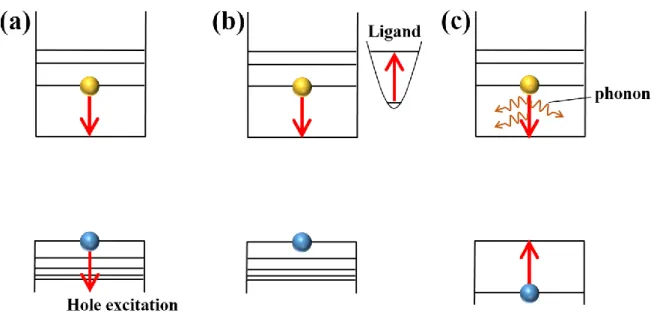
The hot electron and hole relaxation processes in colloidal semiconductor QDs is much different from that in bulk semiconductor because of discrete energy states in QDs as mentioned in 1.2.3. In the II-VI semiconductor nanocrystals such as CdSe QDs, since the energy spacing between 1Se and 1Pe states are especially large, which is 10 times larger than
the LO phonon energy of CdSe QDs (~ 30 meV), a hot electron cannot relaxed to the 1Se state
by the phonon emission in contrast with bulk semiconductors.27 In the previous studies, three
possible processes are proposed for the hot electron relaxation mechanism, which are Auger cooling, energy transfer to ligands and multiple phonon emission (Figure 1.8).29-34 First, the
Auger cooling process was proposed as the hot electron relaxation mechanism in CdSe QDs by Efros et al., where a hot electron relaxes from the 1Pe state to 1Se state through the transfer
of excess electron energy to a hole.28 The Auger cooling process can be very efficient in semiconductor QDs because of the large wavefunction overlap, enhanced electron-hole Coulomb interaction, and relaxation of momentum conservation.29 In the experimental works
15
by Klimov and coworkers, the Auger cooling process in CdSe QDs was examined using the femtosecond pump-prove spectroscopy.27,66,94 In their report, hot electron relaxation rates from 1Pe to 1Se state decreased as the size of CdSe QDs increased. Moreover, they compared
the hot electron relaxation dynamics of CdSe/ZnS QDs with that of CdSe QDs capped with pyridine (hole acceptor) and found that the hot electron transfer time became longer in pyridine-capped CdSe QDs (from ~320 fs to 3 ps), resulting from the reduction of electron-hole interaction by the spacial charge separation between CdSe QDs and pyridine molecules.27 This experimental result indicates the contribution of Auger cooling process to the hot electron relaxation. However, even in the charge separated CdSe QDs-pyridine system, the ps-scale hot electron relaxation time was much faster compared with the relaxation via phonon emission, suggesting the existence of other hot electron relaxation mechanism. Second, the role of surface ligands to the hot electron relaxation process was revealed by Gyot-Sionnest group. They examined the hot electron relaxation dynamics from 1Pe to 1Se
state in CdSe QDs with different surface ligands.33 According to their report, the hot electron
relaxation rate can be modified by changing surface ligands, and the 1Pe electron relaxes to
1Se state via energy transfer to high-frequency vibration of surface ligands. Furthermore,
Kambhampati group analyzed the hot electron and hole relaxation mechanism in CdSe QDs in more detail with the state-selective excitation experiments.29,31,32 They revealed that the
Auger cooling process and energy transfer to surface ligands contributed dominantly to the hot electron relaxation from 1Pe to 1Se and hot hole relaxation from 2Sh to 1Sh, respectively.
In II-VI semiconductor QDs, the Auger cooling process occurs effectively because of the higher density of states in valence band as compared to that in conduction band. On the other hand, IV-VI semiconductor QDs have a mirrorlike symmetry between conduction and valence band, leading the suppression of an Auger cooling process. Schaller et al. reported the clear temperature dependence of hot carrier relaxation from 1P-to-1S states in PbSe QDs, although
16
the hot electron relaxation time in CdSe QDs is independent of the temperature, suggesting the contribution of phonon.34 Therefore, they concluded that the hot carrier relaxation in PbSe QDs was due to the multiphonon emission process.These experimental results of intraband transition processes in semiconductor QDs indicates that the hot carrier relaxation time can be controlled by the charge separation, surface ligands, and temperature. Since the electronic structure of semiconductor nanocrystals are modified by the change of quantum confinement dimensionality, hot carrier relaxation dynamics in NRs and NPLs can be different from that in QDs. Nevertheless, in contrast to semiconductor QDs, the hot electron and hole relaxation mechanism in semiconductor NRs and NPLs are still not established. Yu et al. examined the hot electron relaxation in CdSe NRs with thin (2.2 nm) and thick (7.2 nm) short axes.95 They
reported that hot electron relaxation rates of CdSe NRs were similar or slower than those of CdSe QDs, and the hot electron relaxation rate of thinner CdSe NRs (~3.2 eV/ps) is faster than that of thicker CdSe NRs (~0.39 eV/ps). The latter suggested that the dominant hot electron relaxation mechanism in CdSe NRs was probably not the LO phonon emission. Moreover, Sipple et al. reported that the hot electron relaxation in colloidal CdSe NPLs occurred by the phonon emission via continuous conduction band arising from the weak confinement along lateral directions.96
1.3 Carrier transfer from semiconductor nanocrystals 1.3.1 Electron transfer in molecular chromophores
The electron transfer process is one of the most basic and important chemical reaction. In 1956, R. A. Marcus reported the theoretical equation of the electron transfer between donor and acceptor molecules in polar solvent.48,49 In the Marcus theory, the electron transfer rate (kET) was derived based on the transition state theory as following equation,
17 𝑘𝐸𝑇 = 𝑍𝑒𝑥𝑝(−∆𝐺
∗
𝑘𝐵𝑇) (1)
where Z is the frequency factor, kB is the boltzmann constant. G* is the activation energy of electron transfer reaction (shown in Figure 1.9) which is represented as following equation,
∆𝐺∗ =(ΔG+𝜆)
2
4𝜆 (2)
where G is the change in Gibbs energy corresponding the energy difference between the
initial state and final state. is the reorganization energy which corresponds to the energy required to change the orientation of solvent molecules for the stabilization of the products, and represented as below,
λ = 𝑒 2 4𝜋𝜀0( 1 2𝑎𝐷+ 1 2𝑎𝐴− 1 𝑟𝐷𝐴) ( 1 𝜀𝑜𝑝− 1 𝜀𝑠) (3)
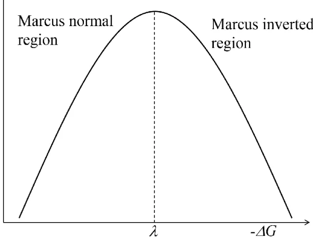
where aD and aA are radius of donor and acceptor molecules, rDA is the distance between donor and acceptor molecules, op and s are optical and static dielectric constant of the solvent. The remarkable point of the equation in Marcus theory is the energy gap law of electron transfer rate, where the electron transfer rate reaches the maximum value at –G =
and decreases with increasing the –G (> ) which is well known as the ”Marcus inverted region” (Figure 1.10). After this report, the validity of Marcus theory was proven experimentally by Miller et al in 1984.50,97 They examined the correlation between –G and
electron transfer rate from the biphenyl anion radical to the several kinds of acceptor molecule, where the donor and acceptor molecules were connected with a rigid saturated hydrocarbon spacer. In that experiment, the decrease of electron transfer rate as the –G increased were
18
clearly observed, revealing the existence of the Marcus inverted region.
1.3.2 Electron transfer in semiconductor nanocrystals
The electron transfer from semiconductor nanocrystals to the outside (metal oxides, acceptor molecules, metal NPs, etc.) have been reported by various groups.51-62 Yang et al. examined electron transfer dynamics from PbS QDs to TiO2 NPs.58 In this system, the
existence of the ultrafast adiabatic electron transfer from the 1Se state of PbS QDs with the
lifetime of ~6 fs were suggested, resulting from strong mixing of electronic states of PbS QDs and TiO2 NPs. In addition, Sambur et al. reported the multiple exciton collection from PbS
QDs to single crystalline TiO2 using the photon-to-current efficiency measurements, where
the multiexciton were generated by a MEG process.59 The multiple electrons extraction was also observed in the semiconductor nanocrystal-acceptor molecules complexes. Matylitsky et al. reported ~4 electrons can be extracted from CdSe QDs to methyl viologen (electron acceptor, MV2+) adsorbed on the surface of QDs.51 In addition, the more efficient multiple
electron transfer was achieved in CdSe NR-MV2+ and CdSe/CdS core/shell QD-MV2+ complexes by controlling quantum confinement dimensionality and the electron and hole wavefunction, respectively.52,54 Moreover, the ultrafast electron transfer from the band-edge state in semiconductor-metal HNs were detected in CdS NR-Au HNs and PbS QD-Au HNs, suggesting the possibility of multi carrier collection in semiconductor-metal HNs.60,98
In addition to ultrafast electron transfer, as mentioned above, the hot electron transfer can potentially allow the increase of the photon-to-current conversion efficiency. Tisdale et al. reported the hot electron transfer from thiol-capped PbSe QDs to single crystalline TiO2 at
low temperature (~80 K).99 Zhu et al. and Wang et al. reported the hot electron transfer from CdSe NRs and CdSe QDs, respectively.54,100 In addition, in the our previous study on CdSe
19
pump-prove spectroscopy with the state-selective excitation technique.62,101 CdSe NR-Au HNs with the largest diameter of Au NPs (~2.2 nm) exhibited the hot electron transfer with the lifetime of ~0.5-1.0 ps and the highest hot electron transfer yield of ~23%.
Furthermore, a recent work by T. Lian and co-workers examined the energy gap law of electron transfer rate from band-edge state of cadmium chalcogenide (CdX) QDs to several kinds of acceptor molecules.53 They reported the unique and efficient electron transfer processes where the electron transfer rate monotonically increased with increasing the -G,
meaning the Marcus inverted region does not exist. As mentioned above, colloidal semiconductor QDs strongly confines electron and hole in itself, leading the enhancement of electron-hole Coulomb interaction. This enhancement affects the electron transfer process as well as the hot carrier relaxation and multiexciton dynamics in semiconductor nanocrystals. In the conventional electron transfer theory, the contribution of hole dynamics associated with electron transfer from QDs to acceptor molecules is neglected, where the product state is represented as QD+(1S
h)-A-. In contrast, Lian et al. consider that the excess electron energy is
conserved by the excitation of 1S hole to the deeper conduction band states (Eh,i) associated with the electron transfer, which is like an Auger cooling process, and there is a manifold of product state represented as QD+(Eh,i)-A-. In addition, authors further assumed that the electronic coupling constant depends not only on the overlap of 1Se state and acceptor orbital
but also on the electron-hole Coulomb interaction, and the density of hole states in the quasi-continuum valence band was represented by 𝜌ℎ(𝐸ℎ, 𝑅)𝑑𝐸ℎ ∝ 𝐸ℎ𝑅3 . In the
nonadiabatic limit, the total electron transfer rate (k’ET) from 1Se state of CdX QDs with the
radius of R to acceptor molecules accompanied with the 1S hole excitation can be represented by the following equation,
𝑘′𝐸𝑇(𝑅) = 𝐶|Ψ1𝑆𝑒(𝑅)0|2𝑅2∫ 𝑑𝐸 ℎ𝐸ℎ2𝜋ℏ √4𝜋𝜆𝑘1 𝐵𝑇𝑒𝑥𝑝 [− (𝜆+∆𝐺(𝑅)+𝐸ℎ)2 4𝜆𝑘𝐵𝑇 ] ∞ 𝐸ℎ=0 (4)
20 where 𝐶|Ψ1𝑆𝑒(𝑅)0|
2
represents the electronic coupling constant between QDs and acceptor molecules, which is represented as |𝐻̅(𝐸)| in the conventional electron transfer theory. The electronic coupling constant between QDs and acceptor molecules strongly depends on the 1S electron density at the surface of QDs (|Ψ1𝑆𝑒(𝑅)0|
2
). The C is the size independent factor that depends on the material of QDs and molecules. To more clearly illustrate the -G dependence
of electron transfer rate, the electron transfer rate (k’ET(R)) is divided by the size and material dependent factor. The scaled electron transfer rate (k’ET(-G)) is given in the following equation, 𝑘′𝐸𝑇(−∆𝐺) = ∫ 𝑑𝐸ℎ𝐸ℎ2𝜋ℏ √4𝜋𝜆𝑘1 𝐵𝑇𝑒𝑥𝑝 [− (𝜆+∆𝐺(𝑅)+𝐸ℎ)2 4𝜆𝑘𝐵𝑇 ] ∞ 𝐸ℎ=0 (5)
By using equation 4 and 5, the obtained size and -G dependence of the electron transfer rate
from CdX QDs to acceptor molecules can be well fitted. Therefore, the unique electron transfer processes in the semiconductor QDs are originated from the strong electron-hole Coulomb interaction in QDs and the excitation of 1S hole to the deeper valence band states. This novel efficient electron transfer process in semiconductor nanocrystals is named “Auger-assisted electron transfer”.
1.4 Outline of this thesis
In this thesis, basic photophysical properties of colloidal semiconductor nanocrystals, and the quantum confinement dimensionality effect on their properties are given in Chapter 1. Chapter 2 introduces synthetic methods of several kinds of colloidal semiconductor nanocrystals and semiconductor-metal hybrid nanostructures. In Chapter 3, electron transfer
21
dynamics from 1Se and higher excited states of CdSe/CdS core/shell QDs to MV2+ are
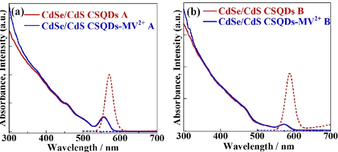
examined. From the analyses of transient absorption dynamics at 1S bleach band and MV+ radical band, hot electron transfer time in CdSe/CdS QDs with thicker shell is similar or slightly faster as compared to that in CdSe/CdS QDs with thinner shell in contrast with the shell thickness dependence of electron transfer from the 1Se state. Elementary electron
transfer processes from CdSe NPLs to MV2+ are discussed in Chapter 4. The lateral size dependence of electron transfer rate from band-edge state of CdSe NPLs to MV2+ reveals that the electron transfer rate depends on the CdSe NPLs face where MV2+ adsorbs on. In Chapter 5, carrier transfer dynamics in PbS QD-Au HNs were analyzed from initial bleach amplitude and relaxation dynamics at 1S bleach band. The ultrafast electron transfer whose lifetime is much faster than the instrumental response function (~60 fs) was observed in the 1S excitation experiments. In Chapter 6, we synthesized CdSe QD-Au HNs and examined electron transfer dynamics from 1Se state and higher excited states using the femtosecond
pump-probe spectroscopy. State-selective excitation experiments revealed that hot electron transfer occurred from 1Pe state whose lifetime and yields are estimated to be ~300 fs and
50%, respectively. Moreover, in 1S excitation experiments, the initial 1S bleach amplitude became lower with increasing the size of Au NPs, indicating the existence of ultrafast electron transfer from 1Se state. We compared the obtained results for CdSe QD-Au HNs to those for
CdSe NR-Au HNs. In addition, the electron transfer dynamics in CdSe NPL-Au HNs was discussed in Chapter 7. In contrast with CdSe QD-Au HNs, hot electron transfer and ultrafast electron transfer from band-edge state are not observed in CdSe NPL-Au HNs.
22
References
(1) Alfassi, Z.; Bahnemann, D.; Henglein, A. Photochemistry of colloidal metal sulfides. 3. Photoelectron emission from cadmium sulfide and cadmium sulfide-zinc sulfide cocolloids J. Phys. Chem., 1982, 86, 4656–4657.
(2) Rossetti, R.; Brus, L. Electron-hole recombination emission as a probe of surface chemistry in aqueous cadmium sulfide colloids J. Phys. Chem. 1982, 86, 4470–4472. (3) Rossetti, R.; Nakahara, S.; Brus, L. Quantum size effects in the redox potentials,
resonance Raman spectra, and electronic spectra of CdS crystallites in aqueous solution J.
Chem. Phys. 1983, 79, 1086–1088.
(4) Murray, C. B.; Norris, D. J.; Bawendi, M. G. Synthesis and characterization of nearly monodisperse CdE (E = sulfur, selenium, tellurium) semiconductor nanocrystallites. J. Am.
Chem. Soc. 1993, 115, 8706–8715.
(5) Peng, X.; Schlamp, M. C.; Kadavanich, A. V.; Alivisatos, A. P. Epitaxial Growth of Highly Luminescent CdSe/CdS Core/Shell Nanocrystals with Photostability and Electronic Accessibility J. Am. Chem. Soc. 1997, 119, 7019–7029.
(6) Dabbousi , B. O.; Rodriguez-Viejo, J.; Mikulec, F. V.; Heine, J. R.; Mattoussi, H.; Ober, R.; Jensen, K. F.; Bawendi, M. G. (CdSe)ZnS Core−Shell Quantum Dots: Synthesis and Characterization of a Size Series of Highly Luminescent Nanocrystallites. J. Phys. Chem.
23
(7) Talapn, D. V.; Koeppe, R.; Götzinger, S.; Kornowski, A.; Lupton, J. M.; Rogach, A. L.; Benson, O.; Feldmann, J.; Weller, H. Highly Emissive Colloidal CdSe/CdS Heterostructures of Mixed Dimensionality. Nano Lett. 2003, 3, 1677–1681.
(8) Müller, J.; Lupton, J. M.; Lagoudakis, P. G.; Koeppe, R.; Rogach, A. L.; Feldmann, J.; Talapn, D. V.; Weller, H. Wave Function Engineering in Elongated Semiconductor Nanocrystals with Heterogeneous Carrier Confinement. Nano Lett. 2005, 5, pp 2044–2049.
(9) Chuang, C.-H.; Lo, S. S.; Scholes, G. D.; Burda, C. Charge Separation and Recombination in CdTe/CdSe Core/Shell Nanocrystals as a Function of Shell Coverage: Probing the Onset of the Quasi Type-II Regime. J. Phys. Chem. Lett. 2010, 1, 2530–2535.
(10) Kim, S.; Brent, F.; Eisler, H.-J. Bawendi, M. Type-II Quantum Dots: CdTe/CdSe(Core/Shell) and CdSe/ZnTe(Core/Shell) Heterostructures. J. Am. Chem. Soc.
2003, 125, 11466–11467.
(11) Peng, X.; Manna, L.; Yang, W.; Wickham, J.; Scher, E.; Kadavanich, A.; Alivisatos, A. P. Shape control of CdSe nanocrystals. Science, 2000, 404, 59–61.
(12) Manna, L.; Scher, E. C.; Alivisatos, P. A. Synthesis of Soluble and Processable Rod-, Arrow-, Teardrop-, and Tetrapod-Shaped CdSe Nanocrystals. J. Am. Chem. Soc. 2000,
122, 12700–12706.
24
Am. Chem. Soc. 2001, 123, 1389–1395.
(14) Shieh, F.; Saunders, A. E.; Korgel, B. A. General Shape Control of Colloidal CdS, CdSe, CdTe Quantum Rods and Quantum Rod Heterostructures. J. Phys. Chem. B, 2005, 109, 8538–8542.
(15) Wang, W.; Banerjee, S.; Jia, S.; Steigerwald, M. L.; Herman, I. P. Ligand Control of Growth, Morphology, and Capping Structure of Colloidal CdSe Nanorods. Chem. Mater.
2007, 19, 2573–2580.
(16) Ithurria, S.; Dubertret, B. Quasi 2D Colloidal CdSe Platelets with Thicknesses Controlled at the Atomic Level. J. Am. Chem. Soc. 2008, 130, 16504−16505.
(17) Lhuillier, E.; Pedetti, S.; Ithurria, S.; Nadal, B.; Heuclin, H.; Dubertret, B. Two-Dimensional Colloidal Metal Chalcogenides Semiconductors: Synthesis, Spectroscopy, and Applications. Acc. Chem. Res. 2015, 48, 22−30.
(18) Tessier, M. D.; Javaux, C.; Maksimovic, I.; Loriette, V.; Dubertret, B. Spectroscopy of Single CdSe Nanoplatelets. ACS Nano 2012, 6, 6751–6758.
(19) Mahler, B.; Nadal, B.; Bouet, C.; Patriarche, G.; Dubertret, B. Core/Shell Colloidal Semiconductor Nanoplatelets. J. Am. Chem. Soc. 2012, 134, 18591–18598.
(20) She, C.; Fedin, I.; Dolzhnikov, D. S.; Dahlberg, P. D.; Engel, G. S.; Schaller, R. D.; Talapin, D. V. Red, Yellow, Green, and Blue Amplified Spontaneous Emission and Lasing Using Colloidal CdSe Nanoplatelets. ACS Nano 2015, 9, 9475−9485.
25
(21) Ithurria, S.; Tessier, M. D.; Mahler, B.; Lobo, R. P. S. M.; Dubertret, B.; Efros, Al. L. Colloidal Nanoplatelets with Two−dimensional Electronic Structure. Nat. Mater. 2011, 10, 936−941.
(22) Pelton, M.; Ithurria, S.; Schaller, R. D.; Dolzhnikov, D. S.; Talapin, D. V. Carrier Cooling in Colloidal Quantum Wells. Nano Lett. 2012, 12, 6158−6163.
(23) Tessier, M. D.; Spinicelli, P.; dupont, D.; Patriarche, G.; Ithurria, S.; Dubertret B. Efficient Exciton Concentrators Built from Colloidal Core/Crown CdSe/CdS Semiconductor Nanoplatelets. Nano Lett., 2014, 14, 207−213.
(24) Pedetti, S.; Ithurria, S.; Heuclin, H.; Patriarche, G.; Dubertret, B. Type−II CdSe/CdTe Core/Crown Semiconductor Nanoplatelets. J. Am. Chem. Soc. 2014, 136, 16430−16438.
(25) Mokari, T.; Rothenberg, E.; Popov, I.; Costi, R.; Banin, U. Selective Growth of Metal Tips onto Semiconductor Quantum Rods and Tetrapods. Science 2004, 304, 1787−1790.
(26) Mokari, T.; Sztrum, C. G.; Salant, A. Rabani, E.; Banin, U. Formation of Asymmetric One-sided Metal-tipped Semiconductor Nanocrystal Dots and Rods. Nat.
Mater. 2005, 4, 855−863.
(27) Klimov, V. I. Optical Nonlinearities and Ultrafast Carrier Dynamics in Semiconductor Nanocrystals. J. Phys. Chem. B 2000, 104, 6112−6123.
26
(28) Efros, A. L.; Kharchenko, V. A.; Rosen, M. Breaking the Phonon Bottleneck in Nanometer Quantum Dots: Role of Auger-like Process. Solid State Communication 1995,
93, 281−284.
(29) Kambhampati, P. Hot Exciton Relaxation Dynamics in Semiconductor Quantum Dots: Radiationless Transitions on the Nanoscale. J. Phys. Chem. C 2011, 115, 22089−22109.
(30) Kambhampati, P. Unraveling the Structure and Dynamics of Excitons in Semiconductor Quantum Dots. Acc. Chem. Res. 2011, 44, 1−13.
(31) Sewall, S. L.; Cooney, R. R.; Anderson, K. E. H.; Dias, E. A.; Kambhampati, P. State-to-State Exciton Dynamics in Semiconductor Quantum Dots. Phys. Rev. B 2006, 74, 235328.
(32) Cooney, R. R.; Sewall, S. L.; Dias, E. A.; Sagar, D. M.; Anderson, K. E. H.; Kambhampati, P. Unified Picture of Electron and Hole Relaxation Pathways in Semiconductor Quantum Dots. Phys. Rev. B 2007, 75, 245311.
(33) Guyot−Sionnest, P.; Wehrenberg, B.; Yu, D. Intraband Relaxation in CdSe Nanocrystals and the Strong Influence of the Surface Ligands. J. Chem. Phys. 2005, 123, 074709.
(34) Schaller, R. D.; Pietryga, J. M.; Goupalov, S. V.; Petruska, M. A.; Ivanov, S. A.; Klimov, V. I. Breaking the Phonon Bottleneck in Semiconductor Nanocrystals via
27
Multiphonon Emission Induced by Intrinsic Nonadiabatic Interactions. Phys. Rev. Lett.
2005, 95, 196401.
(35) Pandey, A.; Guyot-Sionnest, P. Slow Electron Cooling in Colloidal Quantum Dots.
Science 2008, 322, 929−932.
(36) Schaller, R. D.; Klimov, V. I. High Efficiency Carrier Multiplication in PbSe Nanocrystals: Implications for Solar Energy Conversion. Phys. Rev. Lett. 2004, 92, 186601.
(37) Scheller, R. D.; Petruska, M. A.; Klimov, V. I. Effect of Electronic Structure on Carrier Multiplication Efficiency: Comparative Study of PbSe and CdSe Nanocrystals.
Appl. Phys. Lett. 2005, 87, 253102.
(38) Scheller, R. D.; Pietryga, J. M.; Klimov, V. I. Carrier Multiplication in InAs Nanocrystal Quantum Dots with an Onset Defined by the Energy Conservation Limit.
Nano Lett. 2007, 7, 3469−3476.
(39) Padilha, L. A.; Stewart, J. T.; Sandberg, R. L.; Bae, W. K.; Koh, W.-K.; Pietryga, J. M.; Klimov, V. I. Aspect Ratio Dependence of Auger Recombination and CarrierMultiplication in PbSe Nanorods. Nano Lett., 2013, 13, 1092–1099.
(40) Stewart, J. T.; Padilha, L. A.; Bae, W. K.; Koh, W.-K.; Pietryga, J. M.; Klimov, V. I. Carrier Multiplication in Quantum Dots within the Framework of Two Competing Energy Relaxation Mechanisms. J. Phys. Chem. Lett. 2013, 4, 2061–2068.
28
(41) Kobayashi, Y.; Udagawa, T.; Tamai, N. Carrier Multiplication in CdTe Quantum Dots by Single−Photon Timing Spectroscopy. Chem. Lett. 2009, 38, 830−831.
(42) Klimov, V. I.; Mikhailovsky, A. A.; McBranch, D. W.; Leatherdale, C. A.; Bawendi, M. G. Quantization of Multiparticle Auger Rates in Semiconductor Quantum Dots.
Science 2000, 287, 1011−1013.
(43) Kobayashi, Y.; Pan, L.; Tamai, N. Effects of Size and Capping Reagents on Biexciton Auger Recombination Dynamics of CdTe Quantum Dots. J. Phys. Chem. C,
2009, 113, 11783–11789.
(44) Kobayashi, Y.; Nishimura, T.; Yamagushi, H.; Tamai, N. Effect of Surface Defects on Auger Recombination in Colloidal CdS Quantum Dots. J. Phys. Chem. Lett., 2011, 2, 1051–1055.
(45) Stewart, J. T.; Padilha, L. A.; Qazilbash, M. M.; Pietryga, J. M.; Midgett, A. G.; Luther, J. M.; Beard, M. C.; Nozik, A. J.; Klimov, V. I. Comparison of Carrier Multiplication Yields in PbS and PbSe Nanocrystals: The Role of Competing Energy-Loss Processes. Nano Lett. 2012, 12, 622−628.
(46) Shockley, W.; Queisser, H. J. Detailed Balance Limit of Efficiency of p−n Junction Solar Cells. J. Appl. Phys. 1961, 32, 510−519.
(47) Ross, R. T.; Nozik, A. J. Efficiency of hot−carrier solar energy converters. J. Appl.
29
(48) Marcus, R. A. On the Theory of Oxidation−Reduction Reactions Involving Electron Transfer. I. J. Chem. Phys. 1956, 24, 966−978.
(49) Marcus, R. A. Electrostatic Free Energy and Other Properties of States Having Nonequilibrium Polarization. I. J. Chem. Phys. 1956, 24, 979−989.
(50) Miller, J. R.; Calcaterra, L. T.; Closs, G. L. Intramolecular Long-Distance Electron Transfer in Radical Anions. The Effects of Free Energy and Solvent on the Reaction Rates.
J. Am. Chem. Soc. 1984, 106, 3047–3049.
(51) Matylitsky, V. V.; Dworak, L.; Breus, V. V.; Basché, T.; Wachtveitl, J. Ultrafast Charge Separation in Multiexcited CdSe Quantum Dots Mediated by Adsorbed Electron Acceptors. J. Am. Chem. Soc. 2009, 131, 2424–2425.
(52) Zhu, H.; Song, N.; Rodríguez–Córdoba, W.; Lian, T. Wave Function Engineering for Efficient Extraction of up to Nineteen Electrons from One CdSe/CdS Quasi–Type II Quantum Dot. J. Am. Chem. Soc. 2012, 134, 4250–4257.
(53) Zhu, H.; Yang, Y.; Hyeon−Deuk, K.; Califano, M.; Song, N.; Wang, Y.; Zhang, W.; Prezhdo, O. V.; Lian, T. Auger−Assisted Electron Transfer from Photoexcited Semiconductor Quantum Dots. Nano Lett. 2014, 14, 1263−1269.
(54) Zhu, H.; Lian, T. Enhanced Multiple Exciton Dissociation from CdSe Quantum Rods: The Effect of Nanocrystal Shape. J. Am. Chem. Soc. 2012, 134, 11289−11297. (55) Zhu, H.; Song, N.; Lian, T. Controlling Charge Separation and Recombination Rates
30
in CdSe/ZnS Type I Core−Shell Quantum Dots by Shell Thicknesses. J. Am. Chem. Soc.
2010, 132, 15038−15045.
(56) Yang, Y.; Rodríguez–Córdoba, W.; Lian, T. Multiple Exciton Generation and Dissociation in PbS Quantum Dot–Electron Acceptor Complexes. Nano Lett., 2012, 12, 4235–4241.
(57) Tisdale, W. A.; Zhu, X. Y. Artificial Atoms on Semiconductor Surfaces. Proc. Natl.
Acad. Sci. U. S. A. 2011, 108, 965−970.
(58) Yang, Y.; Rodríguez−Córdoba, W.; Xiang, X.; Lian, T. Strong Electronic Coupling and Ultrafast Electron Transfer between PbS Quantum Dots and TiO2 Nanocrystalline
Films. Nano Lett. 2012, 12, 303−309.
(59) Sambur, J. B.; Novet, T.; Parkinson, B. A. Multiple Exciton Collection in a Sensitized Photovoltaic System. Science 2010, 330, 63−66.
(60) Mongin, D.; Shaviv, E.; Maioli, P.; Crut, A. Banin, U.; Fatti, N. D.; Vallée, F. Ultrafast Photoinduced Charge Separation in Metal–Semiconductor Nanohybrids. ACS
Nano 2012, 6, 7034–7043.
(61) Wu, K.; Li, Q.; Du, Y.; Chen, Z.; Lian, T. Ultrafast Exciton Quenching by Energy and Electron Transfer in Colloidal CdSe Nanosheet−Pt Heterostructures. Chem. Sci. 2015,
6, 1049−1054.
31
Tamai, N. Ultrafast Dynamics and Single Particle Spectroscopy of Au–CdSe Nanorods.
Phys. Chem. Chem. Phys. 2013, 15, 2141–2152.
(63) Klimov, V. I. Spectral and Dynamical Properties of Multiexcitons in Semiconductor Nanocrystals. Annu Rev Phys Chem. 2007, 58, 635–673.
(64) Efros, A. L.; Rosen, M. The Electronic Structure of Semiconductor Nanocrystals.
Annu Rev Phys Chem. 2000, 30, 475–521.
(65) Norris, D. J.; Bawendi, M. G. Measurement and Assignment of the Size-dependent Optical Spectrum in CdSe Quantum Dots. Phys. Rev. B 1996, 53, 16338–16346.
(66) Klimov, V. I.; McBranch, D. W. Femtosecond 1P-to-1S Electron Relaxation in Strongly Confined Semiconductor Nanocrystals. Phys. Rev. Lett. 1998, 80, 4028–4031. (67) Klimov, V. I. Nanocrystal Quantum Dots Second Edition. CRC Press 2010.
(68) Klimov, V. I. Semiconductor and Metal Nanocrystals: Synthesis and Electronic and Optical Properties CRC Press 2003.
(69) La Mer, V. K.; Dinegar, R. H. Theory, Production and Mechanism of Formation of Monodispersed Hydrosols. J. Am. Chem. Soc. 1950, 72, 4847.
(70) Qu, L.; Peng, Z. A.; Peng, X. Alternative Routes toward High Quality CdSe Nanocrystals. Nano Lett., 2001, 1, 333–337.
(71) Murray, C. B.; Kagan, C. R. Bawendi, M. G. Synthesis and Characterization of Monodisperse Nanocrystals and Close-Packed Nanocrystal Assemblies. Annu Rev Phys
32
Chem. 2000, 30, 545–610.
(72) Nasilowski, M.; Mahler, B.; Lhuillier, E.; Ithurria, S.; Dubertret, B. Two-Dimensional Colloidal Nanocrystals. Chem. Rev. 2016, 116, 10934–10982.
(73) Blanton, S. A.; Leheny, R. L.; Hines, M. A.; Guyot-Sionnest, P Dielectric Dispersion Measurements of CdSe Nanocrystal Colloids: Observation of a Permanent Dipole Moment. Phys. Rev. Lett. 1997, 79, 865–868.
(74) Ithurria, S.; Tessier, M. D.; Mahler, B.; Lobo, R. P. S. M.; Dubertret, B.; Efros, Al. L. Colloidal Nanoplatelets with Two−dimensional Electronic Structure. Nat. Mater. 2011, 10, 936−941.
(75) Prudnikau, A.; Chuvilin, A.; Artemyev, M. CdSe−CdS Nanoheteroplatelets with Efficient Photoexcitation of Central CdSe Region through Epitaxially Grown CdS Wings.
J. Am. Chem. Soc. 2013, 135, 14476−14479.
(76) Delikanli, S.; Guzelturk, B.; Hernández-Martínez, P. L.; Erdem, T.; Kelestemur, Y.; Olutas, M.; Akgul, M. Z.; Demir, H. V. Continuously Tunable Emission in Inverted Type-I CdS/CdSe Core/Crown Semiconductor Nanoplatelets. Adv. Funct. Mater. 2015, 25, 4282−4289.
(77) Ithurria, S.; Bousquet, G.; Dubertret, B. Continuous Transition from 3D to 1D Confinement Observed during the Formation of CdSe Nanoplatelets. J. Am. Chem. Soc.
33
(78) Bouet, C.; Tessier, M. D.; Ithurria, S.; Mahler, B.; Nadal, B.; Dubertret, B. Flat Colloidal Semiconductor Nanoplatelets. Chem. Mater. 2013, 25, 1262–1271.
(79) She, C.; Fedin, I.; Dolzhnikov, D. S.; Demortière, A.; Schaller, R. D.; Pelton, M.; Talapin, D. V. Low-Threshold Stimulated Emission Using Colloidal Quantum Wells.
Nano Lett. 2014, 14, 2772–2777.
(80) Efros, A. L.; Efros, A. L. Interband Absorption of Light in a Semiconductor Sphere.
Sov. Phys. Semicond. 1982, 16, 772–775.
(81) Brus, L. E. Electron–electron and Electron–hole Interactions in Small Semiconductor Crystallites: The Size Dependence of the Lowest Excited Electronic State. J. Chem. Phys.
1984, 80, 4403–4409.
(82) Ekimov, A. I.; Hache, F.; Schanne-Klein, M. C.; Ricard, D.; Flytzanis, C.; Kudryavtsev, I. A.; Yazeva, T. V.; Rodina, A. V. Efros, A. L. Absorption and Intensity-dependent Photoluminescence Measurements on CdSe Quantum Dots Assignment of the First Electronic Transitions. J. Opt. Soc. Am. B 1998, 10, 100–107. (83) Hu, J.; Lin, W.; Liang, S. L.; Yang, W.; Alivisatos, A. P Semiempirical
Pseudopotential Calculation of Electronic States of CdSe Quantum Rods. J. Phys. Chem.
B, 2002, 106, 2447–2452.
(84) Bose, S.; Song, Z.; Fan, W. J.; Zhang, D. H. Effect of Lateral Size and Thickness on the Electronic Structure and Optical Properties of Quasi Two-dimensional CdSe and CdS
34 Nanoplatelets. J. Appl. Phys. 2016, 119, 143107.
(85) Klimov, V. I.; McGuire, J. A.; Schaller, R. D.; Rupasov, V. I. Scaling of multiexciton lifetimes in semiconductor nanocrystals. Phys. Rev. B 2008, 77, 195324.
(86) Kobayashi, Y.; Tamai, N. Size-Dependent Multiexciton Spectroscopy and Moderate Temperature Dependence of Biexciton Auger Recombination in Colloidal CdTe Quantum Dots. J. Phys. Chem. C 2010, 114, 17550–17556.
(87) Heyon–Deuk, K.; Kobayashi, Y.; Tamai, N. Evidence of Phonon-Assisted Auger Recombination and Multiple Exciton Generation in Semiconductor Quantum Dots Revealed by Temperature-Dependent Phonon Dynamics. J. Phys. Chem. Lett. 2014, 5, 99–105.
(88) Barzykin, A. V.; Tachiya, M. Stochastic models of charge carrier dynamics in semiconducting nanosystems. J. Phys.: Condens. Matter. 2007, 19, 065105.
(89) Htoon, H.; Hollingsworth, J. A.; Dickerson, R.; Klimov, V. I.; Effect of Zero- to One-Dimensional Transformation on Multiparticle Auger Recombination in Semiconductor Quantum Rods Scaling of multiexciton lifetimes in semiconductor nanocrystals. Phys. Rev. Lett. 2003, 91, 227401.
(90) Aerts, M.; Spoor, F. C. M.; Grozema, F. C.; Houtepen, A. J.; Schins, J. M.; Siebbeles, L. D. A. Cooling and Auger Recombination of Charges in PbSe Nanorods: Crossover from Cubic to Bimolecular Decay. Nano Lett. 2013, 13, 4380–4386.
35
(91) Ueda, A.; Tayagaki, T.; Kanemitsu, Y. Dynamics of Quantized Auger Recombination in CdSe Nanocrystals Studied by Femtosecond Intraband Pump–Probe Spectroscopy. J. Phys. Soc. Jpn. 2009, 78, 083706.
(92) Bartnik, A. C.; Efros, A. L.; Koh, W.-K.; Murray, C. B.; Wise, F. W. Electronic States and Optical Properties of PbSe Nanorods and Nanowires. Phys. Rev. B 2010, 82, 195313.
(93) Kunneman, L. T.; Tessier, M. D.; Heuclin, H.; Dubertret, B; Aulin, Y. V.; Grozema, F. C.; Schins, J. M.; Siebbeles, L. D. A. Bimolecular Auger Recombination of Electron−Hole Pairs in Two-Dimensional CdSe and CdSe/CdZnS Core/Shell Nanoplatelets. J. Phys. Chem. Lett. 2013, 4, 3574–3578.
(94) Klimov, V. I.; McBranch, D. W.; Leatherdale, C. A.; Bawendi M. G. Electron and Hole Relaxation Pathways in Semiconductor Quantum Dots. Phys. Rev. B 1999, 60, 13740.
(95) Yu, P.; Nedeljkovic, J. M.; Ahrenkiel, P. A.; Ellingson, R. J.; Nozik, A. J. Size Dependent Femtosecond Electron Cooling Dynamics in CdSe Quantum Rods. Nano Lett.
2004, 4, 1089–1092.
(96) Sippel, P.; Albrecht, W.; Bok, J. C.; Dijk-Moes, R. J. A.; Hannappel, T.; Eichberger, R.; Vanmaekelbergh, D. Femtosecond Cooling of Hot Electrons in CdSe Quantum-Well Platelets. Nano Lett. 2015, 15, 2409–2416.
36
(97) Miller, J. R.; Beitz, J. V.; Huddleston, R. K. Effect of Free Energy on Rates of Electron Transfer between Molecules. J. Am. Chem. Soc. 1984, 106, 5057–5068.
(98) Okuhata, T.; Kobayashi, Y.; Nonoguchi, Y.; Kawai, T.; Tamai, N. Ultrafast Carrier Transfer and Hot Carrier Dynamics in PbS−Au Hybrid Nanostructures. J. Phys. Chem. C
2015, 119, 2113–2120.
(99) Tisdale, W. A.; Williams, K. J.; Timp, B. A.; Norris, D. J.; Aydil, E. S.; Zhu, X.-Y. Hot−Electron Transfer from Semiconductor Nanocrystals. Science 2010, 328, 1543−1547. (100) Wang, Y.; Wang, H.; Li, Z.; Zhao, J.; Wang, L.; Chen, Q.; Wang, W.; Sun, H. Electron Extraction Dynamics in CdSe and CdSe/CdS/ZnS Quantum Dots Adsorbed with Methyl Viologen. J. Phys. Chem. C 2014, 118, 17240−17246.
(101) Sagarzazu, G.; Inoue, K.; Saruyama, M.; Sakamoto, M.; Teranishi, T.; Tamai, N. Hot-electron transfer in Au-CdSe nanorods. Submitted.
37
Figure 1.1 Size dependent electronic structures of semiconductor QDs and the band structure of bulk semiconductors.
38
Figure 1.2 Schemes of the (a) multiple exciton generation process and (b) Auger recombination process.
39
Figure 1.3 The scheme for a nucleation and growth of colloidal semiconductor nanocrystals based on La Mer’s model.
40
Figure 1.4 (a) The crystal structure of wrutzite CdSe12 and (b) the scheme of anisotropic
41
Figure 1.5 (a) The energy diagram and optical transitions of CdSe QDs and (b) absorption spectrum of typical CdSe QDs.
42
Figure 1.6 (a) The calculated electronic structure of CdSe nanocrystals with different aspect ratio83 and (b) absorption spectrum of typical CdSe NRs.