TABLE IV inputand r product lines, (n + 2)r + 2 test patterns are necessary THECOMPLETE PLA TEST PROGRAM (excluding shift register tests).
PROGRAM TEST; ACKNOWLEDGMENT
BEGIN The author gratefully acknowledges the support and guidance
zero; one; two; three
provided
by Prof. E. J. McCluskey andDr.
D. J. Lu.END.
REFERENCES
TABLE V [1] H. Fujiwara, K. Kinoshita, and H. Ozaki, "Universal test sets for pro- ANEXAMPLE grammable logic arrays," in Dig.10thAnnu. Int.Symp. Fault-Tolerant Correct output Computing (FTCS-10), Kyoto, Japan, Oct. 1-3, 1980, pp. 137-142. Input patterns response [2] H.Fujiwaraand K. Kinoshita,"Adesignofprogrammable logicarrays Procedure s1 s2 s3 s4 x1 x2 z 1z 2 andwith universal tests,", IEEE Trans.IEEECircuitsTrans.Syst., vol. CAS-28, pp. 1027-1032,Comput., vol. C-30, pp. 823-828;
ZERO see note 1 below Nov. 1981.
o 1 1 1 1 1 1 [31 G.D. Hachtel, A. R. Newton, and A. L. Sangiovanni-Vincentelli, "An
1 1 1 1 1 1 0 algorithmforoptimalPLAfolding,"IEEE Trans.Comput. Aided Design ONE 1 1 1 1 1 1 0 - - Integrated Circuits Syst., vol. CAD-1, no. 2, pp. 63-77, Apr. 1982. 1 1 1 1 9 1 O - - [4] G. D. Hachtel, "Techniques for programmable logic array folding," in 1 111 11 11 0 01 0 0 - - 0--pp4-15
Proc.
19thDesign
Automat. Conj., Las Vegas,NV.
June 14-16, 1982, TWO 0 1 1 1 1 1 1 1 0 [5] S. J. Hong and D. L. Ostapko,"FITPLA: A programmable logic array for& 0O11 11 11 0 11 0 00 - -
function-independent testing,"
inDig.
10th Annu. Int. Symp. Fault-Tolerant Computing (FTCS-10), Kyoto, Japan, Oct. 1-3, 1980,
THREE 1 0 1 1 0 1 1 0 Toeat(TS])1c.13 90
1 0 1 1 ; 1 1 - - pp. 131-136.
1 0 1 1 9 0 0 - - [6] J. Khakbaz, "A testable PLA design with low overhead and high 1 1 0 1 0 0 fault coverage," Center for Reliable Computing, Comput. Syst. Lab.,
1 1 o 1 1 9 1 Dep. Elec. Eng., Stanford Univ., Stanford, CA, CRC Rep. 82-17
1 1 1 0 0 0 1 0 (CSL TN216),Oct. 1982.
1 1 1 0 1 0 0 - -
[7]
C.Meadand L. Conway,Introductionto VLSI Systems. Reading, MA:1 1 1 0 0 1 0 - - Addison-Wesley, 1980.
NOTES: 1 Test patterns for shift register [8] K. K. Saluja, K. Kinoshita, and H. Fujiwara,"Amultiplefault testable are not shown. (see Proc. ZERO.) design ofprogrammable logic arrays," in Dig. Ilth Annu. Int. Symp. 2. - denotes don't-care output; Fault-Tolerant Computing(FTCS-1l),Portland, ME,June24-26,
1981,
9 denotes 0 for don't-care input pp.44-46.
variable; denotes 1 for [9] R.A.
Wood, "A high density programmable logic array chip,"IEEE don't-care input variable.
Trans. Comput., vol.C-28, pp. 602-608, Sept. 1979.
[10] S. Yajima and T. Aramaki, "Autonomously testable programmable for every
product
line in the PLA. PROCEDURE TWO in Table II. logic arrays,"inDig. 11th Annu.Init.
Svmp.Fault-TolerantComputing describes this stage of thetest. (FTCS-ll), Portland, ME, June 24-26, 1981, pp. 41-43.ThelaststepteststheORplane. This is accomplished byactivat- ingoneproduct lineat atimeandreading the output pattern gener- ated by the PLA and comparing it tothe expected output pattern. This step is donebyPROCEDURE THREEinTable III.
ThecompleteTESTprogramfortheaugmentedPLAofFig. 2 is simply a sequence of calls to PROCEDURES ZERO, ONE, TWO, and THREE, as shown inTable IV.
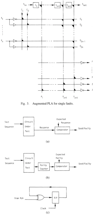
Ill. REMARKS A New PLADesignfor UniversalTestability
Theaugmentationneeded for the PLA is minimal: ashiftregister HIDEO FUJIWARA with as many cellsas there areproductterms in the PLA, andone
extraoutput line. Furthermore, thereisnogatedelayinserted in the Abstract -A newdesign ofuniversally testable PLA's is presented in normaloperation pathof the PLA. Thetestpatterns and theircorre- which allmultiple faults can be detected by a universal test set whichis spondingoutput responses arefunction dependent. Therefore,this independent of the function being realized by the PLA. The proposed scheme isnotappropriate for built-intest. However,the testpatterns design has the following properties. 1) It can be tested with function- and their expected responses are very simply derivable from the independenttestpatterns; hence,notest pattern generation isrequired. personality matrix ofthePLA. Note that the testpatternsused are 2) Theamountof extra hardware issignificantly decreased comparedto eitherX(i) orX(i -
j),
with the shiftregistereitheratS(i)state or the previous designs of universally testable PLA's. 3) Very high fault at the all-I state. The expected output patterns are either direct coverageisachieved, i.e.,allsingle and multiple stuck faults,crosspoint mapping of theORplane (inthe case of PROCEDURETHREE), or are faults,andadjacentlinebridging faults are detected. 4) It isappropriate determined by knowing whether a given input variable is "don't- for built-intesting approaches. 5)It canbe applied to the high-density care" foragiven productline. Thislatterinformationisagaineasily PLA'susing array folding techniques.derivable from the personality of thePLA in the AND plane.
The fault converage of this scheme is very high: all single and Index Terms-Built-in test, design for testability, fault detection, multiple stuck-at faults, crosspoint faults, and all combinations function-independent test, PLA folding, programmable logic array thereof are detected. The proof of the coverage is given in [6]. (PLA), testing, universal test.
Finally, the augmentation described here can be applied to folded
PLA's [3], [4], and [9]. For more details, see [6]. Manuscript received February 11, 1983; revised September 30, 1983. Table V shows the test patterns for the PLA of Fig. 1, assuming The author is with the Department of Electronic Engineering, Osaka Univer- that the PLA is augmented as shown in Fig. 2. For a PLA with n sity, Osaka 565, Japan.
0018-9340/84/0800-0745$01.00 C) 1984 IEEE
I. INTRODUCTION patterns and output test responses are both function independent under
single-fault assumption.
Because of the rapidly increasing circuit density in LSI/VLSI 5) The design can be applied to the
high-density
PLA's using technology, the testing problem is getting much more difficult and array folding techniques.worse.One approach to alleviate this problem is embodied in design fortestability techniques [ A].Withthesetechniques, sufficient extra
circuitry is addedtoacircuitorchip so as to reduce the complexity ll. AUGMENTED
PLA'S
FORMULTIPLE FAULTSof testingorthe cost of testing. The complexity or cost of testing can A PLA consists of three main sections: the decoder, the AND beclassified intotwocategories: one is the ease of test generation array, and the OR array. The decoder sectionusually consists ofa and the other is the ease of test application. For the first category, collection ofone-inputdecodersortwo-inputdecoders. A PLAcan theoptimumdesigntominimize the test generation cost is achieved beimplemented both in bipolar and MOStechnology. In thiscorre- by eliminating the expensive stage of test generation. Such a design spondence, we assume that the PLA's areNOR-NORimplemented in canbe accomplished by universal testing or function-independent NMOS technology and consist ofone-input decoders. These as- testing such that test patterns are predetermined independently sumptions do not affect ourargument. The results givenhere can of thefunction being realized. Various designs for universal testa- easily be modified to be applicable to PLA's implemented in other bility have been reported successfully for the circuits with regular technology, or withtwo or moreinput decoders. A PLA consists of structures such as Reed-Muller canonic circuits [2], [3] and pro- n inputs, 2n rows in AND array, m columns (product lines), and grammable logic arrays (PLA's) [4]-[7]. The PLA, which is con- erows(outputs) inOR array.
ceptuallyatwo-level AND-OR, is especially attractive in LSI/VLSI Consider theaugmented PLA shown inFig. 1.Itisaugmented by due to its memory-like array structure, and has become a popular adding a shiftregister, two columns between the decoder and the andeffectivetool forimplementing logic functions
[12]-[16].
AND array, and one column and one row to AND and OR arrays, The first contributions to the design of universally testable PLA's respectively. The extra connections shown in Fig. 2 are for an areFujiwaraetal. [4], [5] and Hong and Ostapko [6]. They have implementation in NMOS technology. The augrnented PLA can independently proposed'designsof PLA's which can be tested easily be obtainedbyexcluding twoEXCLUSIVE ORcascades from the PLA by function-independent test patterns. Although the designs of of Fujiwara[4],
[5:1, although the connections of the added Fujiwara [4], [5] and Hong [6] differ in implementation, the essen- column/row in the AND/OR array are different. Therefore, the tial idea is almost thesame.They both have extra circuitry to select amount ofextra hardware is significantly decreased compared to onerow line Of-AND array, a shift register to select one product line, theprevious designs of universally testable PLA's[41-[7].
and twoEXCLUSIVEOR cascades or trees to check the parity of the A shiftregister is added to select a column (product line) in the rowand column in the array. While these designs have succeeded in AND array. Each column Pi is ANDed by the complement of each reducing the costoftest generation, there still remain some prob- variableSi of the shiftregister as follows:lems. Both designsusetwo EXCLUSIVE OR cascades or trees which
occupyalargeextra areaof thechipinmosttechnology. Moreover, P, = p Si for i = 1, 2, , m only single faults for stuck and crosspoint faults are considered
in these designs
[4]-[6],
although most of the multiple faults arewhererpa
is a product term generated by the ith column of the originalalso detected. AND array. An extra product line Pm l is added which has devices on
Inorder to solve these problems of hardware cost and limited fault all crosspoints in the AND array, i.e., coverage,Salujaetal. [7]presented a design of PLA's with univer-
sal tests. The design of Saluja [7] notably excludes the two PI,+ Q Q2.Q2nl SmII+
EXCLUSIVE ORcascadesortreesthat existed in the previousdesigns, whereQ, is the ith row of the AND array. Anextra output line Z is andhas auniversal test setwhich detects multiple stuck and cross-
added
which has deviceson all product lines, i.e.,point
faults.However,
thedesignofSaluja[7]stillhasthe followingdrawbacks. Although it decreases the amount of extra hardware by Z=
_p
+p&
+ +pm
+ p, excludingEXCLUSIVE OR cascades or trees, the reduction is not suf-ficient since another shift register is appended.. , . Also,nthecircuitry to
.~~~~~~~~t
Twoextracontrol lines Cl andC2are addedtodisable allXi's
and select one row line of the AND array adds two gate delays to theXs, respectively,
as follows:normaloperationof the PLA; that is, the
speed
degradation is worsethan thePLA'sof
Fujiwara
[4], [5] and Hong[6]. Furthermore, fault -Xi
coverage is not complete since the bridging faults, which are im- = Cportant in PLA's, are not considered. Although the input test pat-
Q2i
=Xi
C2 for i = 1, 2, n terns are function independent, the output test responses in thedesign ofSaluja
[7]
are not function independent. This makes its whereXi is the ith input line andQj
is the jth row of the AND array. incorporation with built-in testing difficult. The section composed of 2 x 2n crosspoints on two control lines isInthiscorrespondence, a new design of universally testable PLA's called the control array of the augmented PLA. ispresented. The proposed design has the following properties. The augmented PLA has the following properties.
1) It canbetested with function-independent test patterns. For 1) The shift register can be used to select an arbitrary column of the design ofPLA's under the single-fault assumption, both the the AND array by setting 0 to the selected column and 1 to all other inputtestpatterns and output test responses are function indepen- columns. Note that since NOR logic is assumed, to select a column dent. However, under multiple-fault assumption the output test re- or product line
Pi,
Si should be 0 and all otherSi's
should be 1. sponses are not function independent. 2) The control array can be used to select any row of the AND2) The amount of extra hardware is significantly decreased com- array, i.e., to sensitize any output line of the decoder. To select pared to the previous designs of universally testable PLA' s [4]-[7]. Q2i- set XitoO0, all other X1' s to 1, C1 toO0, and C2 to 1I. To select The ratio of additional hardware to original hardware can be reason-
Q2i,
setX, to 1, all otherXj's to 0, Cl to 1, and C2 to 0. Note that ably small for LSI and VLSI chips. For example, for a PLA with inNOR logic selecting a row is equivalent to setting the row to 1 and 60 inputs, 60 outputs, and 200 product terms, the ratio is less than all other rows to 0.5 percent. 3) The extra column Pm±i inthe AND array can be used to test
3) Very high fault coverage is achieved, i.e., any combination of stuck, crosspoint, and bridging faults in the decoder and the control stuck faults, crosspoint faults, and adjacent line bridging faults in array, and also to test stuck and bridging faults on the rows of the
the PLA are detected. AND array.
4) It isappropriate for built-in testing approaches since input test 4) The extra row and output line Z of the OR array can be used
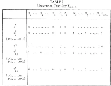
sin.
5;m tv
UNIVERSAL TEST SETTABLE IT,
X14.... ... X 1 S ... S S
==1 n 1 2 1 ... . m+1
L -- I 0 . 0 1 0 3. .
+_II2 ... .1 0 1 ... 0 ... 1
xn~~~~~~~~~~~~~~~~~~~~~~~~~~I
i ~~~~j=1,...,m+l1)
n_>0 2n-1 3
...1 0 1 1 ...10
kL
Pmn 4mi
TbeIFig.t.nAugmented PLA for multiplefaultsByTheoremI. 1, th... 0. 1 0 1 1.. 0 sm1s
(i.
F~
F
tet sIe0f... 1t... 0 10 1 .0 ....faults, and
bridging
faults inthe PLA,by
the test setTn,mep
shownPi
P~~M
Pm+l in TableI.
Fig. 1. AugmentedPLAformultiplefaults.
By
TheoremI,
thetest setT~,m+ is showntobethemultiple
fault test set for theaugmented
PLA's ofFig.
1. Furthermore, the test patternsofTn,,
m+ arefunctionindependent,
but theirresponses are notfunctionindependent. However,
the responses oftestpatterns
1 2 P. can be
easily
derivedfrom thepersonality
matrix of the PLA.UsingthetestsetTn,
±,
we canconstruct a test sequence for theSl Iaugmented
PLA's as follows:XjDT ); Q~~~~~2i-1vv
| _ | - ~L> ~ T,;~, ,~ ~ ~ Tn m+S I= |IJ21211112...Inl+I 2+II3I41 I41112 .ll.I/41n .. J4...I4nI ..J4Inm+I
Q2i
~ ~
I 11121
nfl
1J11ni+ I...nmi+
The lengthof the test sequence is 2nm + 2n + m + 3.
(a) (b) Finally, we will estimate the area of increase in the augmented
PLA's ofFig. 4. Let
AI
be an area of a transistor, let A2 be an area Fig. 2. Extra device in NMOS technology. ofapull-up, and letA3 bean areaofacell ofa shiftregister. Thenthe ratio ofextra hardwareto original hardware is
to teststuck andbridgingfaultsonthe columnsorproductlines and 0 = A(6n + m + e +1) + A3(m +1) x 100 crosspoint faults in the AND array in cooperation with other extra (A, + A2)(3n + t) + A,(2n + f)m + A2(r + f)
hardware.
(percent)
The types of faults considered in this section are the multiple
faults such that any combination of the followingtypes offaults Assumingthat A = A2 and A3 6 x A1, we have occurs simultaneously.
1) Stuck faults in the augmented PLA, i.e., stuck-at-0/1 faults - 6n + 7m + ( + 7 x 100 (percet) onthelines,
XK's,
Ci's, Qi's, P,'s, F1's,Z, andS1's. 6n + 2nm + (3m + m +3p2) Crosspointfaults in the controlarray, the ANDarray, and the
ORarray. Acrosspointfault is an extra oramissing device faultat In someof themore recent VLSIchips,PLA's take alargepart of thecorresponding crosspoint. thechips. Forexample, the BELLMAC-32A, a 32 bit single chip 3) Adjacent line bridging faults in the control array, the AND microprocessor [16], has eight PLA's. The sizes of these PLA's array,and the ORarray, i.e., bridgingfaults between C1 andC2, Qi range from 25 inputs, 12 outputs, and 42 product terms to andQi+, Pi and
Pi+1,
Fi and Fi+, andFe and Z. Thetechnology 50 inputs,67 outputs, and 190 productterms as shown in Table II. used, will determine what effect the bridging will have. In this Table I1 shows the ratio of hardware increase for the BELLMAC- correspondence,thePLA is assumedtobeNOR-NORimplementedin 32A ifwe redesign the eight PLA's with the universally testable NMOStechnology. Hence, abridgingfaultbetweentwo linescan PLA's ofFig. 1. The ratio is very small, and forlarger PLA's the be assumedtoproduce an ANDfunction betweenthe lines sincelow increase will become much smaller For example, for aPLA with will dominate in NMOS technology. However, the results given 60 inputs, 60 outputs, and 200 product terms, the ratio is less than here can easily be modified to OR-type bridging faults. 5 percent.Table I shows the test set Tn,m+i to detect all multiple faults
mentioned above, where n and m are the numbers of inputs and III. AUGMENTEDPL.A'SFOR SINGLE FAULTS
product lines, respectively, in the original PLA before augmen- InSection It, we have presented a design of universally testable tation. We can show thatTn,m+ is the multiple fault'testset for the PLA' s formultiple faults. The test setT1, m"+ ofFig. 1 is universal PLA's of Fig. 1 in the following theorem. The proof is omitted due since the testpatterns are independent of the function implemented tolimitation of space. For the detailed proof, see [20]. by the PLA, but their responses are not function independent. Theorem 1: The augmented PLA of Fig. 1 can be tested for all However, if we assume the single fault model, we can design an multiple faults, i.e., any combination of stuck faults, crosspoint augmented PLA for which both the input test patterns and their
TABLE
IIs
RATIOOFAUGMENTATIONFORBELLMAC-32A in 2outVW+1
I 2 PLA Inpu:ts Outputs Product Terms Ratio of Tncrease (% )
xl 8
1 50 67 1]90 5.3
2 30 27 120 9.7
3 27 514 1,81 74.
4 56 6i 136 5.7
5 30 37 153 8.5 n 2n-1
6 21'i 13 66L 16.2
7 -12 21 58 18.1
8 25 12 42 16.3
>°F1
Total 7.5 ,
responses are independent of thefunction. Inthis section, we will
present the PLAdesignunder single faultassumption. Z
The PLA'sforsinglefaultscanbesimilarly augmentedas shown L k L Z
inFig. 3. On thewhole,thestructureofaugmentedPLA is thesame
as that of Fig. 1, except the connections of devices on the extra pp++ p+2
columns androwsin theANDand theORarrays. TheaugmentedPLA
ofFig. 3hastwo extracolumns in theANDarray andtwo extrarows Fig. 3. AugmentedPLA forsinglefaults. in theORarray which satisfythe following conditions.
1) An extraproduct line Pm+2 is added which has deviceson all crosspoints in the ANDarray, i.e.,
Expec ted
Prn--2 = Ql Q2 Q2u Smnr2 Test Circuit Response
Sequence Under ResponseGodFut
where
Qi
is the ithrow of theAND array.Tes
Comparutor2) Anextra product line
Pn±i,
is addedwhich has devices at the twocrosspointsofQ,
andQ2, sothatPn+1 isalwaysset to0during
normaloperation of the PLA. (a)
3) The existence ofadevice atthecrosspointof
Pm±,
andQ3
is arrangedsothat the totalnumber of absence of devicesatthecross-points of P, and
Q2i--
for alli = I, ,n andj 1l, ,m + 1tEpetted
is odd. Test Circui't Parity
4) Similarly, the existence of a device at the crosspoint of '
P,,,
and Q4 is arranged so that the total number of absence of Sequence Under n±1Pi Purityt~~~~~~~~~~~~~~~~~~~~~~~~~~~~~~~~~~~--omparator Good/Faulty devices atthecrosspoints
ofPj
andQ2i
for all i = I, , n, and Test Counterj =1, ,m +l is odd.
5) An extraoutput lineZ,isaddedwhichhas devicesonalternate (b) crosspointsin the ORarray.
6) An extra output line Z2 is added which has devices on all crosspointsinthe ORarray.
7) The column
Pm+2
has deviceson alternate crosspoints in theORarray. F/F
8) For eachrowFiintheORarray, the existence ofadeviceatthe Pros
PLA
crosspointofPm+landFiis arrangedsothatthe number of presenceofdevices onthe crosspoints of PI, P2, P,m+I is odd. Clock
Thetypes of faults consideredinthis sectionarethesinglefaults (c) asfollows.
1) Single stuck faults in the augmented PLA, i.e., stuck-at-O/l Fig. 4. Testingschemes. (a) Conventionaltestingscheme. (b) Parity faultsonthe lines,
Xi's, Ci's, Qi's, Pi's, ZI,
Z2, andSi's.
compressiontestingscheme. (c) Paritycounter.2) Singlecrosspointfaults in the control array, theANDarray,and
theor array. We can show that Tn.m+2 detects all single faults in the PLA's of
3) Single bridging faults between adjacent lines in the control Fig. 3 in the following theorem.
array, the AND array, and the OR array. In the ordinary testing scheme, a sequence of test patterns is The test sequence to detect all single faultsmentioned above ts applied to the circuit under test and the response of the circuit is the same as that described in Section II. It is constructed by the
testsetT,,rn+asfollws,whee nandm ar th nuber of compared
against
thepreviously obtained
correct response one byipteste
inpus ad poduttrmsof he rlgial LA efoe agmetatOnSand prouc termflofs theoriginald
PLbefre ah ugmbentatin
one as shown in Fig. 4(a). In this section, we consider a differenttesting scheme using parity counters as shown inFig. 4(b).
The respectively,~~~~~~~~~response iS
compressed by a parity counter and then comparedn,n2= I1 I212,
*,2+ 213'1']l/2
1 .....q
4I4,m+ 2. '''In,m1+
2 against areferencevalue only at a predetermined time. The timing of paritycheckingand the expected parity of the responseforthe test 1111I21*.
*I51*.
* *IJ* *I1 m+2***In.
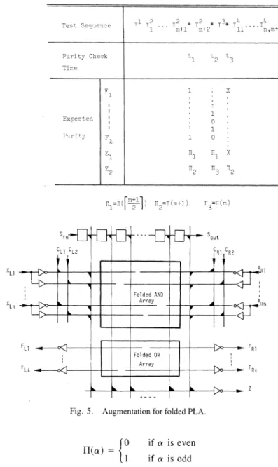
m+2. sequence Tn m+2are shown in Table III, whereTABLE III UNIVERSAL TEST SEQUENCE
. I I I 1* T2. T I I T
Test SequIence 1 T2 2 T* T **IT T
TsM+1M+to+2 I1 nn,+l t,a+2 mn,m+2 Il---n,ml,rn+2*
ParityParityCheckClDleck
~~~~
- tt~~2
3 4 t5 t6 t7 t8 t9Titre
"1 1 .X X X X X X X
xulec4e
10e,.0r.+7J7A 1 10
Z7 II P X X X X X X X
2 113 2 3 3 3 2 2 2
a 2 3=3l33.22)32 2
S;
n4{l#{E}T {SOUt
ACKNOWLEDGMENTc-4D
outcThe
author would liketothank Prof. H. Ozaki of Osaka Univer-CL1 CL2 C RF sity and
Prof.
K.Kinoshita
of Hiroshima University for theirx___,__
x 1 encouragement and support of this work. The author would alsoLl L- -
lllR1
like tothank Prof.
K. K. Salujaof the University of
Newcastle_ . KV_ ___, _ e and Prof. D. K. Pradhan of Oakland University for their helpful
FoldedAND
X L Array discussions.
xLn _2n___r_o0R,
L
~~~~~~~~~~~~~~~REFERENCES[1]
T. W. Williams and K. P. Parker,"Design
fortestability-A survey,"
FL _ ,l l l |Folded OR l_ _ FRl [2] IEEE Trans. Comput., vol. C-31, pp. 2-15, Jan. 1982.
S.
M. Reddy, "Easily testable realizations for logic functions," IEEEFL2<
_ _
ArrayF0_ t
Trans. Comput., vol. C-21,pp. 1183-1188, Nov. 1972.[3] K. K.Saluja and S. M. Reddy, "Fault detecting test sets for Reed-Muller _L L i > z s > _ Zcanonic networks," IEEE Trans. Comput., vol. C-24, pp. 995-998,
I- - - Oct. 1975.
[4] H. Fujiwara, K. Kinoshita, and H. Ozaki, "Universal test sets for pro-
Fig.
5.Augmentation
forfoldedPLA.grammable.logic arrays,'
in Dig. 10th nt.Symp.Fault-Tolerant
Com-puting(FTCS-10), Oct. 1980, pp. 137-142.
[5] H.Fujiwaraand K.Kinoshita, "A design of programmable logic arrays
floa
ifais even withuniversal tests," IEEE Trans. Comput., vol. C-30, pp. 823-828,01 if oeoddis Nov. 1981; also IEEE Trans. Circuits Syst., vol. CAS-28,
pp. 1027-1032, Nov. 1981.
and Fp1 is the smallest integer greater than or equal to 3, andX [6]
S.
J. Hong and D. L. Ostapko, "FITPLA: A programmable logic array formeans
notcecateimfunction-independent testing,"
inDig. 10th
Int.Symp.
Fault-Tolerantmeans not tocheckat the time. Computing
(FTCS-10),
Oct. 1980, pp. 131-136.Theorem2: The augmented PLA ofFig. 3 canbe tested for all [7] K. K. Saluja, K. Kinoshita, and H.
Fujiwara,
"Amultiple
fault testablesingle stuck faults, crosspoint faults, and bridging faults in the design of programmable logic arrays," in Dig. 11thtnt. Symp. Fault- PLA by applying test sequence
Tnm±+2
and comparing the com- Tolerant Computing (FTCS-11), June 1981, pp. 44-46.pressed parity of the response against the reference values at the [8] D. K.PradhanandK. Son,"The effect of untestable faults inPLAs,"in predeterminedtime as shown in Table III. Proc. IEEE TestConf., Nov. 1980,pp. 359-367.
The test sequence
'rn,,m±2
and its parity sequence shown in [9] K. Son and D. K. Pradhan, "Design ofprogrammable logicarrays for TableIII are both function independent. Moreover, the length of testability," in Proc. IEEE Test Conf., Nov. 1980, pp. 163-166.thepaeis9, and hence, the cost of storing the correct [10] S. Yajima and T. Aramaki,
"Autonomously
testable programmable logictesparseitw.
sequence arrays,"inDig. 1lthInt. Symp. Fault-TolerantComputing (FTCS-11), response iS very low. Hnetest sequencelud,md2
can be easily gener- June 1981, pp. 41-43.atedby ashiftregister. Hence, it is concluded that the PLA design [11] K. S. Ramanatha, "A design for complete testability of programmable of Fig. 3 and the testing scheme of Fig. 4(b) are suitable to logic arrays," in Proc. IEEE Test Conf., Nov. 1982, pp. 67-73. built-in testing. [12] H. Fleisher and L. I. Maissel, "An introduction to array logic," IBM J.
Res. Develop., vol. 19, pp. 98-109, Mar. 1975.
IV. CONCLUSIONS [13] C.Mead and L. Conway, Introduction to VLSI Systems. Reading, MA: The new design of universally testable PLA's presented in this Addison-Wesley, 1980.
paper has the following merits. 1) It can be tested with function- [14] R. A. Wood, "A high density programmable logic array chip," IEEE independent test patterns. 2) The amount of extra hardware Trn.Cmu,vo.-2,p.6-08Set19.
r 1 .1 . . . r
~~~~~~~~[15] G.
D. Hachtel, A. R. Newton, andA. L.Sangiovanni-Vincentelli,
"Anis~~~~~~~~~~~~ sinfcnl,erae
oprd otepeiu ein funalgorithm
foroptimal
PLAfolding,"
IEEE Trans.Comput.-Aided
De-versally testable PLA's. 3) Very high fault coverage iS achieved, sign, vol. CAD-i, pp. 63-77, Apr. 1982.
4) It is suitable to built-in testing. 5) It can be applied to the high [16] H. -F. S. Law
anld
M. Shoji, "PLA design for the BELLMAC-32A micro- density PLA's using folding techniques. Fig. 5Sshowsan augmented processor," in Proc. tnt. Conf. Circuits Comput., Sept. 1982,folded PLA for multiple faults. pp. 161-164.
[17] D. L. Ostapko and S. J. Hong, "Fault analysis and test generation for function determined by C. Equivalently, ift is irredundant, then programmable logic arrays," IEEE Trans. Coinput., vol. C-28, there exist appropriate tests that will detect each of the two faults: f pp. 617-626, Sept. 1979.
s-a-0 (stuck-at-0)
andfs-a-I
(stuck-at-l). A circuit C will be said[18]
J. E. Smith, "Detection of faults in programmable logic arrays," IEEE to be irredundant if every lead in C isirredundant. Given an irre- Trans. Comput., vol. C-28, pp. 845-853, Nov. 1979. ,, dundant combinational circuit C and a subset L of the leads inC,
[191 V. K. Agarwal,"Multiplefault detection in programmable logicarrays," i d ma tIEEETran. Coput, vo. C-9, p. 58-52, Jue 190 ' S (C)
iS defined
as themlni'mum
number oftestsrequired
todetect IEEE Trans. Comput., vol. C-29, pp. 518-522, June 1980.al[20] H.Fujiwara, "A new PLA design for universal testability," IECEJapan, all single stuck-at faults on the leads in L. If L is the set of all leads Monog. EC83-2, Apr. 1983, pp. 11-22. in C, then we denote SL(C) by S*(C). We will investigatethefollow-
ingthree problems associated with estimating SL(C) and S*(C). 1) Generalized Minimum Test Size (GMTS) Problem: Given an irredundantcircuit C and any subset L of the leads in C, compute SL(C).
On theComplexityofEstimating the Size ofaTest Set 2) Minimum Test Size (MTS)
Problem:
Given an irredundant BALAKRISHNAN KRISHNAMURTHY AND circuit C, computeS*(C).SHELDONB. AKERS 3)
a-Approximate Minimum
Test Size (AMTS(a)) Problem:Given an irredundant circuit C anda > 1,compute a numbertsuch Abstract-Most NP-completenessresults for testgeneration problems that S*(C) . t ha
Sar(C).
involve a reduction to theredundancy problem,whichexplicitlv encodes It will be shown that all of these problems are NP-hard. We do this the satisfiability problem. In this correspondence we investigate the by showing that the satisfiability (SAT) problem is polynomially complexity of a more modest problem -that of estimating the size of atest reducible to each of the above problems. To this end, we begin setunder the constraint that the circuitis irredundant. We show that even with a Boolean formula F and construct a circuit for which the thisconstrainedproblemisNP-hard in thestrong sense. corresponding answers will enable us to quickly determine ifF
issatisfiable.
Index Terms -Combinational circuits, complexity, redundancy, test- First, we constructa circuitC1(F) from aBoolean formulaF as
ability, testsets. shown inFig. 1. Without loss of generality, it is assumed that Fis
expressedin aproduct-of-sums form withnvariables and ktermsin INTRODUCTION theproduct.Wenotethat the circuit realizes the formula F, i.e., for The recent trend towards the incorporation of testability into any given input, the output of the circuit will be the value ofthe digital design procedures has placed renewed emphasis on the need formula. InFig. 1, the variablesofF arerepresentedasv,, v, , forquantifying thistermprecisely. This,inturn,hasledresearchers v,,. Thereis an OR-gateGiforeach of the ktermsin theproduct. The toconsider thecloselyrelatedproblemofdetermining thesizeofthe inputs to each such gate are either the variables
vj
or their com- test set necessary to detect a specific set of faults within a given plements. Theseinputswillbereferredtoasliteralstoindicate thatdigital circuit. theyare variables with possibly complementation. We canassume
For specialized circuits and functions, a number of results have that none ofthe G, gates contains both literals of a single variable. already been obtained. These relatetofan-out-freecircuits [7], unate Thus,each Gihas at most n inputs.
functions[2],linear circuits[4], AND-ORcircuits [ 1], etc. However, Aprimary input isan inputto agate in the circuit that is notan the extension of these results to more generalized circuits (even outputofanyother gate inthecircuit. Forexample, all inputsto the purely combinational ones) has thus far been largely unsuccessful. GgatesinCl (F)areprimary inputs, whereastheinputstothe Agate On the otherhand, the well-knownresultsby Ibaraki et al. [8], are notprimaryinputs. Clearly, aprimary input canalways be set Ibarra and Sahni
[9],
and others show that a number of testgen- to any desired logical value. In addition, we make two simple eration problems belong to the class ofnotoriously difficult NP- observations onC,(F)that willbe usedrepeatedlyin thesubsequent complete problems [6]. Thus, we areessentially asking ifwe can arguments.easily estimate the size ofaset eventhough the actual determination 1) The output of any oneG-gatecanbeset to anydesired logical of thesetitself may bequitedifficult. However,evenhere, all may valueby appropriately setting the primary inputs tothatgate. not be lost. Polya's famous counting theorem [3], for example, 2) The outputs of all the G-gates can be simultaneously set to shows that it is often possible to calculate the exact size ofasetof 1 iff the formula F is satisfiable.
classeseven thoughwemay haveno simple wayofactually deter- C,(F)is the firstof the circuits that we will construct in thispaper. mining arepresentative of each class. Observe that CI(F) may not be irredundant. In fact, a s-a-0 fault In what follows, three problems relatingto test size estimation can be detected onoutput lead
0
iff F is satisfiable. This follows willbe formally stated. Proofs will then be given that all threeof immediatelyfromobservation 2andthusproves that the redundant these problemsare NP-hard. lead problem is NP-hard-a result already shown in [9]. In the remainder of thiscorrespondence, we construct irredundant circuits fromarbitrary Boolean formulas and use them to prove that SAT is PRELIMINARIES polynomially reducible to the three problems mentioned above. We Inthiscorrespondencewewill beconcerned with theproblemof denote polynomial reducibility byxa
estimatingthesizeofatestsettodetectallsinglestuck-at faults in
an irredundant combinational circuit. Specifically, let C be a MAINRESULTS combinational circuit. A lead t in C is said to be irredundant
wheneverreplacingf by aconstant logicalvalue (0 or 1) changes the We
begin
byremoving
the redundancy inC,(F). To do this, we constructC2(F) as shownin Fig. 2. The k additional primary input leads are w,, w2, , Wk. Nowthe first lemmafollows.Lemma 1. Forany Boolean formula F, C2(F) is irredundant. Manuscript received March 18, 1983; revised November 18, 1983. This Proof: To show that all leads of C2(F) are irredundant, it will work was supported by the U.S. Air Force, AFSC Aeronautical Systems sufc to sho tha an rirr rmr nu edcnb Division, under Contract F336- 15-80-C- 1083. sensictizd-o .valueshacanyaberassine tothey othlerdvaranbleso
B. Krishnlamurthy is with the General Electric Research and Development seitzd ..,vlscabesigdtoheteraibeso Center, Schenectady, NY 12301. that the value on this lead will appear at +6.
S. B.Akers is with Military Electronic Systems Operation, General Electric Consider the first input lead to gate G1 with input value a,. To Company, Syracuse, NY 13221. make 4 sensitive toa,, we set the other inputs to G1 toO0, as well as