An Energy-Efficient ECC Processor of UHF RFID
Tag for Banknote Anti-Counterfeiting
XI TAN1, MIANXIONG DONG2, CHENG WU1, KAORU OTA2, JUNYU WANG1, AND DANIEL W. ENGELS3, (Senior Member, IEEE)
1State Key Laboratory of ASIC and System, Fudan University, Shanghai 200433, China
2Department of Information and Electronic Engineering, Muroran Institute of Technology, Muroran 050-8585, Japan 3Computer Science and Engineering Department, Southern Methodist University, Dallas, TX 75275-0100, USA
Corresponding author: K. Ota ([email protected])
This work was supported in part by the National Science and Technology Pillar Program of China under Grant 2015BAK36B01, in part by the National Natural Science Foundation of China under Grant 61076022 and Grant 61211140046, in part by the Shanghai Pujiang Program, and in part by JSPS KAKENHI under Grant JP16K00117 and Grant JP15K15976.
ABSTRACT In this paper, we present the design and analysis of an energy-efficient 163-b elliptic curve cryptographic (ECC) processor suitable for passive ultrahigh frequency (UHF) radio frequency identifica-tion (RFID) tags that are usable for banknote authenticaidentifica-tion and anti-counterfeiting. Even partial public key cryptographic functionality has long been thought to consume too much power and to be too slow to be usable in passive UHF RFID systems. Utilizing a low-power design strategy with optimized register file management and an architecture based on the López–Dahab Algorithm, we designed a low-power ECC processor that is used with a modified ECC-DH authentication protocol. The ECC-DH authentication protocol is compatible with the ISO/IEC 18000-63 (’’Gen2’’) passive UHF RFID protocol. The ECC processor requires 12 145 gate equivalents. The ECC processor consumes 5.04 nJ/b at a frequency of 960 kHz when implemented in a 0.13-µm standard CMOS process. The tag identity authentication function requires 30 600 cycles to complete all scalar multiplication operations. This size, speed, and power of the ECC processor makes it practical to use within a passive UHF RFID tag and achieve up to 1500 banknote authentications per minute, which is sufficient for use in the fastest banknote counting machines.
INDEX TERMS Enter radio frequency identification, elliptic curve cryptographic algorithm, low power, authentication.
I. INTRODUCTION
This Ultra High Frequency (UHF) Radio Frequency Iden-tification (RFID) systems have made considerable progress since backscattering theory first appeared in 1948 [1]. The large, multi-component, high-energy devices that intention-ally generate a backscatter communication signal have been replaced by a single, ultra low-power microchip connected to a tuned antenna. The single microchip plus the antenna and packaging constitute a passive RFID tag that is capable of backscatter communication with an RFID reader. A passive RFID system consists of at least a tag, a reader and a data management system. One or more tags are attached to an object, and when that tagged object enters the communication zone of a reader, the modulated radio frequency (RF) signal transmitted by the reader is received by the tag. The tag harvests energy from the reader’s RF signal to power the microchip. The tag chip demodulates the RF signal, executes
functionality in response to the signal and backscatters a response according to the message in the signal. The reader sends all tag responses to the data management system where useful functionality is performed.
Low cost passive RFID systems are widely used in a broad, range of applications, such as logistics, retail sales, just-in-time manufacturing and electronic tolling, and they are being adopted for use in an ever growing number of new applications. In applications where personal, financial or critical data is communicated from the tag, the information transferred between the tag and the reader must be secured. Encrypted communications must be used to avoid private information leakage and severe economic and safety risks in these sensitive applications. Symmetric key encryption algorithms, such as AES (Advanced Encryption Standard), can be implemented on the low-power tag microchip within the size, power consumption and speed limitations typical of
passive RFID tags [2], [3]. Symmetric key algorithms require that both the reader and the tag share the same secret key; therefore, the use of symmetric key ciphers on tags used in large open systems presents a significant key management problem. In contrast, asymmetric ciphers, such as ECC (Ellip-tic Curve Cryptography), provide for simple key management by allowing for the public key for a tag to be widely and easily distributed while requiring only that the secret private key be stored and used only on the tag itself.
We note that the ECC enabled RFID tag can be used as an anti-counterfeit mechanism for an item that works in addition to the traditional physical anti-counterfeit mechanisms. The use of a unique private key on every tag makes it difficult for a counterfeiter to obtain a sufficiently large number of private keys to make counterfeit products, such as counterfeit bank notes, that are difficult to detect due to the reuse of the compromised private key. And, with sufficient physical protection of the memory storing the private key and the functions using the private key, it is prohibitively expensive for all but the most well funded attackers to retrieve a private key from a single RFID tag chip.
In this paper, we present the design of a low power (5.04 nJ/bit) ECC processor for a passive UHF RFID tag that is suitable for use in banknote authentication. Among the various secure asymmetric algorithms, ECC is the most usable for passive RFID systems due to its small key size. The smallest NIST (National Institute of Standards and Tech-nology) recommended key size is only 163 bits [5]. Juel and Pappu [6] were the first to propose a practical RFID banknote authentication scheme which was later modified by Yanget al.[7] to overcome various attacks. These schemes utilize an asymmetric algorithm to provide security. However, neither Juels and Pappu nor Yang et al. select a specific asymmetric algorithm for use. Consequently, neither provides a potential hardware design or implementation evaluation to evaluate the feasibility of their schemes. Tuyls and Batina present a basic ECC processor architecture for use with PUFs (Physically Unclonable Functions). However, Tuyls and Batina did not implement or synthesize their architec-ture; therefore, their size and power calculations are only estimates. Furthermore, none of these works were designed to work within the most common passive UHF RFID protocol, the EPC Gen2 air interface protocol [9]. Our ECC processor design works with a modified ECC-DH authentication pro-tocol that is compatible with the most recent EPC Gen2 air interface protocol, EPC Gen2v2.
The remainder of this paper is organized as follows. Section II presents and analyzes the design requirements for RFID enabled banknote authentication. We summarize previously published ECC implementations in Section III, and we summarize the relevant portions of the EPC Gen2v2 protocol in Section IV. In Section V we review the ECC algo-rithm, present the tag microchip architecture and demonstrate how the modified ECC-DH protocol works within the EPC Gen2v2 protocol. Section VI presents the hardware realiza-tion of the ECC processor highlighting the optimizarealiza-tions of
the ALU (Arithmetic Logic Unit) including the multiplica-tion, squaring, modulo and addition operations and the key controlling module. In Section VII we present the simulation results of our ECC processor design through FPGA simula-tion and the synthesis results using 0.13µm CMOS process. We draw the relevant conclusions in Section VIII.
II. REQUIREMENT ANALYSIS
A passive UHF RFID tag is an ultra-low-power device that operates in the 860-960 MHz frequency range. A passive RFID tag harvests all of its operating energy from electro-magnetic waves incident upon its antenna and communicates through backscatter, a form of modulated reflection, com-munication. Passive UHF RFID systems provide for long communication ranges, up to 30 m today, between a reader and a simple identity only tag [10]. However, the required communication range for secure tags is typically significantly shorter with ECC-enabled banknote tags requiring only up to 20 cm communication range. With a communication fre-quency of 900 MHz, 20 cm is at the boundary of the near field and the far field. Since most banknote communications will occur at less than 20 cm, we utilize the near field model to analyze the power available to the tag. In general, the power received by the RFID tag chip can be expressed using Eq.1 with its components as defined in Eq.2 and Eq.3.
Pchip =PreaderρCτ (1)
ρ = 4RrRt |Zr+Zt|2
, τ = 4RcRa |Zc+Za|2
, C =GtLpathGrp
(2)
Lpath =(
λ
4πd) 2
(3)
For a reading distance of 20 cm at 900 MHz, we expect that a tag will have at least 1mW of incident power. This power level is easily achieved since the maximum radiated power for a reader is 1 W. However, given the potentially small reader and tag antenna that are likely to be used for banknotes, we take a conservative approach to the power requirement. A tag with chip sensitivity of 12 dBm (sensitivity between -18 dBm and -21 dBm is common today) will be able to harvest 63µW for its chip operations from 1 mW of incident power. A typical Gen2 tag requires approximately 10µW to operate without security [11]. Therefore, the security operations must consume less than 53µW of power.
Nowadays, the typical speed of banknote counting machines is between 900 and 1,000 notes per minute. Some specially designed machines work at speeds up 1,200 notes per minute. We set our design goal at a speed of 1,500 notes per minute to insure that even the fastest machines are accommodated by our design. This speed provides for 40ms for the complete communication between each tag and the reader.
ECC-DH needs only one ECC encryption operation (and no inversion operations) to be performed on the tag. Thus, the ECC encryption operation must take no more than 40 ms to complete as to allow for reasonable communications.
III. ECC RELATED WORK
Low-power and compact implementations of ECC processors have been explored well beyond the López-Dahab Algo-rithm. Optimized implementations have been proposed since at least the mid-1980’s [15], [16]. Interest in implementa-tions amenable to passive UHF RFID systems has arisen more recently. Lee et al. [17] propose a reduced register ECC processor that utilizes redundant modular operations to achieve performance usable with RFID systems. Using a 0.13 µm CMOS process, the synthesis shows that their design requires less than 12,500 Gate Equivalents (GEs) and consumes 12.08 µW. In [18], the first hardware implemen-tation of a binary Edwards curve is presented. The authors suggest the use of mixed ω-coordinates with the common
Z – coordinates to reduce the size of the register file. The design is realized in 13,427 GEs and takes 149.5 ms to finish computation when clocked at 400 Hz. Batina et al. [19] evaluate HECC and ECC over composite fields and reduce the register number to reduce gate count. Their results show the combination of two fields will reduce the size of the ALU module while the memory required will be slightly bigger. Kumar and Paar [20] present an area optimized ECC processor over a binary field. Inversion operations and fast square modules are implemented in the design with affine coordinates. An area between 10,000 and 18,000 GEs on a 0.35µm CMOS process is achieved. Hein et al. [21] present a fully functional ECC enabled RFID implementation that can fulfill the requirements of passive HF RFID tags com-patible with the ISO-18000-3-1air interface standard. The power consumption obtained by measurement is 8.57 µW at 106 kHz. Bock et al. [22] present a challenge response protocol similar to ECC-DH for tag authentication. Their 163-bit ECC engine is less than 0.8 mm2 in a 220 nm CMOS technology. The energy consumed is 79 µW at 847 kHz. Ting et al. [23] designed a very constrained device by imple-menting a scheduling of atomic operations. The architecture of the ALU and the use of a circular shift based register file realizes the scheduling effectively. By using 65 nm process, their design is implemented in 11,831 GEs and consumes 4.50µW with a clock frequency of 140 kHz.
These ECC related works utilize a range of methods amenable to passive RFID tags. However, each consumes either too much power, too much area or too much time to meet the requirements for banknote machines. The work presented in this paper focuses on designing a highly energy-efficient ECC processor suitable for banknote machines. Our presented design utilizes various low power design strate-gies to reduce power consumption at the expense of a slightly larger area. Additionally, our register file management is optimized for low power operation, and it has better perfor-mance than the shift register method proposed in the related
works. The execution time of the baseband integrated with our processor meets the requirement of the Gen2v2 protocol and the banknote machine.
IV. THE EPC GEN2 PROTOCOL
The EPC Gen2 air interface protocol standard was first pub-lished in 2004 [24]. It defines the physical and logical require-ments, including the Physical layer and the Link layer, for a passive UHF RFID system. The security enhanced version of Gen2, Gen2v2, was ratified in 2013 and was the first major update to the protocol since 2008.
The Gen2 protocol was designed for the field of retail supply chain. But in recent years, its use has been extended to applications including driver’s license and access con-trol [25]. The security and privacy requirements of these new applications led to the development of the Gen2v2 protocol.
The primary functionality of the Gen2 protocol involves the singulation and identification of tags within a reader’s communication zone. This identification process utilizes a framed slotted Aloha anti-collision protocol to first singulate a tag and then retrieve the unique identifier stored within the tag.
TABLE 1.Primary Gen2 identification commands.
The basic identification process utilizes four commands as defined in Table I. TheSelectandQuerycommands select a subset of the tags to participate in the identification pro-cess and then begin the identification propro-cess respectively. A tag, upon receiving theQuerycommand, randomly selects a slot number from within the range specified by the Query command. For everyQueryRep command received, the tag decrements its counter by 1. When a tag’s counter reaches zero, the tag communicates a 16-bit random number (RN16) to the reader. The reader, upon receiving an RN16, sends theACKcommand with the received RN16 as the command payload. The tag, upon receiving an ACK command with its just sent RN16, communicates its entire stored unique identifier to the reader.
When the tag communicates its identifier to the reader, the tag is singulated, meaning that only that tag is communicat-ing with the reader. From this point, the reader may issue commands directly to the tag with all other tags ignoring the sent commands. Once the reader has completed its com-munications, if any, with only the singulated tag, the reader issues aQueryRepcommand to move to the next slot in the identification process.
includes new security features and security functionalities including:
• Untraceable function to hide portions of memory.
• Cryptographic authentication of tags and readers to
reduce risk of counterfeiting and unauthorized tag access.
• Enhanced User Memory for supplementary encoding
and file access.
• Non removable flag to indicate that a tag has been
removed from its original packaging.
Authentication is the primary security function for Gen2v2 compliant tags. Tag authentication allows the reader or infor-mation system to authenticate the identity of the tag while reader authentication allows the tag to authenticate the reader prior to allowing access to the tag’s resources. Authenti-cation begins with the Authenticate command issued to a singulated tag. The first Authenticate command is used to authenticate the tag to the reader or information system. For banknote authentication, only tag authentication is required in an embedded tag.
The Gen2v2 protocol utilizes a new kind of function called
in-process reply. An in-process tag reply is a reply that meets T5 time restriction rather than the much more stringent T1 time restriction. The in-process reply allows the tag to indicate to the reader that it is continuing its execution of a command but is not yet completed. The in-process reply also allows the reader to be certain that the tag is still sin-gulated and powered. The T5 timing constraint for the in-process reply allows the tag to perform functions that require a relatively large amount of time (10’s of milliseconds). The in-process reply is usable with theAuthenticate command; therefore, it is possible to have cryptographic functions that take 10’s of milliseconds to compute. Therefore, the in-process reply of the Gen2v2 protocol greatly facilitates ECC processor design.
V. SYSTEM ARCHITECTURE
A. ECC ALGORITHM SECURITY ANALYSIS
Elliptic curves that are most amenable for passive UHF RFID systems are defined over GF(p) and GF(2n), wherep is a prime number and nis the order of the irreducible polyno-mial. Both fields have their own advantages when providing the same level of security based on the Elliptic Curve Dis-crete Logarithm Problem (ECDLP). TheGF(p)field enables simple squaring operations in ECC scalar multiplication by simply shifting the operand, while theGF(2n) field allows for a simple bit-XOR addition implementation. Due to the sim-ple CMOS circuit realization of bit-XOR,GF(2n) is usually chosen for low-cost designs.
The most important operation of ECC is elliptic curve scalar multiplication, i.e., kP = P+P+ · · · +P
| {z }
k times
, where
P is the 4 base point on the elliptic curve and k is the scalar operand. Scalar multiplication can be divided into sub-operations (point addition and point doubling) using the
Montgomery Ladder algorithm which prevents simple power analysis attacks [12]. The point operations are realized by finite field operations: addition, multiplication, squaring and division.
The López-Dahab Algorithm [14] is an optimized Mont-gomery algorithm that minimizes on-tag ECC function-ality and allows the tag to compute efficiently elliptic scalar multiplication in a hardware-restricted environment. The compute intensive operations are performed by the reader.
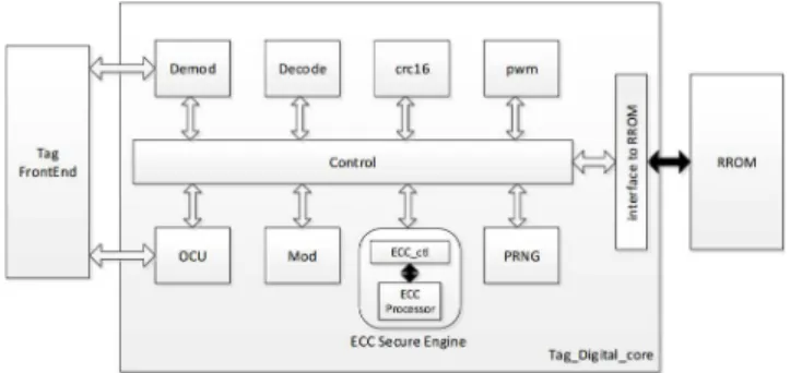
FIGURE 1. ECC tag microchip baseband architecture.
TABLE 2.Baseband module.
The method has two versions based on affine-coordinates (LD2A) and projective-coordinates (LD2P) respectively [13]. In this work, LD2P is adopted since algorithm LD2P is immune against timing attack. Because in [14], step 4 exe-cutes theM addandM doublein both cases of ki = 1 and ki = 0, the algorithm does not depend on theki value, it has no secret key dependency nor executing procedure of cryptographic transaction [13].
B. BASEBAND ARCHITECTURE
This ECC processor can be integrated into an RFID digi-tal baseband compliant with the Gen2v2 protocol shown in Fig.1.
message received is without transmission errors. Only error free messages are processed. The Decode module analyzes the message on the basis of EPC Gen2v2 protocol to get the command from the message. PWM is a power module con-sisting of several clocks set at different frequencies to meet various requirements of the tag modules. Reducing module frequency can reduce power consumption to a large extent. The PRNG, Secure Engine and RROM work together to deal with arithmetic computation and generate the tag response. The Mod module modulates the signal as an opposite process to Demod. At last, the final output is transferred back to the reader via the Tag Frontend and OCU.
C. ECC-DH PROTOCOL
Elliptic curve cryptography has been the basis of many cryp-tographic protocols for authentication and key agreement. The first protocol is due to Diffie and Hellmann [26], which is described in [27] as a key agreement method between two entities based onGF(p).
The ECC-DH protocol is described in [28] in detail. Some of its commands are selected to construct a simple version in this paper. This version consists of the basic functions necessary for tag authentication. The authentication process is illustrated in Fig.2.
FIGURE 2. Elliptic Curve static Diffie-Hellman authentication.
In the protocol, there are 3 commands: TAM 1.0, TAM 1.1, TAM 1.2. The tag has a static public/private key pair and a public key certificate. In a real application, the certificate should use a digital signature to bind the public key with the name of the organization that produced the key pair. During the certificate verification period, the reader should check whether the public key in the certificate is authentic by executing the signature verification algorithm. If the signature is invalid, the tag will not be accepted. In this version, we use an array of numbers to represent the certificate. The tag should give the right series of numbers back according to the reader’s command (TAM 1.1: Request Certificate). The reader has the authority to write a new certificate into the tag’s memory (TAM 1.0: Write the Certificate) if the tag is writable.
The detailed verification process (TAM 1.2) is displayed in Fig.3. TherG, qTandrQoperations are ECC scalar multi-plications. After the reader verifies that the tag’s certificate
FIGURE 3. ECC Verification Procedure (TAM 1.2).
is valid, it generates an ephemeral random number r and multiplies the base pointGwith this number. Then, the reader sends the temporary resultT to the tag. Upon receiving the challenge, the tag executesqT. The tag communicates the m resultqTxandqTzback to the reader. The reader calculates the projective coordinates(rQ)x (qT)z and(rQ)z (qT)x to check whether they are equal. If the response is correct, the reader accepts the tag.
In the whole communication process, the tag only needs to calculate one scalar multiplication and this operation is done in the projective coordinate without inversion or division. Therefore the computation overhead is quite low due to the short calculation time. In this design, we mainly focus on realizing TAM 1.1 and TAM 1.2.
VI. CIRCUIT IMPLEMENTATION
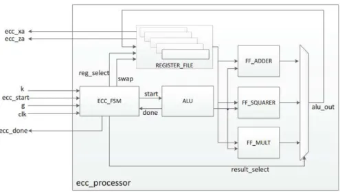
The system architecture is shown in Fig.4. The ECC proces-sor consists of 6 main modules described in the following. The ECC_FSM module controls the whole system according to a finite state machine. The REGISTER_FILE module has a 5∗163 bit register array that is controlled by reg_ select
andswap. The ALU module consists three finite field opera-tion modules: FF_ADDER, FF_SQUARER and FF_MULT, mapping to addition, squaring and multiplication operation respectively.
In Fig.4,krepresents the scalar key value; g refers to the x-coordinate of the base point in affine format received from the tag;ecc_startis the enable signal;ecc_xaandecc_zaare
xandzof the final output results sent back to the reader. Five 163-bit registers are used in the REGISTER_FILE module, and one intermediate register is used in the FF_MULT mod-ule in order to save chip area. The following sections explain the design of the modules in detail.
A. ALU
FIGURE 4. ECC processor system structure.
FIGURE 5. Multiplication hardware structure.
1) ADDITION
In this work, non-supersingular elliptic curve over finite field andGF(2163) is used as the base [29]. The elliptic curve can be represented by (4).
y2+xy=x3+mx+n (4m3+27n26=0) (4)
Assumingy=x163+x7+x6+1 to be irreducible polyno-mials.
ForP =P162i=0pixiandQ =P162i=0qixi, then R would be calculated by (5).
R=P+Q=
162
X
i=0
(pi+qi)xi = 162
X
i=0
rixi (5)
The calculation can be accomplished with exclusive-or (XOR) operation in hardware without carry transmission. The
delay only comes from the combinational circuits, which is acceptable for hardware implementation.
2) MULTIPLICATION
Multiplication operation is to calculate the result ofsk. The multiplication operation contains polynomial multiplication and modulo reduction [30].
sk =
X
i+j=k 0≤i,k≤m−1
ajbj, k=0,1,2, ...,2m−2 (6)
m−1
X
i=0 cixi =
2m−2
X
k=0
skxk modf(x) (7)
set to one or more and the computation sequence ofbcan be started from the Most Significant Bit (MSB) or from the Least Significant Bit (LSB). Furthermore, if the multiplication and the reduction are not finished together, extra register is needed to store the intermediate variables. For this reason, it is effi-cient to finish the multiplication and reduction in one clock round together. Another concern is how many bits should be used to do one round of multiplication. In the algorithm, in each round w bits are chosen from the key k to do partial multiplication, and then the followingwbits ofkare shifted out to calculate the next part. Too large w results in huge hardware cost, while too smallwleads to longer computation time. Taking area and efficiency into consideration [22] and in order to meet the strict requirement of completing 1,500 authentication in one minute, 5 bits are the suitable choice. The calculation sequence is MSB because this sequence can reduce the number of modulo reduction.
The structure is demonstrated in Fig.5. The input counter chooses w bits through the MUX, then multiplies it with A via network AND-XOR and XOR. The partial results are stored in a temporary register p and will be sent to AND-XOR network as an input for the next partial multiplication. A log2[m/w]-bit counter register adds 1 to itself after every clock in order to control the MUX by selecting w bits as an input. As a result, the multiplication operation consumes [m/w] clocks with the last result, indicated by signaldone, being stored in the register module. The whole multiplication takes 33 clocks to finish ifwequals 5.
3) SQUARING
The squaring operation means that operands A and B of the multiplication are equal. Though the reuse of the mul-tiplication module reduces hardware overhead, the squaring operation can be implemented much more efficiently, using fewer than 33 clock cycles, than the generic multiplication operation.
In order to optimize the multiplication circuit, first, let
P162
i=0cixi≡P162i=0aix2i≡P324i=0a ′ ixi, so
a′i=
(
ai
2, i=0,2,4, ...
0, i=1,3,5, ... (8)
Using the conversion above, we can deduce the equa-tion from the multiplicaequa-tion algorithm. The squaring module requires only 252 XOR gates with a critical path delay of 3Txwhere Tx is the XOR gate delay. The squaring module is a combinational logic circuit that can be executed in only one clock cycle. By this means, the performance of the ECC processor is improved with a minimal increase in area.
B. López-Dahab DATA FLOW
The López-Dahab computation data flow is shown in Fig.6. (X1, Y1) and (X2, Y2) are two sets of operands in projec-tion coordinates format for scalar multiplicaprojec-tion. The left side presents the point-doubling operation and the right side presents the point-addition operation. According to
FIGURE 6. López–Dahab algorithm computation process.
FIGURE 7. Data flow of ALU control module.
López- Dahab algorithm, the present bit of k determines whether (X1, Y1) and (X2, Y2) should be swapped. In Fig.6, no more than 5 variables are required to be stored at a specific time because addition and multiplication can be done by X1, X2 and Z1, Z2, T respectively. According to the modified ECC-DH protocol, only X1, Z1 need to be communicated back to the reader in the end.
C. CONTROL MODULE DESIGN
1) ALU CONTROL MODE
In Fig.6, only five registers are used to finish ECC scalar mul-tiplication. The register file is designed in the format shown in Fig.7. Assuming the data bus in ALU is m-bit width, five registers are connected to the inputs of ALU, and the stored value can be refreshed through ALU output. Certain signals control the moment to refresh registers. According to the López-Dahab algorithm, in every step, only one register’ will change the value while the others stay the same. So the ALU module selects which one or two operands in the register file should be used as the inputs for the operation procedure, then the ALU module calculates the result, places the result on the output wire via the MUX module, and tells the ECC_FSM module that the calculation is done. The ECC_FSM module asserts thereg_selectsignal to choose one register to replace the value with thealu_outoutput.
time, so the static power is low; the other is that the ALU module can easily choose which finite field operand will be used and where to find the operands. Compared with the Circular Shift File Architecture [17], our architecture makes it easier to control the data flow and consumes lower energy.
2) KEY CONTROL MODE
According to the López-Dahab algorithm,kdetermines the value put into the point-addition and the point-doubling mod-ule, andswapcontrols whether the register file will swap the value in the register array. Additionally, the counter is con-trolled byclkand is used to determine when the calculation process is finished. If the calculation is done,donewill be sent to the output.
D. POWER OPTIMIZATION
Power consumption is one of the most significant restrictions of passive UHF RFID tags. Power consumption consists of both dynamic power and static power with total power being the sum of these two.
Totalpower=DynamicPower+StaticPower (9)
Dynamic power is composed of switching power and inter-nal power. Switching power is caused by charging and dis-charging output load. Internal power is made up of short circuit and charging internal load. Static power is the power consumed when the circuit is in a stable state. For an ECC processor implemented in an RFID tag, power consumption optimization should be analyzed for both dynamic power optimization and static power optimization.
In addition to architectural power optimizations, traditional multi-clock domain technology and clock gating strategies are implemented [31], [32]. Multi-clock domain, in partic-ular, is applied in the PWM module in the baseband.
FIGURE 8. Clock gating structure.
The clock-gating structures are shown in Fig.8. The addi-tional combinaaddi-tional logic can avoid dynamic power. The clock gating technique is mainly applied to the register file. At every state, only one register will change the value with the ALU output, and the other four registers remain unchanged. The application of the clock-gating technique significantly reduces the power consumption of register files.
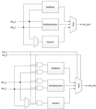
In this paper, operand isolation is also adopted to reduce the power consumption caused by invalid transitions. The ALU module is taken as an example here.
FIGURE 9. ALU structure.
Fig.9 shows the comparison between the original ALU version and the revised power efficient ALU version. In the original version, when values onaluin_1oraluin_2change, modules ADD, MULT and SQR will work at the same time, despite only one module’s result needing to be changed. In the power efficient version,sel_1andsel_2are set to different values to induce expected changes so as to avoid the other two modules’ operation. As a result, power consumption will be reduced.
VII. SYNTHESIS AND VERIFICATION
The ECC processor presented in this paper was synthesized using the Synopsys Design Compiler targeting a standard 0.13µm CMOS process. The power consumption estimation is generated with PTPX taking the node switching rate of the circuit into consideration rather than adopting the Design Compiler result. The synthesized ECC processor occupies an area of 0.3 mm×0.3 mm. The synthesis results of area and power are shown in Table III. In the synthesized circuit, thereg_file module takes up 48.4% of the area. The ALU (including the ALU, adder, squarer, and multiplication mod-ules) occupies 40.9% of the area, and thealu_in_muxmodule consumes 6.9% of the area.
TABLE 3. Synthesis area and power report.
has finished its computation, we gate the clock to the output register to clock only when the output is to be stored. As a result, even though the register occupies a large percentage of the area it consumes a small percentage of the overall energy. The clock gate functionality occupies only 0.1% of the total area, however it reduces power consumption by 26%.
For verification of the ECC processor functionality, we utilize a Xilinx ISE 14.7 and Atlys FPGA board containing a Spartan6 XC6SLX45 chip. The reader’s command is sim-ulated using the FPGA test-bench. The FPGA test verifies that the ECC processor can respond correctly to the reader’s command in a required time according to the modified ECC-DH protocol and the Gen2v2 air interface protocol. The tag clock frequency is working under 1.92 MHz and the ECC processor is running at 960 kHz in order to reduce power.
FIGURE 10. Authentication process.
Fig.10 shows the communication between the tag and the reader, and Table IV demonstrates the theoretical time required in each communication section. The reader sends the commandsSelect,Query, Ack, QueryRepand Authen-ticate sequentially, and the tag responds to the commands
TABLE 4.Time consumption report.
accordingly [24]. Because the encryption computation time is longer than 20 ms, an in-process reply is needed during the communication process indicating the tag is still working and the reader should not abandon the authentication command. At last, the tag sends back the encrypted message to the reader for verification. The entire communication and response pro-cess ideally lasts 38.6 ms.
A screen capture of the FPGA verification measurement is also shown in Fig.10. The measured time for the complete command sequence and response process is 39.6 ms. The additional millisecond over the theoretical timing occurs due to the inter-command spacing being longer than estimated in the theoretical model. This communication time can be further educed by not sending the Select command, since
Selectis ot required during every singulation attempt. Table V presents the results of area, speed and power consumption for our ECC processor design and other pub-lished ECC processor designs. In order to compare the var-ious designs on an equal metric, the power on the basis of nJ/bit is valuated. The nJ/bit metric is used to measure how much energy will be consumed to encrypt a single bit during a single encryption period. Therefore, the pro-cessor designs reevaluated on their energy efficiency rather than the time consumption or reported power consumption. Even though [19] has a smaller area, it has a shorter key length and a longer computation clock cycle which results in longer computation time. Reference [23] has a smaller clock cycle number because it combines the addition and squar-ing module together to achieve high clock time utilization. As a result, it leads to more power consumption and circuit complexity.
Table V shows that our presented ECC processor design as the best performance on energy efficiency. Note that our resented design achieves the lowest energy efficiency on the measure of nJ/bit, achieving 27% improvement compared with the second lowest design [23], which is a significant improvement for low power RFID applications.
TABLE 5. Comparison with prior arts.
VIII. CONCLUSIONS
This paper presents a novel low power ECC processor design and modified ECC-DH authentication protocol suitable for passive UHF RFID applications. The ECC processor utilizes the López-Dahab projective coordinates which are’ adopted to represent the point on the elliptic curve. The ALU mod-ule is improved to be implemented in a small area, and the register file is improved to reduce power consumption during calculations. The designed ECC processor has been synthesized using Synopsis tools and functionality verified on a Xilinx FPGA device. The designed ECC processor needs only 12,145 gate equivalents based on standard 0.13 µm CMOS process and consumes 5.04 nJ/bit during scalar multi-plication. The ECC processor is capable of meeting the timing constraints inherent in banknote machines; therefore, this work is a viable ECC-based approach for tag authentication of banknotes during the machine counting process.
REFERENCES
[1] h. Stockman, ‘‘Communication by means of reflected power,’’ inProc. IRE, Oct. 1948, pp. 1196–1204.
[2] M. Feldhofer, S. Dominikus, and J. Wolkerstorfer, ‘‘Strong authentication for RFID systems using the AES algorithm,’’ inCryptographic Hardware and Embedded Systems—CHES 2004. Heidelberg, Germany: Springer, 2004, pp. 357–370.
[3] M. Feldhofer, J. Wolkerstorfer, and V. Rijmen, ‘‘AES implementation on a grain of sand,’’IEEE Proc.-Inf. Secur., vol. 152, no. 1, pp. 13–20, Oct. 2005.
[4] Accessed on Jul. 19, 2015. [Online]. Available: http://en. whkipedia.org/wiki/Counterfeit_money
[5] I. T. Laboratory, ‘‘FIPS PUB 186-4, Digital Signature Standard (DSS),’’ National Institute of Standards and Technology, Jul. 2013.
[6] A. Juel and R. Pappu, ‘‘Squealing euros: Privacy protection in RFID-enabled banknotes,’’ inFinancial Cryptography 2003, LNCS, vol. 2742. Berlin, Germany: 2003, pp. 103–121.
[7] C.-N. Yang, J.-R. Chen, C.-Y. Chiu, G.-C. Wu, and C. Wu, ‘‘Enhancing privacy and security in RFID-enabled banknotes,’’ inProc. IEEE Int. Symp. Parallel Distrib. Process. Appl., Aug. 2009, pp. 439–444.
[8] P. Tuyls and L. Batina, ‘‘RFID-tags for anti-counterfeiting,’’ inTopics in Cryptology CT-RSA 2006(Lecture Notes in Computer Science), vol. 3860. San Jose, CA, USA: 2006, pp. 115–131.
[9] Specification for RFID Air Interface EPC Radio-Frequency Identity Pro-tocols Class-1 Generation-2 UHF RFID Protocol for Communications at 860 MHz-960 MHz Release 2.0.0, Ratified, EPCGlobal, Brussels, Belgium, 2014.
[10] V. P. Nikitin, K. V. S. Rao, and S. Lazar‘‘An overview of near field UHF RFID,’’ in Proc. IEEE Int. Conf. RFID, Mar. 2007, pp. 26–28.
[11] F. Zhou, ‘‘Evaluating and optimizing power consumption of anti-collision protocols for applications in RFID systems,’’ ASIC Syst. State’s Key Lab, Fudan Univ., Shanghai, China, Tech. Rep. 13.2, 2004.
[12] P. Montgomery, ‘‘Speeding the Pollard and elliptic curve methods offac-torization,’’Math. Comput., vol. 48, no. 48, pp. 243–264, 1987. [13] K. Okeya, ‘‘Power analysis breaks elliptic curve cryptosystems even secure
against the timing attack,’’ inProgress in Cryptology—INDOCRYPT. Berlin, Germany: Springer, 2000.
[14] J. López and R. Dahab, ‘‘Fast multiplication on elliptic curves over GF (2m)without precomputation,’’ inCryptographic Hardware and Embedded Systems. Berlin, Germany: Springer, 1999, pp. 316–327.
[15] V. S. Miller, ‘‘Use of elliptic curves in cryptography,’’ inProc. CRYPTO, 1985, pp. 417–426.
[16] Y. K. Leeet al., ‘‘Elliptic-curve-based security processor for RFID,’’IEEE Trans. Comput., 2008, vol. 57, no. 11, pp. 1514–1527.
[17] U. Kocabaş, J. Fan, and I. Verbauwhede, ‘‘Implementation of binary edwards curves for very-constrained devices,’’ inProc. IEEE Int. Conf. Appl.-Specific Syst. Archit. Process. (ASAP), 2010, pp. 185–191. [18] L. Batina, N. Mentens, K. Sakiyama, B. Preneel, and I. Verbauwhede,
‘‘Public-key cryptography on the top of a needle,’’ inProc. IEEE Int. Symp. Circuits Syst. (ISCAS), 2007, pp. 1831–1834.
[19] S. Kumar and C. Paar, ‘‘Are standards compliant elliptic curve cryp-tosystems feasible on RFID,’’ inProc. Workshop RFID Secur., Jul. 2006, pp. 12–14.
[20] D. Hein, J. Wolkerstorfer, and N. Felber, ‘‘ECC is ready for RFID—A proof in silicon,’’ inSelected Areas in Cryptography. Berlin, Germany: Springer, 2009, pp. 401–413.
[21] H. Bocket al., ‘‘A milestone towards RFID products offering asymmetric authentication based on elliptic curve cryptography,’’ inProc. Workshop RFID Secur., 2008, pp. 401–413.
[22] H.-Y. Ting and C.-T. Huang, ‘‘Design of low-cost elliptic curve crypto-graphic engines for ubiquitous security,’’ inProc. Int. Symp. VLSI Design, Autom. Test (VLSI-DAT), Apr. 2014, pp. 28–30.
[23] Specification for RFID Air Interface EPC Radio-Frequency Identity Pro-tocols Class-1 Generation-2 UHF RFID Protocol for Communications at 860 MHz-960 MHz Release 1.0.0, Ratified, EPCGlobal, Avenue Louise, Brussels, Belgium, 2014.
[24] W. D. Engels, Y. S. Kang, and J. Wang, ‘‘On security with the new gen2 RFID security framework,’’ inProc. IEEE Int. Conf. RFID, Orlando, FL, USA, vol. 1. May 2013, pp. 144–151.
[25] W. Diffie and M. E. Hellman, ‘‘New directions in cryptography,’’IEEE Trans. Inf. Theory, vol. 22, no. 6, pp. 644–654, Nov. 1976.
[26] Certicom ECC Challenge, Certicom Research, Explorer Drive, Missis-sauga, ON, Canada. 2009.
[27] Information Technology: Automatic Identification and Data Capture Techniques Part 12: Air Interface for Security Services Cryptographic Suite ECC-DH, Int. Organization Standardization, Geneva, Switzerland, 2012.
[28] Standards for Efficient Cryptography, SEC 1: Elliptic Curve Cryptogra-phy, Certicom Res., Working Draft, Certicom Corp., Mississauga, ON, Canada. 2000.
[29] H. Wu, ‘‘Bit-parallel finite field multiplier and squarer using polynomial basis,’’IEEE Trans. Comput., vol. 51, no. 7, pp. 750–758, Jul. 2002. [30] G. Semeraroet al., ‘‘Dynamic frequency and voltage control for a multiple
clock domain microarchitecture,’’Proc. 35th Annu. IEEE/ACM Int. Symp. Microarchitecture, (MICRO-35)Nov. 2002, pp. 356–367.
[31] J. M. Rabaey,Low Power Design Essentials. Berlin, Germany: Springer, 2009.
XI TANreceived the B.S. degree in physics from Nanjing University, Nanjing, China, in 2000, the M.S. degree in microelectronics from the Delft University of Technology, Delft, The Netherlands, in 2005, and the Ph.D. degree in microelectronics from Fudan University, Shanghai, China, in 2008. Since 2008, he has been an Assistant Researcher with the ASIC & Systems State Key Laboratory and an Associate Director with the Auto-ID Labs, Fudan University. He is involved in the CMOS RF transceiver and system-on-chip for personal communication and UHF band RFID. His research interests include CMOS RF and mixed signal integrated circuit design and wireless communications.
MIANXIONG DONG received the B.S., M.S., and Ph.D. degrees from The University of Aizu, Japan, all in computer science and engineering. He was a Researcher with the National Institute of Information and Communications Technology, Japan. He was a Japan Society for the Promotion of Sciences (JSPS) Research Fellow with the School of Computer Science and Engineering, The Uni-versity of Aizu and a Visiting Scholar with the BBCR Group, University of Waterloo, Canada, supported by JSPS Excellent Young Researcher Overseas Visit Program from 2010 to 2011. He is currently an Associate Professor with the Department of Information and Electronic Engineering, Muroran Institute of Technology, Japan. He was selected as a Foreigner Research Fellow (a total of three recipients all over Japan) by the NEC C&C Foundation in 2011. His research interests include wireless networks, cloud computing, and cyber-physical systems. His research results have been published in 140 research papers in international journals, conferences, and books. He has received best paper awards from the IEEE HPCC 2008, the IEEE ICESS 2008, the ICA3PP 2014, the GPC 2015, and the IEEE DASC 2015. He serves as an Editor of the IEEE COMMUNICATIONSSURVEYSand TUTORIALS, the IEEE NETWORK, the IEEE WIRELESSCOMMUNICATIONSLETTERS, the IEEE Cloud Computing, the IEEE Access, andCyber-Physical Systems (Taylor & Francis), a leading Guest Editor of theACM Transactions on Multimedia Computing, Com-munications and Applications, the IEEE TRANSACTIONSon EMERGINGTOPICS in COMPUTING, the IEEE TRANSACTIONSon COMPUTATIONALSOCIALSYSTEMS, thePeer-to-Peer Networking and Applications (Springer) and Sensors, and also a Guest Editor of the IEEE Access, thePeer-to-Peer Networking and Applications (Springer), theIEICE Transactions on Information and Sys-tems, and theInternational Journal of Distributed Sensor Networks. He has been serving as the Program Chair of the IEEE SmartCity 2015 and the Symposium Chair of the IEEE GLOBECOM 2016 and 2017. He is currently a Research Scientist with the A3 Foresight Program (2011-2016) funded by JSPS, NSFC, China, and NRF, South Korea.
CHENG WU was born in Chang Shu, Jiangsu, China in 1989. He received the bachelor’s degree in microelectronics from the Department of Infor-mation Science and Engineering, Fudan Univer-sity in 2013. He was a Graduate Student with the ASIC & Systems State Key Laboratory, Fudan University. His research areas include asymmet-ric encryption algorithm, security authentication protocol analysis, and hardware circuit realization applied in RFID field.
KAORU OTAwas born in Aizu Wakamatsu, Japan. She received the B.S. degree in computer science and engineering from The University of Aizu, Japan, in 2006, the M.S. degree in computer sci-ence from Oklahoma State University, USA, in 2008, and the Ph.D. degree in computer science and engineering from The University of Aizu, Japan, in 2012. From 2010 to 2011, she was a Visiting Scholar with the University of Waterloo, Canada. She was a Japan Society of the Promotion of Science (JSPS) Research Fellow with the Kato-Nishiyama Laboratory, Graduate School of Information Sciences, Tohoku University, Japan from 2012 to 2013. She is currently an Assistant Professor with the Department of Information and Electronic Engineering, Muroran Institute of Technology, Japan. Her research interests include Wireless Networks, Cloud Computing, and Cyber-physical Systems. Her research results have been published in 110 research papers in international journals, conferences and books. She has received best paper awards from ICA3PP 2014, GPC 2015, and the IEEE DASC 2015. She serves as an Editor for the IEEE COMMUNICATIONS LETTER, thePeer-to-Peer Networking and Applications (Springer), theAd Hoc and Sensor Wireless Networks, and theInternational Journal of Embed-ded Systems (Inderscience), and a Guest Editor of the IEEE WIRELESS COMMUNICATIONSand theIEICE Transactions on Information and Systems. She is currently a Research Scientist with the A3 Foresight Program (2011-2016) funded by the Japan Society for the JSPS, NSFC, China, and NRF, Korea.
JUNYU WANG was born in Xiangtan, Hunan, China, in 1973. He received the Ph.D. degree from the University of Science and Technology, Bei-jing, in 2002. From 2003 to 2005, he held a post-doctoral position with Fudan University, where he was involved on anticounterfeit solutions based on RFID technology. From 2008 to 2009, he was a Visiting Associate Professor with MIT, where he was involved on the security issues and solutions of Internet of Things. He is currently an Associate Director with the Auto-ID Labs, Fudan, and an Associate Professor with Fudan University. His research interests include RFID reader and tag design, RFID anti-collision algorithm, RFID security, RFID sensor tag, and Internet of Things for food drug safety.
DANIEL W. ENGELS(SM’01) received the Ph.D. degree from the Massachusetts Institute of Tech-nology. He is currently an Associate Professor with the Computer Science and Engineering Depart-ment, Southern Methodist University. He is also the former Director of Research of the Auto-ID Labs, MIT, where he led the development of sev-eral RFID protocols including the original Gen2 protocol. He is also an original member of the research team started in 1998 that founded the Auto-ID Center at MIT. He is one of the principal architects of the EPC System, the foundation of the Internet of Things, developed under the Auto-ID Center and licensed to the Uniform Codes Council, now GS1, and adopted by governments and industries around the globe. He has authored over 80 peer reviewed publications and 5 issued patents in RFID, RFID applica-tions, Internet of Things, security, embedded computing, and computer-aided design. He is a member of AIDC 100. He was the Chair of the IEEE Technical Committee on RFID in 2011 and 2012.