Test Application Time Reduction with a Dynamically
Reconfigurable Scan Tree Architecture
Y. Bonhomme
1T. Yoneda
1H. Fujiwara
1P. Girard
21 Graduate School of Information Science, Nara Institute of Science and Technology, Japan Email: {bonhomme, yoneda, fujiwara}@is.naist.jp
2 LIRMM, UMR 5506 Université Montpellier II/CNRS, France Email: [email protected]
Abstract: A dynamically reconfigurable scan tree architecture is proposed to reduce (up to 95%) test application time and test data volume of standard scan architectures. Additional important aspects, such as the impact of the new architecture on circuit performance and DFT area, are also considered in this paper.
Keywords: DFT, Scan Testing, Scan Tree
1. Introduction
Scan design is recognized as one of the most efficient [1] DFT technique to reduce the test complexity and to improve the test quality. Full scan solution allows one to guarantee the testability of complex design such as Integrated Circuits (ICs) or System on Chips (SoCs). Unfortunately, scan based architectures present two main drawbacks: excessive test power consumption [2] and excessive test application time.
Test application time in scan design depends on the scan chain length and on the size of the test sequence. Indeed, to apply a test data, the shift time operation is equal to the product of the number of test patterns by the scan chain length.
Different solutions exist to reduce the test application. Multiple scan chain design is often used to decrease the test application time. This technique consists in dividing the scan chain in several synchronized scan sub-chains with constant size [3,4] or variable size [5,6]. Multiple scan chain design is now a standard [1] and it is often integrated in ICs and in SoC cores (using the IEEE P1500 standard). However, multiple scan based architectures require more input and output pins dedicated to the test. Several techniques [7-19] have then been proposed to reduce the test application time with a low impact on the number of test pins.
Some techniques [7-13] propose to encode the test data to reduce the number of test pins required for multiple scan architecture. Extra DFT logic like a hardware decompressor is
required. The area of the decompressor depends on the compression ratio.
The Illinois scan architecture [14,15] allows to reduce the test application time without encoding process. A single scan input allows to drive several scan sub-chains. Unfortunately, the circuit controllability depends on the scan cells distribution in different scan sub-chains. A dynamic reconfiguration of the architecture [15] allows to improve the controllability.
The other solutions are based on scan tree design. The scan tree technique is often used to deal with scan design problems: test power [20] and test application time [17-19]. The scan tree architecture has a serial/parallel functioning. The serial mode of operation is needed for test data acquisition through a single scan input. The parallel mode is needed as a scan cell can drive several scan cells. Indeed, groups of scan cells must receive exactly the same test data during the test. So, the adoption of a scan tree architecture has an impact on the circuit controllability. Moreover, the scan tree design and the effectiveness to reduce the test application time depends on the test sequence. We have proposed in [19] a scan tree architecture with a dynamic reconfiguration system. The dynamic reconfiguration system allows two modes of operation: the scan tree mode and the standard scan mode. The advantage of the dynamic reconfiguration system is that it reduces the dependence between the scan tree architecture and the test sequence. Furthermore, this technique guarantees to provide a scan tree design for any circuit. A scan tree architecture generation technique allows to obtain a solution which requires a minimal test application time. In fact, the scan tree generation must determine which part of the test sequence must be applied in scan tree mode and which part in standard scan mode. The complexity of the generation technique depends on the size of the test sequence and on the number of scan cells. 8th IEEE Workshop on Design and Diagnostics of Electronic Circuits and Systems (DDECS'05) , pp. 19-26, April 2005.
Thus, the computation time can be important for a large design.
In this paper, we proposed a generation technique with a great benefit on the computation time and a low impact on the test application time and test data volume reduction (compared with [19]). We additionally propose different optimizations of the scan tree architecture in terms of circuit performance (by a reduction of the scan cells fanout) and total DFT area. We also include different experimental results concerning the test application time reduction so as to compare the proposed technique and the standard scan architecture in the case of uncompacted and compacted test sequence. An extension of the proposed technique to reduce test power is also described.
This paper is organized as follows. In section 2, the proposed technique is described with the scan generation solution. In section 3, different scan tree architecture optimization is explained. Section 4 shows some experimental results for benchmark circuits. Section 5 describes an extension of the proposed technique to reduce the test power. The last section concludes the paper.
2. The proposed scan tree architecture
2.1 Description of the proposed
scan tree architecture
The proposed scan tree architecture has a dynamic reconfiguration system offering two modes of operation: the scan tree mode (ST mode) and the standard scan mode (SS mode). The dynamic reconfiguration system permits to reduce the dependence of scan tree architecture on the test sequence.
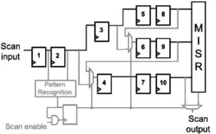
Figure 1. Proposed scan tree architecture Figure 1 describes the proposed architecture. A pattern recognition module and multiplexors are used to pass automatically during the test phase from the ST mode to the SS mode. A MISR is employed to compact the circuit response in ST mode. An output multiplexor allows to choose between the MISR output (ST mode) and the output of scan cell #10 (SS mode).
In ST mode, the test data goes through the scan input and then through scan cells 1, 2, 3-4 (in the same time), 5-6-7 (in the same time) and so on. Thus, in ST mode the scan cells 3 and 4 receive exactly the same test data (and also scan cells 5-6-7 and 8-9-10). In SS mode the test data goes from the scan input to scan cells 1, 2, 3, 5, 8, 6, 9, 4, 7 and finally 10.
A scan tree generation method is required to determine which part of the test sequence must be applied in ST mode and which part in SS mode. The next sub section presents the scan tree generation technique.
2.2 Scan tree generation
The scan tree generation method must find the good balance between the part of the test sequence to apply in ST mode and the other part in SS mode. The scan tree generation technique allows to obtain a solution which requires a minimal test application time.
From a test pattern, we can construct a scan tree architecture using an incompatibility graph and adopt a vertex coloring process for the graph to solve the problem of finding optimal groups of compatible scan cells. In an incompatibility graph for a test pattern, a vertex corresponds to a scan cell, and an edge exists between two vertices if two scan cells corresponding to the vertices are incompatible in the test pattern.
t1: 1 0 0 X X 0 1
2
3 4
5
6 2
3 6 1
5 4
scan input
scan output M
I S R L1=2
Coloring graph Scan tree architecture
1 2 3 4 5 6
t1: 1 0 0 X X 0 1
2
3 4
5
6 2
3 6 1
5 4
scan input
scan output M
I S R L1=2
Coloring graph Scan tree architecture
1
1 22 33 44 55 66
Figure 2. Scan tree generation from a test pattern
M I S R Scan
input
Scan output Pattern
Recognition
Scan enable
1 2
3
5 8
9
10 4
6
7
M I S R Scan
input
Scan output Pattern
Recognition
Scan enable
1 2
3
5 8
9
10 4
6
7
In the example shown in Figure 2, each bit of the test pattern t1 corresponds to a scan cell. The scan tree architecture is generated via a coloring graph from the test pattern t1. Without considering incompatibilities between the bits of t1, the length of the scan tree is equal to 1. In fact, t1 has incompatibilities (1-2 1-3 and 1-6) that are reported on the coloring graph by edges between the node 1 and the nodes 2, 3 and 6. The scan tree length is equal to 2 considering the incompatibilities of t1.
A test pattern selection must be performed to select the test pattern to apply in ST mode. In order to reduce the computation time, the sequence is sorted according to the number of incompatibilities of each test pattern. The test pattern selection corresponds to a Traveling
Salesperson Problem (TSP [22]). The complexity of the problem depends on the number of test patterns and on the scan chain length. A greedy algorithm with a complexity of O(m2) (m being the number of test patterns) is used. The complexity of the coloring process is O(n2) with n being the number of scan cells. Thus, the scan tree generation complexity is O(m2*n2). The selection consists of integrating another test pattern from the initial test pattern (with the less number of incompatibilities). The test pattern which has a lower impact on the scan tree architecture length is chosen. Now, from the solution composed by the two test patterns selected, we try to integrate another one and choose the test pattern with a low impact on the scan tree architecture length. The operation is repeated until all test patterns are integrated in the solution. The last operation consists of identifying the solution which proposes the minimal test application time. More details are given in [19].
This scan tree generation solution requires an important computation time for large circuits. A solution to reduce the computation time consists of using directly the test sequence ordering according to the number of incompatibilities (without greedy algorithm). In this case, the complexity becomes O(m*n2). This solution has great benefit on the computation time according to the complexity. In Section 4, we propose a comparison between the two methods to show the impact of this solution on test application time reduction.
3. Fanout and area optimizations
In this section, we apply different optimizations to decrease scan tree architecture penalties on the performance and DFT area with no modification of the scan tree length. Note that it is also possible to reduce the size of interconnections between scan cell as well as the additional routing which has an impact on the circuit area [21].
3.1 Fanout optimization
The fanout optimization allows to reduce the penalty on circuit performance of the proposed architecture. Indeed, scan cell can drive several scan cells in the scan tree architecture.
The fanout optimization consists of modifying scan cell allocation from a group of scan cells to another group if the scan cell is compatible. Different parameters must be setup: maximal fanout and critical scan cells. Maximal fanout is the maximal number of scan cells that a
scan cell can drive with no modification of the circuit performance. Some scan cells in the design can be considered as critical scan cells if there are included in a critical path. In this case, we can impose a fanout equal to 1 for the critical scan cells.
Figure 3 shows an example of fanout optimization with a maximal fanout parameter equal to 2 and an empty critical scan cell list. In this example, before optimization the fanout of the scan cell 2 is equal to 3. So the optimization consists in finding a scan cell compatible with scan cells 2 or 1 in the group of scan cells composed by the scan cells 3, 4, and 5. The scan cell 5 is compatible with the scan cell 2. Thus, the allocation of the scan cells 5 is changed as shown in Figure 3 (scan tree after fanout optimization). The modification allows to obtain a maximal fanout equal to 2.
3 4 5 2
scan input
scan output M
I S R Scan tree 5
architecture before fanout optimization
Scan tree architecture after fanout optimization
1 3
4 2
scan input
scan output M
I S R 1
5 3
4 5 2
scan input
scan output M
I S R Scan tree 5
architecture before fanout optimization
Scan tree architecture after fanout optimization
1 3
4 2
scan input
scan output M
I S R 1
5
Figure 3. Example of fanout optimization
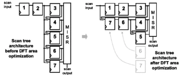
3.2 DFT area optimization
The DFT area optimization consists in minimizing the extra logic required for the proposed architecture (multiplexors used to obtain the dynamic reconfiguration and the MISR). We do not consider the pattern recognition module in this optimization.
The DFT area optimization consists in obtaining scan cell groups of the same size. In this case the size of the MISR and the number of multiplexors are minimal.
3 4 5 1
6 2
scan input
scan output M
I S R
7
3 4 5 1
6 2
scan input
scan output
M I S R
7
7 6
Scan tree architecture before DFT area
optimization architectureScan tree
after DFT area optimization 3
4 5 1
6 2
scan input
scan output M
I S R
7
3 4 5 1
6 2
scan input
scan output
M I S R
7
7 6
3 4 5 1
6 2
scan input
scan output M
I S R
7
3 4 5 1
6 2
scan input
scan output
M I S R
7
7 6
Scan tree architecture before DFT area
optimization architectureScan tree
after DFT area optimization
Figure 4. Example of DFT area optimization In Figure 4, the scan tree architecture before DFT area optimization has a MISR with a size equal to 5, and 4 multiplexors. After the DFT area optimization, the size of the MISR previously equal to 5 is now equal to 3 and the number of multiplexors pass from 4 to 2. The DFT area optimization is possible because scan
Table 1. Experimental results on ISCAS`89 benchmark circuits – Uncompacted test sequence
Previous technique Proposed technique
Benchmark reference
# FFs # test patterns
FC (%)
Test application time reduction (%)
Computation time (sec)
Test application time reduction (%)
Computation time (sec)
s5378 179 166 98.7 72.7% 11 72.2% 1
s9234 211 341 93.2 58.3% 97 57.2% 6
s13207 669 540 98.3 87.8% 548 87.9% 27
s35932 1728 2835 88.6 99.5% 3940 99.1% 481
s38584 1426 1275 95.1 86.9% 14525 86.9% 397
Table 2. Experimental results on ISCAS`89 benchmark circuits – Compacted test sequence
Previous technique Proposed technique Benchmark
reference
# test patterns
FC (%)
Test application time reduction (%)
Test application time reduction (%)
s5378 125 98.7 79.9 80.7
s9234 228 93.2 42.7 46.3
s13207 347 98.3 72.5 71.8
s35932 112 88.6 90.1 95.4
s38584 330 95.1 60 73.3
cells 6 and 7 are compatible with scan cells 2 and 1 respectively. So the allocated group of scan cells 6 and 7 is changed.
We propose two optimizations for our scan tree design with no modification of the test application time. It is possible to improve the scan tree design with a modification of the scan tree length. In the next section, we propose different results concerning the fanout and DFT area optimizations.
4. Experimental results
We have implemented the proposed method and the different optimizations in C language on a Pentium IV 2.8 GHz with 1 GB of memory and have applied it to ISCAS’89 benchmark circuits. The test sets used are provided by Testgen tool [23] from Synopsys.
Table 1 presents the results in term of test application time reduction (corresponding to the number of clock cycles required for the shift operations) and computation time for the proposed scan tree architecture with the two generation techniques. The first columns of the table describe the circuits names, the numbers of scan cells, the lengths of test sequences (without any compaction: uncompacted) and the fault coverage. The following columns present the test application time reduction and the computation time for the previous and new (test sequence ordering only) generation techniques. The test application time reduction allows one to compare the proposed scan tree architecture and the standard scan architecture. The test application time is really similar as one obtained with the previous generation technique. The average
difference concerning the test application time between the two techniques is equal to 4.8%. The computation time with the new generation technique is drastically less important for all circuits. The computation of new generation is up to 36 times less important than the previous technique. So the new generation technique is a good alternative to obtain a solution with a short computation time and a low impact on the test application time.
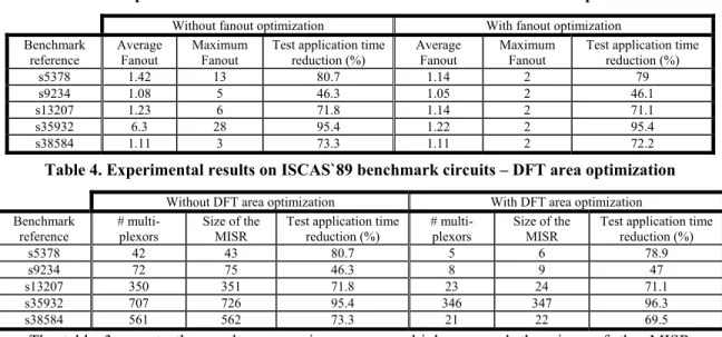
Table 2 presents the results concerning the previous and the new generation techniques in term of test application time reduction with a compacted test sequence. The test application time reduction is a comparison between the compacted test sequence applied in standard scan architecture and a specific compacted test sequence applied in the proposed scan tree architecture. The specific compacted test sequence for the proposed scan tree architecture is obtained from the uncompacted test sequence by a test pattern dropping process. In fact from the uncompacted test sequence, we replace the
“don’t care value” according to the scan tree architecture. After fault simulation, redundant test patterns are removed. The first columns of the Table 2 give the circuit names, the lengths of compacted test sequences and the fault coverage. The two following columns present the test time application reduction for the previous and new generation techniques. The test application time reduction is similar to uncompacted test sequence results. The maximum is 95.4% with the new generation technique. These results confirm the great effectiveness of the proposed architecture to reduce the test timeapplication.
Table 3. Experimental results on ISCAS`89 benchmark circuits – Fanout optimization
Without fanout optimization With fanout optimization Benchmark
reference
Average Fanout
Maximum Fanout
Test application time reduction (%)
Average Fanout
Maximum Fanout
Test application time reduction (%)
s5378 1.42 13 80.7 1.14 2 79
s9234 1.08 5 46.3 1.05 2 46.1
s13207 1.23 6 71.8 1.14 2 71.1
s35932 6.3 28 95.4 1.22 2 95.4
s38584 1.11 3 73.3 1.11 2 72.2
Table 4. Experimental results on ISCAS`89 benchmark circuits – DFT area optimization
The table 3 reports the results concerning the fanout optimization. The scan tree architecture is generated with the new generation technique. The first column gives the circuits names. The three following columns give the details concerning the proposed architecture without fanout optimization in terms of average fanout, maximum fanout and test application time reduction (compacted test sequence). The three last columns report the same details concerning the proposed architecture with fanout optimization. We use a maximum fanout parameter equal to 2 and with no critical scan cell as parameters. The average fanout corresponds to the average number of scan cells that a scan cell drives in the design. The result shows a reduction of the average fanout equal in standard to 22.1%. The maximum fanout, which is the maximum number of scan cells that a scan cell drives in the design with no modification of the circuit performance, is reduced in standard of 60.9%. So the maximum fanout parameter is respected. Moreover, the fanout optimization requires change the scan cell group assignation in the design. This modification has no effect on the scan tree length. However, there is a modification of the test application time reduction for compacted test sequence due to the change of scan cells assignment. In maximum, the test application time reduction decrease less than 2%. All these results confirm the effectiveness of the fanout optimization solution. The table 4 gives the results concerning the DFT area optimization. The scan tree architecture is generated with the new generation technique. The table 4 has the same organization of the table 3. Instead of the average fanout and the maximum fanout, the numbers of
multiplexors and the sizes of the MISR are reported. DFT area optimization allows one to reduce the number of multiplexors of 83.6% in standard. Concerning the size of MISR, the reduction is in standard equal to 83.1%. There is also a modification of the test application time reduction due to the scan cell assignment modification. The test application time reduction decreases less than 3%.
Without DFT area optimization With DFT area optimization Benchmark
reference
# multi- plexors
Size of the MISR
Test application time reduction (%)
# multi- plexors
Size of the MISR
Test application time reduction (%)
s5378 42 43 80.7 5 6 78.9
s9234 72 75 46.3 8 9 47
s13207 350 351 71.8 23 24 71.1
s35932 707 726 95.4 346 347 96.3
s38584 561 562 73.3 21 22 69.5
All these results show that the proposed scan tree architecture is a possible alternative to multiple scan based architecture. Moreover, different optimizations can be performed successfully. These optimizations can be applied separately or concurrently to improve the proposed scan tree design.
5. Extension: Test power reduction
Scan based architecture can lead an excessive test power consumption. This elevated test power may be responsible for several kinds of problems as instant circuit damage and decrease of overall yield. A survey of these problems is given in [2].
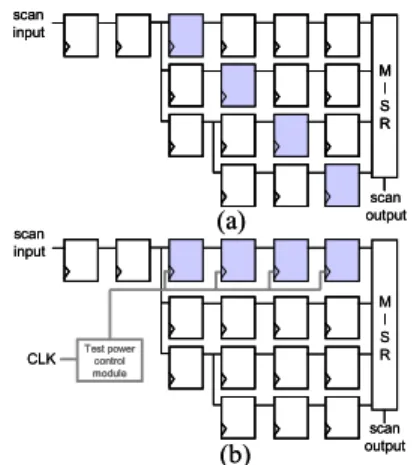
We propose an extension to the proposed scan tree architecture to reduce test power. During the test phase, the full observability and full controllability is not required all the time. Some scan cells are not used during part of the test phase. We propose a solution to disable these scan cells based on branch disable technique. The figure 5 shows an example. The scan cells in grey are in used during all the test phase (figure 5.a). The figure 5.b describes the scan cell position modification process. The modification process consists of grouping all the scan cells in grey in the same branch. In this case with a test power control module, it is possible to
disable this branch during a part of the test phase. The disable solution is based on a gated clock technique which has the advantage to reduce the clock power.
Figure 5. Example of test power insertion Moreover the scan cell modification process can change the position of a scan cell in the group or change the scan cell group assignment. In future work, we will propose the complete solution to consider the test power reduction.
6. Conclusion
In this paper, we propose different improvements of our scan tree architecture in term of generation process to reduce the computation time, the fanout and the extra DFT area. Experimental results show the great benefit of all these improvements. In future work, we shall provide the complete solution to reduce the test power and consider design constraints.
Acknowledgments
This work was supported in part by 21st Century COE (Center of Excellence) Program
"Ubiquitous Networked Media Computing" and in part by JSPS (Japan Society for the Promotion of Science) under Grants-in-Aid for Scientific Research B(2) (No. 15300018).
References
[1] M.L. Bushnell and V.D. Agrawal, “Essentials of Electronic Testing ”, Kluwer Academic Publishers, ISNB 0- 7923-7991-8, 2000.
[2] P. Girard, “Survey of Low-Power Testing of VLSI Circuits”, IEEE Design & Test of Computers, Vol. 19, N° 3, pp. 82-92, May-June 2002.
[3] P.P. Fasang, J. P. Shen, M. A. Schuette and W. A. Gwaltney, “Automated Design for Testability of Semicustom Integrated Circuits”, IEEE Int. Test conf. pp. 558-564, November 1985.
[4] S. Kobayashi, M. Edahiro and M. Kubo, “Scan-Chain Optimization Algorithms for Multiple Scan-Paths”, IEEE Asia and South Pacific Design Automation Conf., pp. 301- 306, February 1998.
[5] S. Narayanan, R. Gupta and M. A. Breuer, “Optimal Configuration of Multiple Scan Chains”, IEEE Trans. On Computers, Vol. 42, N° 9, pp. 1121-1131, September 1993. [6] S. Bhawmik and P. Palchaudhuri, “DFT Expert: Designing testable VLSI Circuits”, IEEE Design Test, pp. 8- 19, October 1989.
M I S R
M I S Test po R
Test powerwer control control module module scan input
scan output scan
input
CLK
scan output
(a)
(b)
M I S R M I S R
M I S Test po R
Test powerwer control control module module scan input
scan output scan
input
CLK
scan output
(a)
(b)
[7] J. Rajski, J. Tyszer, M. Kassab, N. Mukherjee, R. Thompsom, K. H. Tsai, A. Hertwig, N. Tamarapalli, G. Mrugalski, G. Eide and J. Qian, “Embedded Deterministic Test For Low Cost Manufacturing Test”, IEEE Int. Test Conf., pp. 301-310, October 2002.
[8] A. Chandra and K. Chakrabarty, “Frequency-Directed Run-Length (FDR) Codes with Application to System-on-a- chip Test Data Compression”, IEEE VLSI Test Symp., pp. 42-47, April 2001.
[9] A. Jas, J.G. Dastidar and N.A. Touba, “Scan Vector Compression /Decompression Using Statiscal Coding”, IEEE VLSI Test Symp., pp. 114-120, April 2000.
[10] A. Jas, B. Pouya and N.A. Touba, “Virtual Scan Chains’ A Means for Reducing Scan Length in Cores”, IEEE VLSI Test Symp., pp. 73-78, April 2000.
[11] S. Sybille, H.G. Liang and H.J. Wunderlich, “A mixed Mode BIST Scheme Based on Reseeding of Folding Counters”, IEEE Int. Test Conf., pp. 778-784, October 2000. [12] W.B. Jone, J.C. Rau, S.C. Chang and Y.L. Wu, “A Tree- Structured LFSR Synthesis Scheme for Pseudo-Exhaustive Testing of VLSI Circuits”, IEEE Int. Test Conf., pp. 322-330, October 1998.
[13] I. Bayraktaroglu and A. Orailoglu, “Test Volume and Application Time Reduction through Scan Chain concealment”, Design Automation Conference, pp. 151-155, June 2001.
[14] I. Hamzaoglu and J. H. Patel, “Reducing Test Application Time for Full Scan Embedded Cores”, Int. Symp. on Fault Tolerance Computing, pp. 260-267, July 1999.
[15] A.R. Pandey and J. H. Patel, “Reconfiguration Technique for Reducing Test Time and Test Data Volume in Illinois Scan Architecture Based Designs”, IEEE VLSI Test Symp., pp. 9-15, April 2002.
[16] K.L. Lee, J.J. Chen and C.H. Huang, “Using a Single Input to Support Multiple Scan Chains”, ICCAD, pp. 74-78, November 1998.
[17] K. Miyase and S. Kajihara, “Optimal Scan Tree Construction with Test Vector Modification for Test Compression”, IEEE Asian Test Symp., pp. 136-141, November 2003.
[18] H. Yotsuyanagi, T. Kuchii, S. Nishikawa, M. Hashizume and K. Kinoshita, “Reducing Scan Shifts using Folding Scan Trees”, IEEE Asian Test Symp., pp. 6-11, November 2003. [19] Y. Bonhomme, T. Yoneda, H. Fujiwara and P. Girard,
"An Efficient Scan Tree Design for Test Time Reduction," Proc. 9th IEEE European Test Symposium (ETS'04), pp. 321-326, May 2004
[20] D. Xiang , S. Gu, J. G. Sun and Y. Wu, “A Cost- Effective Scan Architecture for Scan Testing with Non-Scan Test Power and Test Application Cost”, Design Automation Conf., pp. 744-747, June 2003.
[21] Y. Bonhomme, P. Girard, L. Guiller, C. Landrault and S. Pravossoudovitch, “An Efficient Scan Chain Design for Power Minimization During Scan Testing Under Routing Constraint”, IEEE Int. Test Conf., pp. 488-493, October 2003.
[22] D.S. Johnson and L.A. McGeoch, “The Traveling Salesman Problem : A Case Study in Local Optimization”, in Local Search algorithms in Combinatorial Optimization, E.H.L. Aarts and J.K. Lenstra, eds. John Wiley and Sons, 1996.
[23] TestGen, Version 5.3, Synopsys Inc., 1999.