Power-Conscious Multi-Frequency Modular Testing of SoCs with Dynamic
Reconfiguration of Multi-Port ATE
∗Dan Zhao and Ronghua Huang Center for Advanced Computer Studies
University at Louisiana at Lafayette {dzhao,rxh2888}@cacs.louisiana.edu
Tel: 337-4826875, Fax: 337-4825791
Hideo Fujiwara
Graduate School of Information Science Nara Institute of Science and Technology
Tel: +81-743-725220, Fax: +81-743-725229
Abstract— With the debut of a new class of multi-port ATE (e.g., Agilent 93000 series), there is a pressing need for test plan- ning methods to fully adapting SoC test framework design to the new concurrent test capabilities and fulfil emerging demands of high-speed testing. In this paper, we propose a new test planning strategy that addresses multi-frequency SoC testing by dynam- ically reconfiguring ATE ports. The system integrators on-the- fly group pins into virtual ports while ATE ports simultaneously drive the testing of a set of cores at multiple independent clock do- mains. An effective and efficient system optimization technique is developed to manage test resources and improve test efficiency for modern complex SoC designs.
keywords: Concurrent Test, Multi-Frequency SoC Test, Test Resource Partitioning, ATE Port Reconfiguration, Constrained Scheduling
I. INTRODUCTION
State-of-the-art Systems-on-Chip (SoCs) embed pre- designed and pre-verified functional modules from various intellectual-property (IP) providers, and integrate them within a single silicon system to provide complex functionality, high performance, low power and small form factor. As the complexity, heterogeneity and speed of SoCs continue to rise rapidly, the test cost-per-transistor, unlike manufacturing cost-per-transistor, has not tracked Moore’s Law. The SoC trends that increase test cost are: (1) the number of cores and their terminals are increasing much faster than the chip pins that limits ATE access to the IP cores; (2) An increase in speed-related defects acquires at-speed fault detection; (3) the increasing heterogeneous and hierarchical integration pushes the need for different test speeds to address multi-clock domain issues among different cores; (4) different core re- quires different test method and test application time, and thus requires tremendous flexibility in test architecture; (5) longer testing time accounts for increasing complex SoC designs.
To ensure that test cost scales with Moore’s Law, it calls for a new design-for-concurrent-test strategy where an SoC is viewed as a collection of embedded heterogeneous cores with different testing requirements, tested concurrently. The
∗This research is supported in part by LA BORSF Research Competitive Subprogram.
move from traditional shared-resource ATE architecture to new multi-port ATE architecture (such as Agilent 93000 series [1]) allows that multiple pins are grouped into virtual ports to test individual cores in parallel. The ports will be immediately re- configured upon completion of one concurrent test session and initiate the next set of concurrent core testing until the SoC is completely tested. Moreover, multiple ports can indepen- dently operate multiple tests at different test speeds. Such a flexible per-port architecture allows different test pins to op- erate in different modes to fulfil comprehensive SoC test re- quirements thus improving test efficiency. To adapt an SoC design to ATE concurrent test capabilities, the system integra- tor needs to design appropriate test access architecture (TAM) to transport test data to the embedded core-under-test (CUT). The CUT needs to be completely isolated (from the rest of the chip) and independently accessed via core test wrapper (e.g. IEEE std. 1500 wrapper).
A significant amount of research has been conducted [2, 3, 4, 5, 6, 7] as shown in the literature to design and optimize core test wrappers and/or TAMs. Consequently, constraint-driven test scheduling problems have been studied to minimize SoC test cost in terms of test application time. Such optimization problems have been proven N P -hard by reducing into any in- stance of Bin Design and Multi-Processor Scheduling prob- lems and thus fast heuristics have been developed to solve it. However, all these approaches are only applicable to single frequency modular SoC testing where all cores are tested at a single low ATE clock. Modern SoCs are typically embedded with modular IP cores operated in multiple clock domains and moreover, multiple internally generated clocks. To improve test efficiency, using multiple frequencies is a benefit over sin- gle frequency testing due to the ability to offer comprehensive fault detection.
Recently, a few initial attempts [8, 9, 10, 11] have been made to address multi-frequency wrapper/TAM design and op- timization for multi-clock domain SoC testing. However, these approaches assume that the ATE delivers test data at a sin- gle data rate. With the debut of a new class of multi-port ATE, there is a pressing need for test planning methods to fully exploit the new concurrent test capabilities of these ATEs and fulfil emerging demands of high-speed testing. A recent work [12] on TAM optimization has introduced the use of dual- IEEE 16th Asian Test Symposium (ATS'07), pp.107-110, October, 2007.
speed ATEs that drives the channels at two different speed. The test scheduling is performed by packing rectangle tests into pre-partitioned high-speed and low-speed bins. Although this approach doesn’t fully utilize the flexible per-pin architecture that supports tremendous capability to dynamically reconfig- ure ports, this work is a promising first step in this direction.
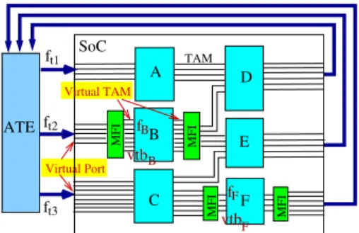
We propose a new test planning strategy that addresses multi-frequency SoC testing by fully exploiting multi-port ATE concurrent test capabilities. As the per-pin architecture provides the flexibility to dynamically match ATE ports to SoC’s pin-out, the system integrator can on-the-fly group pins into virtual ports to test individual cores that have various test- ing requirements as illustrated in Figure 1. These virtual ports simultaneously drive the testing of a set of cores at multiple in- dependent clock domains. Upon completion of any test appli- cation, the freed-up pins are dynamically reconfigured to ini- tiate other tests immediately. Multi-frequency interface (MFI) is properly designed and inserted when there is a mismatch between the ATE port capability and core test data rate. Vir- tual test buses are connected to the core terminals via MFI. The bandwidth matches at both sides of MFI. An efficient test resource management technique should be developed, that in- volves various aspects, such as dynamic ATE port reconfig- uration, the routing of TAMs, the design of multi-frequency test interface, the configuration of core wrapper scan architec- ture, and the distribution of bandwidth and power budget. In this paper, we propose a system level optimization technique to ease test integration, to facilitate concurrent test to the max- imum extent, and to efficiently partition test resources to fulfil demanding performance and cost challenges.
SoC
ATE
MFI
MFI
MFI
MFI
F E D
C B
A TAM
vtbF Virtual TAM
Virtual Port
ft1
ft2
ft3
fB
fF vtbB
Fig. 1.Hypothetical illustration of concurrent test planning with multi-port ATE.
The rest of the paper is organized as follows. In Sec. IIA, we design a multi-frequency interface for virtual port configu- ration and virtual TAM assignment. The core wrapper config- uration is studied in Sec. IIB. Then we formulate the system optimization problem into 3-D bin packing in Sec. IIC and pro- pose an efficient heuristic algorithm to design and optimize the test framework with resource partitioning and test scheduling to minimize test cost in Sec. IID. The promising of the pro- posed optimization technique is confirmed in Sec. IIE where we run extensive simulation and comparison. Finally we con- clude the paper in Sec. III.
II. MULTI-SPEEDTAM DESIGNWITHPORT
RECONFIGURATION
A. Design of Multi-frequency Interface
The multi-frequency interface design problem is basically to determine virtual port configuration on one hand and core wrapper configuration on the other hand.
Due to the heterogeneity of SoC integration, different cores may have different test requirement, and thus be tested at dif- ferent clock rate. Some cores require specific test data rate and are driven by certain ATE ports. While the others do not set re- striction on scan speed thus have the flexibility to operate under various clock domains and can be assigned to any port. A set of distinct frequencies derived from ATE clocks (using hardware division logic) forms the candidate frequency set for the cores. To provide a wide range of frequency selection improves test efficiency from two aspects. On one hand, it can save power dissipation when setting core test data rate lower than the ATE port. On the other hand, it can reduce the test time by running at higher clock rate. However, multi-frequency testing results in a frequency gap at the core interface between core wrap- per scan architecture and core-external test access mechanism (TAM), and accordingly low utilization of bandwidth (defined as the product of data frequency and data transportation width). In order to resolve the mismatch between ATE capability and core test speed, a multi-frequency test interface (M F I) is de- signed that synchronizes input/output data and transfers test patterns/responses into/out of the corresponding scan-enabled core.
Assume the ATE supports Npt ports at various clock do- mains fti, i∈ Npt. Using port ptias an example that consists of a set of ATE channels at clock domain fti. The test data is transported from/to certain ATE channels along parallel TAMs with width of Wtami and frequency of fti (where Wtami is the width of port pti). The bandwidth Wtami × fti is dis- tributed to one or multiple cores at distinct frequency via pairs of multi-frequency interface where it is necessary. A ATE port is thus divided into several virtual ports, each connecting to a core. Virtual TAMs connect core (say B) terminals to M F I at chosen width and core test frequency of wvtbB and fBre- spectively. The dedicated TAM width for a core (or the virtual port width) is determined by wvpB = wvtbBf ×fB
ti . As multiple cores can be assigned to the same ATE port and tested concur- rently, it should satisfy that Σmj=1wvpj ≤ Wtami. Note that, as the chip level TAM width Wextis constrained by the SoC pin count, ΣNi=1ptWtami≤ Wext.
The bandwidth matching is performed in consequence via multi-frequency interface (e.g. MUX-DeMUX). If test data rate fBfor core B is higher than fti, we insert a MUX before core input terminals, and multiplex⌈ffB
ti⌉ × wvtbB bits test data at fti into wvtbB bits test data at fB. On the other hand, if fB
for core B is lower than fti, we insert a DeMUX instead, and de-multiplex wtamB bits test data at fti into wtamB × ⌊fftiB⌋ bits test data at fB. To observe test responses, we insert De- MUX/MUX accordingly after core output terminals. Multi- frequency interface design facilitates SoC test cost reduction in
a way that co-optimizes both core wrapper configuration, core test frequency selection and virtual port partitioning to achieve the best tradeoff among them.
B. Core Wrapper Confi guration
Core wrapper architecture is configured to minimize the test time by constructing wrapper scan chains in a way that their length are well balanced as the longest wrapper scan chain dominates the test time. The wrapper scan width of a scan- testable core is adapted to the core-external TAM width (i.e. wvtb) by serially connecting core inputs/output terminals to the internal scan chains. In order to balance the wrapper scan chain lengths so as to minimize the maximum wrapper scan chain length (Lmax), bin design based fast heuristics such as FFD and BFD [2, 6] are proposed to solve it. Thus we obtain a finite set of wrapper configuration candidate set for each core with decreasing Lmax at increasing wvtb, i.e. Ri(wvtbi, Lmaxi) (where Ri denotes a distinct wrapper configuration). As the test time for a core given test pattern is a function of the longest wrapper scan chain length and the scan frequency, the increase of wrapper scan chain width itself decreases the test time, while the test time reduces with the increase of frequency. With the flexibility to choose from a candidate set, it facilitates efficient test scheduling where the most suitable wrapper con- figuration will be selected for a core to fit into the available idle space.
An important observation is made from the wrapper candi- date set of a core. That is doubling the width of a core, the rect- angle area obtained by multiplying Lmaxand wvtbincreases or remains the same. This observation has been confirmed with all scan-testable cores in ITC SoC benchmarks [13]. No doubt, a fact arises that by halving the shift frequency the shift time may increase or remain the same when matching the band- width. With this feature, more flexible scheduling may be achieved by relieving tight power budget without increasing the test time as explained next in the optimization approach.
C. Problem Formulation
In this section, we define the power-conscious multi-speed TAM design (P M F T ) problem and formulate it into 3-D bin packing.
Without loss of generality, we assume an SoC model S em- bedded with NcIP cores C = {ci|i = 1...Nc}. Each core is given a set of test parameters including the number of core input/output/bidirectional terminals, the number of test pat- terns, the number of internal scan chains and their lengths, the test power obtained at maximum allowable frequency, and the functional frequency. The cores are given a set of test fre- quency candidates derived from the ATE clocks. Each core can select a proper wrapper design at certain test data rate, thus a core ciis expressed as a three-tuple ci= {ti, pi, wvpi}, where tiis the test time obtained at width of wvtbiand test fre- quency fci, piis the test power of cidissipated at frequency fci, wvpiis the virtual port width assigned to core ci. In addi- tion, the SoC is given a chip level TAM width of Wextand a
power budget of Pave. Assume a multi-port ATE supports up to Nptports, each corresponding to a independent clock do- main fti, i ∈ Npt. The port width is dynamically assigned during scheduling. But the total port width should not exceed Wext. The optimization problem is stated as follows:
P M F T Problem: Given an SoC model S with NcIP cores, a chip level TAM width Wext, and the maximum average power allowance Pave, and given a multi-port ATE with up to Npt distinct clock domains, determine (1) dynamic group- ing of ATE channels into several ports to deliver test data at different test speed, (2) the multi-frequency interface, test data rate and wrapper configuration of each core, and (3) a con- strained test scheduling that parallel routes multiple cores on TAMs such that the overall SoC test time is minimized while satisfying power and chip level TAM constraints at any time.
We define a 3-D bin with the height of the overall SoC test time, and its length and width bounded by the power Paveand TAM width Wextconstraints respectively. The cubes of cores may overlap in time dimension for concurrent testing but not the power and TAM width dimensions. The P M F T problem is thus reduced into 3-D bin packing: Given a set of core tests represented in cubes, find a way to packing the cubes into a 3- D bin bounded by the bottom, so as to minimize the height to which the cubes fill the bin. It is easy to reduce such bin pack- ing problem into any instance of the partitioning problem [14], thus is N P -hard. An effective and efficient heuristic algorithm is developed thereafter.
D. Advanced Shelf Packing Based Optimization Algorithm The proposed algorithm has four major steps, namely, initial packing in shelf S1, ceiling packing in idle bins, floor packing in shelf S2, and halved floor packing. In this section, we give an intuitive description of the steps and illustrate the approach with a hypothetical example.
A pre-processing step is performed first to obtain the can- didate wrapper set for each core Rki = {wkvtbi, Lkmaxi} by running best-fit decreasing heuristic. Different combinations of wvtbk i and Lkmaxiprovides the flexibility to make the trade- off between several interdependent design items, such as test power, test time and core-external TAM width, thus results in the best selection possible in terms of the configuration of the three dimension of a cube.
Step 1: Initial Packing in Shelf S1
We first obtain an ordered cube list to initiate packing. We try to find the maximum possible test data rate fcimax for core ci from a range of frequency selection at which test- ing is performed without exceeding the power constraint, i.e., pi(fcimax) = fci maxF ×P owi
max ≤ Pave. Then we find a proper wrapper design via bandwidth matching, i.e., wvtbi ≤
max{ftj}×Wext
Npt×fci max , which results in the initial test time ti iniand virtual port width wvpi for ci, respectively. After we obtain the initial setting of a cube, an additional checking process is applied. We reduce the width of those cubes whose initial width exceeds βWext (where0.5 < β < 1) such that their
newly selected widths mostly close to βWextwithout exceed- ing it. Their initial test times are updated accordingly. We may further reduce the test power for a core without affecting its initial test time by employing the observation as discussed in Sec. IIB. If the initial test time remains the same each time when halving the frequency, the test power and virtual port width will be updated as well. Note that, the new width should not exceed βWext. By freeing up more idle power, we may accommodate more cubes at one time without exceeding tight power budget. Two ordered lists are obtained, one is in the de- scending order of ti ini, i.e. Lt= {ti ini} and the other in the descending order of wvpi, i.e. Lw = {wvpi}.
We start packing in a way that picks the cubes one by one from Lw whose width falls within the range of 0.5Wext to βWext and stack at the bottom of the bin one on top of the other in time dimension. A hypothetical example in Figure 2 illustrate the schedule after the first step.
ext floor
ceiling
S1
IB IB2
IB1
3
IB2+ IB1
1/2 Wext W
A B C
Fig. 2.Hypothetical illustration of initial packing.
Step 2: Ceiling Packing in Idle Bins
After the first step, we say the allocated cubes are in the first shelf of the bin and we name the bottom edge, the shelf floor and the top edge, the shelf ceiling. In order to efficiently uti- lize the idle space left in this shelf, we divide the idle space into several idle bins IB[1..Nib] from right to left as shown in Figure 2. The height, length and width of each idle bin is determined by the size of the associated cubes. For instance, cores A, B and C are packed into the shelf from floor to ceil- ing, where tB > tA > tC, wtpA > wtpB > wtpC and pB > pC> pA. The height of IB1is the height of the shelf, i.e. the sum of the test time of these cores H(IB1) = tA+ tB+ tC. Its width is determined by the longest cube width W(IB1) = Wext− wvpA, and its length is determined by the most power- consuming core L(IB1) = Pave − pB. Similarly, we can calculate the size of other idle bins. In order to best-fit un- scheduled cubes into these idle bins, we consider a total of Nib
combinations of idle bins in the order of{IB1}, {IB2+IB1}, {IB3+ IB2+ IB1}, ..., {IBNib+ IBNib−1+ ... + IB1}. The size of each combination of the idle bins is computed accord- ingly. For a particular combination, its height and length are determined by the smallest height idle bin in the group and its width is the sum of the width of these idle bins as shown in Figure 2.
We start allocating unscheduled cubes in the order of Ltand try to fit one at a time in the sequence of all combinations of idle bins. The idea is that we pick the first available combina- tion of idle bins, CIBjj ∈ Nib, and search through the core
list to find the best-fit cube that can utilize the idle bin to the maximum extent. If no cube fits, we try the next combination, so on and so forth.
More specifically, for a certain combination of idle bins, say CIBj, we pick the first unscheduled core in Ltwhose height fits CIBj. Its width will be checked next. If the initial cube width exceeds the width of CIBj, we try to reduce the wrapper scan chain width of the core in a way that the induced increase in test time won’t lead to an excess of the height of CIBj. If no suitable width can be found when we search through the candidate wrapper configuration list, we move on to the next unscheduled core in Lt, otherwise, we further check the power consumption. If the initial test power exceeds the length of CIBj, we try to reduce the power by reducing its frequency following the frequency list. Again, the induced increase in test time should meet the height limit of CIBj. If no proper frequency is found, we move on to the next core. Otherwise, the cube will be allocated in CIBj justified from right to left with its top edge below the shelf ceiling as shown in Figure 3. If no suitable cube can be allocated in CIBjafter we search through list Lt, a new search of cube will be initiated to fit in the next combination of idle bins, CIBj+1. After a cube is al- located, some idle bins may be eliminated while the remaining are updated with their length and width shortened. For exam- ple as shown in Figure 3, the previous IB1is eliminated while IB2and IB3are updated by shortening its length and width. All available combinations of idle bins are updated by exclud- ing IB1and updating IB2and IB3as well.
We will repeat the above process until no unscheduled cores can be fit into the remaining idle space and we will move on to the third step.
S1
ceiling
floor
IB3 IB2
Wext
Wext
1/2
Fig. 3.Hypothetical illustration of ceiling packing.
Step 3: Floor Packing in Shelf S2
In this step, we pack the unscheduled cubes on top of the first shelf using a floor-packing approach. The basic idea is that a picked cube is packed left on floor justified on the second shelf S2where it fits, and each subsequent ones adjacent to the one just packed as illustrated in Figure 4. More importantly, we need to find a way to pack into S2as many cubes as possible while satisfying tight power and TAM width constraints.
Following the order in Lt, we start allocating unscheduled cubes in shelf S2from the highest cube. The height of S2, H(S2), is determined by the test time of the first allocated cube. Then we try to pack the next highest possible unsched- uled cubes to use up the remaining idle TAM width and power. A fast process to check if a cube can be contained in the shelf
is developed. For an incoming cube, we first check if it satis- fies the power constraint at the minimum available frequency, min{fi}. If it satisfies power limit, we further check if it can meet the height allowance at the initial frequency, fci max.
If it satisfies again, we will pick the best frequency within the range of (min{fi}, fci max) such that its test time at certain wrapper configuration is closest to H(SN) but not exceeding it. The reason is simply to free up more TAM width and power so as to contain more cores. The above process continues until there is no more idle space available or there are no cores left for packing.
S2S1
ceiling
floor
Wext
Wext
1/2 Fig. 4.Hypothetical illustration of floor packing.
Step 4: Halved Floor Packing
After we finish scheduling in shelf S2, we partition the 3- D bin into two halves. Let S2Ldenote the left half shelf with height of H(S2). Let S2R denote the right half, and its height is determined by the highest cube in the right half (or partially in the right half) as shown in Figure 5. All subsequent pack- ing in the left and right halves will occur above the ceiling of these half shelves. Each time we choose the half whose ceiling is lower and create a new half shelf on top of it. We pack the cubes horizontally from left to right into this half bin by ap- plying the floor packing approach as described in Step 3. If no cubes can be fit into this half shelf, we create a new half shelf on top of the half bin whose ceiling is lower. We repeat these process until there are no more cubes.
The overall SoC test time is determined by the higher half bin. For example in Figure 5, the SoC test time is determined by the height of left half bin, i.e., TSoC= H(S1) + H(S2L) + H(S4).
floor ceiling
S1 S3S4 S2R
1/2 Wext Wext S2L
Fig. 5.Hypothetical illustration of halved floor packing.
E. Simulation Study
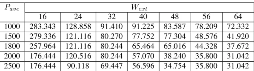
We evaluate the proposed algorithm by running simulations on ITC’02 SoC test benchmarks d281 and d695 where the test power parameters are provided [13]. Each SoC model is em- bedded with a set of IP cores. Each core is provided a set of test parameters, including the number of inputs, outputs and bidirectional terminals, the number of test patterns, the num- ber of scan chains and their length, the test power and the associated test frequency. Some cores have a particular re- quirement on test data rate while the others set no restriction thus can perform testing at various clock domains. A range of candidate frequencies are provides for selection. The example ATE drives test data at three distinct clock domains, 50MHz, 120MHz and 250MHz. We run experiments with chip level TAM width Wextchanging from 16 to 64 (pin count from 32 to 128) while average power budget at 1500, 1800, 2000 and 2500 respectively. The simulation results are listed in Tables I, II.
From the simulation results, we can see that overall SoC testing time reduces when relaxing the power budget or SoC pin-count constraint. When comparing the test time of our ap- proach to the one reported in [10], our approach outperforms this best-fit decreasing based heuristic, that could be reduced to an instance of 3-D bin packing problem. The improvement can reach as high as 44.15%. The reason is simply because we fully utilize the new concurrent test capabilities of multi-port ATE where multiple ports may deliver test data at distinct clock domains. While the approach in [10] assumes that the ATE de- livers test data at a single data rate. Our proposed algorithm requires a negligible amount of computation time (in ms) and therefore is suitable for more complex SoC designs. This is especially an improvement over the CPU-intensive ILP-based method [12].
III. CONCLUSION
We have presented in this paper a novel power-aware multi- speed TAM design by dynamically reconfiguring ATE ports. We have formulated the power-constrained multi-frequency TAM optimization problem into a 3-D bin packing problem. We have further proposed an efficient advanced shelf-packing based heuristic algorithm to manage the test resource partition- ing from various aspects, such as dynamic ATE port reconfig- uration, the routing of TAMs, the design of multi-frequency interface, the configuration of core wrapper scan architecture, and distribution of bandwidth and power budget. By fully ex- ploiting multi-port ATE concurrent test capabilities, SoC test efficiency is significantly improved and test cost is minimized.
REFERENCES
[1] “Agilent debuts multi-clock domain test capabilities for 93000 soc.” www.agilent.com/see/semitestnews.
[2] E. J. Marinissen, S. K. Goel, and M. Lousberg, “Wrapper design for embedded core test,” in Proc. of ITC, pp. 911–920, october 2000.
TABLE I
OVERALL TES T TI M E F ORSOC d281
Pave Wext
16 24 32 40 48 56 64
1000 283.343 128.858 91.410 91.225 83.587 78.209 72.332 1500 279.336 121.116 80.270 77.752 77.304 48.576 41.920 1800 257.964 121.116 80.244 65.464 65.016 44.328 37.672 2000 176.444 120.516 80.244 57.070 38.240 35.800 31.042 2500 176.444 90.118 69.447 56.596 34.754 35.800 31.042
TABLE II
OVERALL TES T TI M E F ORSOC d695
Pave Wext
16 24 32 40 48 56 64
1000 tM P F T 498.364 314.060 270.768 266.232 174.868 152.164 151.36
t[10] 440.00 356.80 273.67 - 264.96 - 247.07
δT (%) -13.26 11.98 1.06 - 34.00 - 38.41
1500 tM P F T 402.700 263.520 222.137 218.921 131.824 123.432 104.304
t[10] 436.05 300.01 222.79 - 180.28 - 162.39
δT (%) 7.65 12.16 0.29 - 26.88 - 35.77
1800 tM P F T 398.788 253.472 190.240 141.104 120.260 116.052 77.724 2000 tM P F T 364.254 214.504 167.330 101.672 86.288 81.672 75.207
t[10] 433.87 304.90 217.31 - 151.37 - 123.76
δT (%) 16.05 29.65 22.30 - 42.99 - 39.23
2500 tM P F T 363.588 214.504 154.488 91.056 84.540 81.672 63.352
t[10] 433.87 299.18 216.77 - 151.37 - 112.93
δT (%) 16.20 28.30 28.73 - 44.15 - 43.90
[3] K. Chakrabarty, “Optimal test access architectures for system- on-a-chip,” ACM Trans. on Design Automation of Electronic Systems, vol. 6, pp. 26–49, January 2001.
[4] Y. Huang, S. Reddy, W. Cheng, P. Reuter, N. Mukherjee, C.-C. Tsai, O. Samman, and Y. Zaidan, “Optimal core wrapper width selection and SOC test scheduling based on 3-D bin packing al- gorithm,” in Proc. International Test Conf., pp. 74–81, October 2002.
[5] E. Larsson and Z. Peng, “Test scheduling and scan-chain di- vision under power constraint,” in Proc. Asian Test Symp., pp. 259–264, november 2001.
[6] V. Iyengar, K. Chakrabarty, and E. J. Marinissen, “Co- optimization of test wrapper and test access architecture for em- bedded cores,” Journal of Electronic Testing: Theory and Appli- cations, vol. 18, pp. 213–230, April 2002.
[7] D. Zhao and S. Upadhyaya, “Power constrained test scheduling with dynamically varied TAM,” in Proc. of VTS, pp. 273–278, April 2003.
[8] Q. Xu and N. Nicolici, “Wrapper design for testing IP cores with multiple clock domains,” in Proc. Design, Automation and Test in Europe Conf., pp. 416–421, February 2004.
[9] A. Sehgal, V. Iyengar, M. D. Krasniewski, and K. Chakrabarty,
“Test cost reduction for SOCs using virtual TAMs and lagrange multipliers,” in Proc. IEEE/ACM Design Automation Conf., pp. 738–743, June 2003.
[10] T. Yoneda, K. Masuda, and H. Fujiwara, “Power-constrained test scheduling for multi-clock domain SoCs,” in Proc. Design, Automation and Test in Europe Conf., pp. 297–302, March 2006. [11] D. Zhao, U. Chandran, and H. Fujiwara, “Design and optimiza- tion of a power-aware multi-frequency wrapper architecture for modular IP cores,” in IEEE Asia and South Pacific Design Au- tomation Conference, pp. 714–719, January 2007.
[12] A. Sehgal and K. Chakrabarty, “Effi cient modular testing of socs using dual-speed tam architectures,” in Proc. IEEE/ACM De- sign, Automation and Test in Europe Conf., pp. 422–427, Febru- ary 2004.
[13] E. J. Marinissen, V. Iyengar, and K. Chakrabarty,
“ITC’02 SOC test benchmarks.” http://www.hitech- projects.com/itc02socbenchm/.
[14] M. Garey and D. Johnsonn, A Guide to the Theory of NP- Completeness. Freeman, San Fransisco, CA.