An Approach to RTL-GL Path Mapping Based on Functional Equivalence
Hiroshi Iwata , Satoshi Ohtake and Hideo Fujiwara
Graduate School of Information Science ,Nara Institute of Science and Technology
8916-5 Takayama, Ikoma, Nara 630-0192 ,Japan
{ hiroshi-i, ohtake, fujiwara }@is.naist.jp
Abstract
Information on false paths in a circuit is useful for de- sign and test. The use of this information may contribute not only in reducing the time required for logic synthesis, circuit area, test generation time and test application time of the circuit, but also in alleviating over-testing. Since identifica- tion of false paths at gate level (GL) is hard for large circuits with a tremendous number of paths, several methods using high-level design information have been proposed. These methods are effective only if the correspondence between paths at register transfer level (RTL) and paths at gate level can be established. Until now, the correspondence has been established only by some restricted logic synthesis. In this paper, we propose a method of mapping an RTL path to its corresponding gate level paths without any specific logic synthesis. The method first maps each bit-sliced RTL signal line of an RTL path to a gate level net by considering the functional equivalence of those signal lines. The RTL path is then mapped to gate level paths using these correspon- dences.
Key words: path mapping, register transfer level, gate- level, functional equivalence, fault diagnosis
1 Introduction
For design and test of circuits, false path information is very valuable since it can be used for reducing logic syn- thesis time, circuit area, test generation time, and test ap- plication time, while also minimizing over-testing. From the perspective of design, since design constraints on false paths can be ignored, designers can replace gates on the false paths by smaller gates with longer delay. Therefore optimizing paths longer than the critical path can be skipped if they are identified as false paths since they don’t have to meet design constraints. From the testing point of view, since no test pattern can be generated for path delay faults on false paths, prior false path identification can greatly re- duce ATPG time. Furthermore, since some path delay faults on false paths can become testable due to application of de- sign for testability (DFT) and result in over-testing, this can be alleviated by false path identification.
Several false path identification methods at gate level for combinational circuits[1, 3, 7] and for sequential circuits[4, 8] have been proposed. However, since it is difficult to ap- ply false path identification methods at gate level for large circuits containing a tremendous number of paths, some methods using register transfer level (RTL) design informa- tion, instead of gate level, have been proposed[5, 9]. While not specifically targeting false paths, Nourani et al.[5] pro- posed a method using timing analysis and RTL design infor- mation to determine the actual critical path and avoid false paths longer than the true critical path. Yoshikawa et al.[9] defined RTL false path and proposed a method to identify them. Furthermore, Ikeda et al.[2] proposed an RTL false path identification method using high-level synthesis infor- mation. However, these methods would be useful only if the correspondence between paths at RTL and paths at gate level can be established. Until now, the correspondence has been established through module interface preserving-logic synthesis (MIP-LS)[9]. Currently, using MIP-LS is the only way to guarantee to have the correspondence. However, it is not practical to restrict synthesis only to MIP-LS. In this paper, we propose a method of mapping an RTL path to its corresponding gate level paths without assuming MIP-LS.
The proposed method first maps each bit-sliced RTL sig- nal line of an RTL path to a gate level net by considering the functional equivalence of those signal lines (this is called signal line mapping). Then, the RTL path is mapped to gate level paths using the functional equivalence relation of the signal lines (this is called path mapping). A method which finds gate level nets suspected to correspond to a given RTL signal line is proposed in [6]. In this paper, we propose a method to identify functionally equivalent gate level nets of the RTL signal line among the nets obtained by the method in [6]. Our RTL path mapping involves mapping each RTL signal line of the path to gate level nets until we obtain a set of gate level paths which passes through these nets.
The rest of this paper is organized as follows. The pro- posed signal line mapping methodology, which identifies the gate level functionally equivalent nets of RTL signal lines, is presented in Section 2. Section 3 presents the pro- posed path mapping methodology, which uses correspon-
9th IEEE Workshop on RTL and High Level Testing (WRTLT'08), pp.63-68, Nov. 2008.
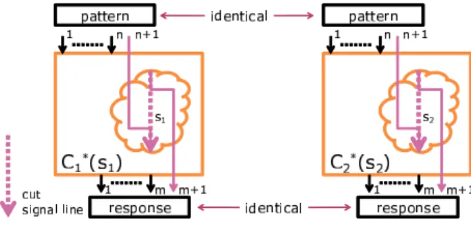
Figure 1. Functionally equivalent signal lines s1and s2.
dence between gate level nets and RTL signal lines estab- lished by the previous signal line mapping methodology. Section 4 discusses the implementation of the signal line mapping proposed in Section 2. Section 5 shows case stud- ies. Section 6 concludes the paper.
2 RTL-GL signal line mapping problem
In this section, we define functional equivalence rela- tion between two signal lines and our target circuits, and also formulate the problem searching functionally equiva- lent nets. Furthermore, we will also show an algorithm for solving the problem.
2.1 Functional equivalence
Here, we first define signal line cutting, which is an op- eration needed for defining functionally equivalent signal lines.
Definition 1: (Signal line cutting) For a combinational cir- cuit C with n inputs, m outputs and an internal signal line s, the following operation is referred to as cutting C on s.
1. Create the(n+1)-th new input port and the (m+1)-th new output port.
2. Remove the signal line s.
3. Create connections between(n + 1)-th input port and the end point of s and between the start point of s and the(m + 1)-th output port.
In the following discussion, we represent the combinational circuit resulting from the above operations as C∗(s).
For two functionally equivalent combinational circuits, we define a functional equivalence of signal lines as fol- lows.
Definition 2: (Functionally equivalent signal line) For two functionally equivalent combinational circuits C1and C2with internal signal lines s1and s2, respectively, s1and
s2 are functionally equivalent if C1∗(s1) and C2∗(s2) are functionally equivalent.
Figure 1 illustrates functionally equivalent signal lines. The signal lines s1and s2are functionally equivalent if the responses from C1∗(s1) and C2∗(s2) are identical for any input pattern. If there is only a limited number of input patterns, then limited functional equivalence can be consid- ered. Let X be a set of patterns with n bits. Let X∗be the
set of patterns with n+ 1 bits formed by expanding each x ∈ X into x&0 and x&1 where ’a&b’ denotes concatena- tion of vectors a and b. The pattern translation from set X to X∗is bit expansion of X.
Definition 3: (Functionally equivalent signal line w.r.t. X) For two n-input combinational circuits C1 and C2 with internal signal lines s1 and s2, respectively, we generate (n + 1)-input combinational circuits C1∗(s1), C2∗(s2) by cutting s1, s2, respectively. Given a set of n bit input patterns, X, and its expanded set X∗, s1 and s2 are functionally equivalent w.r.t. X if any pattern of X∗ is applied to C1∗(s1) and C2∗(s2), their output responses are identical.
Lemma 1 Let C1, C2and s1be functionally equivalent cir- cuits and a signal line in C1, respectively. If there exists at least one signal line that is functionally equivalent to s1in C2 and if there exists only one signal line s2that is func- tionally equivalent to s1w.r.t. a set of input patterns, then s1and s2are functionally equivalent.
[Proof] The set of signal lines in C2 that are function- ally equivalent to s1 in C1 w.r.t. a set of input patterns, X, properly includes all the signals in C2that are function- ally equivalent to s1. Therefore, if there exists functionally equivalent signal lines to s1in C2and s2is only the signal line that is functionally equivalent to s1 w.r.t. X, then s1
and s2are functionally equivalent.
2.2 Circuit model
In this paper, we only consider structural RTL designs. A structural RTL design consists of a controller represented by combinational modules and state registers, and a datapath represented by RTL modules and signal lines connecting them where an RTL module is a MUX or an operational module or a register. An RTL signal line consists of one-bit signal lines as follows.
Definition 4: (Bit-sliced RTL signal line) For an RTL sig- nal line s, each one bit signal line separated from s is re- ferred to as a bit-sliced RTL signal line of s. The i-th bit of s is represented as s[i].
For solving signal line mapping problem, it is sufficient to consider only the RTL combinational circuit CR which is the combinational part of a given structural RTL design SR and the gate level combinational circuit CG which is the combinational part of a gate level design synthesized from SR. We assume that there is a one-to-one correspon- dence between the input/output signal lines of CRand CG. This relation is called I/O mapping information. The I/O mapping information of CR and CG can be obtained by preserving all the bits of the registers in SR during logic synthesis.
2.3 RTL-GL signal line mapping problem
In this subsection, we formulate the RTL-GL signal line mapping problemto find a set of nets, which is functionally
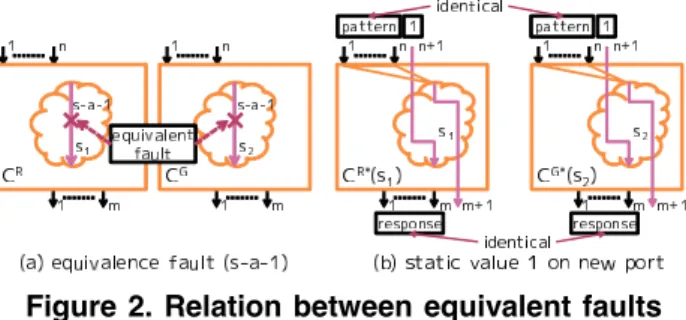
Figure 2. Relation between equivalent faults and functionality of respective signal lines. equivalent to a bit-sliced RTL signal line in an RTL combi- national circuit, in a gate level combinational circuit. Definition 5: (RTL-GL signal line mapping problem) Input
• CR: an RTL combinational circuit design
• CG: a gate level circuit that is functionally equivalent to CR
• The I/O mapping information between CRand CG
• eR[k]: the k-th bit-sliced RTL signal line of an RTL signal line eRin CR
Output EG = !eG|eG≡leR[k]" where eG is a net in CG and ≡lis a symbol representing relation of functional equivalence of signal lines
2.4 Proposed method
Given an RTL combinational circuit CR and a gate level combinational circuit CG, checking functional equiv- alence between a bit-sliced RTL signal line eR in CRand a gate level net eG in CG can be performed by applying all the possible input patterns to both circuits CR∗(eR) and CG∗(eG), and comparing their output responses. For each bit-sliced RTL signal line, by examining every gate level net, we can identify functionally equivalent gate level nets. However, it is not practical to explicitly check all the pos- sible input patterns and the functional equivalence for all the combinations of nets in gate level circuit and bit-sliced RTL signal lines. Ravi et al.[6] proposed a method find- ing candidates for functionally equivalent nets of a given bit-sliced RTL signal line using fault diagnosis techniques using test patterns (i.e., limited input patterns). In this pa- per, their method is utilized to solve the RTL-GL signal line mapping problem. More specifically, their method assumes that the bit-sliced RTL signal line has a stuck-at fault and finds the stuck-at faults, which have the identical behavior of the fault under the test patterns, in the gate level circuit. The faults in the gate level circuit and the fault in the RTL circuit are said to be equivalent. It is a necessary condition for functional equivalence that the responses of the RTL cir- cuit and the gate level circuit are identical when a value v is fixed to eRand eG(see Fig.2 (b)), when s-a-v is assumed to be presented on eGand on eR(see Fig.2 (a)).
Moreover, we propose an algorithm to find a set of func- tionally equivalent gate level nets w.r.t. a set of limited input
patterns of the bit-sliced RTL signal line. Note that the set of the gate level nets obtained by the proposed algorithm may include not functionally equivalent nets.The solution of RTL-GL signal line mapping problem can be used for solving path mapping problem only if the solution does not include not functionally equivalent nets. We show that the algorithm can identify the functionally equivalent net of the bit-sliced RTL signal line under some assumption in The- orem 1. We also evaluate the effectiveness through case studies in Section 5. The algorithm to solve the RTL-GL signal line mapping problem is as follows.
1. Generate a complete test set T for all the testable stuck-at faults in CG.
2. For each v ∈ {0, 1}, the following two steps are per- formed.
(a) Obtain a set of faulty output responses Rf v by applying T to the RTL circuit CR with an in- jected s-a-v fault on the given bit-sliced RTL sig- nal line eR[k].
(b) Find all the single s-a-v faults of CGsuch that all the faulty circuits induced by the faults respond the same output responses Rf v when T is ap- plied to these circuits. Here we refer the faults the equivalent faults. A set of the nets is referred to as EGvsuch that the nets have equivalent faults. 3. Obtain EG= EG0∩EG1.
4. Extract the input cone circuit CR(eR[k]) of the addi- tional primary output appeared by cutting eR[k] where the input cone circuit of a signal line s in a circuit C is referred to as C(s).
5. For each eG ∈ EG, make an input cone circuit CG(eG) of the additional primary output added by cut- ting eG.
6. For each CG(eG), remove eG from EG if the set of the output responses of CR(eR[k]) and CG(eG) are not identical when T is applied.
Steps 1-3 are the same as the procedure for searching functionally equivalent signal line by using fault diagnosis technique in [6]. In [6], the complete test set T for the de- tectable faults in a gate level circuit is used as the fault di- agnosis input patterns. The procedure first finds the s-a-0 (resp. 1) faults in CGthat are equivalent to the s-a-0 (resp. 1) fault injected on eR[k]. Then the procedure selects gate level nets that have both s-a-0 and s-a-1 faults as the equiv- alent faults. Moreover, in this paper, for the set of gate level nets obtained by steps 1-3, we add steps 4-6 to exclude the gate level nets that have different values from the bit-sliced RTL signal line for same pattern of T . Lemma 2 shows that, for a bit-sliced RTL signal line eR[k], the algorithm outputs the functionally equivalent nets of eR[k] w.r.t. a set of input patterns T as a solution to the problem.
Lemma 2 Given an RTL combinational circuit CR, its syn- thesized gate level circuit CG and a bit-sliced RTL signal
line eR[k] in CR. Any eG∈EGare functionally equivalent to eR[k] w.r.t. a set of input pattern T such that EGis the set of gate level nets in CGobtained by the RTL-GL signal line mapping algorithm.
[Proof] The RTL-GL signal line mapping algorithm mainly consists of two steps:
(i) Select gate level nets that have both s-a-0 and s-a-1 faults as the equivalent faults of s-a-0 and s-a-1 on eR[k] under T , respectively.
(ii) For EG obtained by (i), eG ∈ EG is removed if the input cone circuits of eG in CGand eR[k] in CR, re- spectively, are not functionally equivalent.
We show that (i) and (ii) satisfy the condition of Definition 3 where primary outputs of CGand CRhave the same output response when eG and eR[k] have the same value for any input pattern of T .
First, we show that (i) guarantees that the primary out- puts of CG and CR have the same response for any in- put pattern in T when eG and eR[k] have the same value. Let CR has n inputs (xR[i](i = 1, . . . , n)) and m out- puts (zR[i](i = 1, . . . , m)). CR∗(eR[k]) has n + 1 inputs (xR∗[i](i = 1, . . . , n + 1)) and m + 1 outputs (zR∗[i](i = 1, . . . , m + 1)). We inject a s-a-v fault on eR[k] in CR where v ∈{0, 1}. For any t ∈ T , the output response from zR[1], . . . , zR[m] of CRwith the s-a-v obtained by apply- ing t to CRwith the fault and that from zR∗[1], . . . , zR∗[m] of CR∗(eR[k]) obtained by applying t&v to CR∗.
Let CG has n inputs (xG[i](i = 1, . . . , n)) and m out- puts (zG[i](i = 1, . . . , m)). CG∗(eG) has n + 1 inputs (xG∗[i](i = 1, . . . , n + 1)) and m + 1 outputs (zG∗[i](i = 1, . . . , m + 1)). We inject a s-a-v fault on signal line eG in CG. For any t ∈ T , the output response from zG[1], . . . , zG[m] of CG with the s-a-v obtained by apply- ing t to CGwith the fault and that from zG∗[1], . . . , zG∗[m] of CG∗(eG[k]) obtained by applying t&v to CG∗
Consequently, for any input pattern of T , the output re- sponses from zR∗[1], . . . , zR∗[m] and zG∗[1], . . . , zG∗[m] of CR∗(eR[k]) and CG∗(eG), respectively, are the same because CRand CG are functionally equivalent and s-a-v faults on eR[k] and eGare equivalent under T .
Next we show that (ii) guarantees that eG ∈ EG and eR[k] have the same value. For the procedure 4-6, the RTL- GL signal line mapping algorithm excludes all the signal lines having different output responses by applying some input pattern of T . Therefore eG ∈EGand eR[k] have the same value for any input pattern of T .
From the above discussion, every element of EG and eR[k] are functionally equivalent w.r.t. T .
Theorem 1 Given an RTL combinational circuit CR, its synthesized gate level circuit CGand a bit-sliced RTL sig- nal line eR[k] in CR. For the RTL-GL signal line mapping algorithm, eG ∈ EG is the functionally equivalent net in CG of eR[k] if there exists at least one functionally equiv-
alent net of eR[k] and the solution of the algorithm is with
|EG| = 1.
[Proof] From Lemma 2, every eG∈EGobtained by RTL- GL signal line mapping algorithm is functionally equivalent to eR[k] w.r.t. T . Since |EG| = 1, from Lemma 1, the element of EGis functionally equivalent to eR[k].
3 RTL-GL path mapping problem
In this section, we define a gate level path, an RTL path and functional equivalence between them. Furthermore, we formulate the path mapping problem and present a solution of the problem.
3.1 Gate level and RTL path models
Definition 6: (Gate level path) An ordered set of gate level nets{eG1, . . . , eGn} is called a gate level path if the following conditions are satisfied.
(1) eG1 is the net adjacent to a primary input or the output of an FF
(2) eGn is the net adjacent to a primary output or the input of an FF
(3) eGi (i = 2, . . . , n−1) is the net connecting between the gates having eGi−1as an input and eGi+1 as an output, respectively
Definition 7: (Sub gate level path) A subset of a gate level path pGis called a sub gate level path of pG.
Definition 8: (RTL path) An ordered set of RTL signal lines!eR1, . . . , eRn" is called an RTL path if the following conditions are satisfied.
(1) eR1 is the line adjacent to a primary input or the output of a register
(2) eRn is the line adjacent to a primary output or the input of a register
(3) eRi(i = 2, . . . , n − 1) is the signal line connecting be- tween the modules having eRi−1as an input and eRi+1as an output, respectively
Definition 9: (Sub RTL path) A subset of an RTL path pR is called a sub RTL path of pR.
Definition 10: (Bit-sliced RTL path) An ordered set of bit- sliced RTL signal lines!eR1[k1], . . . , eRn[kn]" is called a bit- sliced RTL pathif the following conditions are satisfied.
(1) eR1[k1] is the k1-th bit-sliced RTL signal line adjacent to a primary input or the output of a register
(2) eRn[kn] is the kn-th bit-sliced RTL signal line adjacent to a primary output or the input of a register
(3) eRi[ki](i = 2, . . . , n − 1) is the ki-th bit-sliced RTL signal line connecting between the modules having eRi−1[ki−1] as an input and eRi−1[ki+1] as an output, re- spectively
Definition 11: (Sub bit-sliced RTL path) A subset of a bit- sliced RTL path pR is called a sub bit-sliced RTL path of pR.
3.2 Relation between paths
We define the functional equivalence between sub bit- sliced RTL path and sub gate level path as follows. Definition 12: (Functionally equivalent path) Sub bit- sliced RTL paths and sub gate level paths are simply referred to as sub paths. Sub paths q1 = {e11, . . . , e1n} and q2 = {e21, . . . , e2m} are functionally equivalent if q1
and q2satisfy the following conditions. (1) n= m
(2) e1i ≡le2i (i = 1, . . . , n)
Definition 13: (Identification of path) A sub RTL path qR is said to uniquely identify an RTL path pRif pRis the only path that properly includes qR.
3.3 RTL-GL path mapping problem
We formulate the RTL-GL path mapping problem as a problem to search a set of sub-gate level paths correspond- ing to an RTL path.
Definition 14: (RTL-GL path mapping problem) Input
• CR: an RTL combinational circuit
• CG: a gate level circuit that is functionally equivalent to CR
• The I/O mapping information between CRand CG
• pR: an RTL path Output PG=
n
#
i=0 mi
#
j=0
PijG
Where PijG is defined as follows. Let qiR(i = 1, . . . , n) be a sub RTL path that uniquely identifies pRand qRij(j = 1, . . . , mi) be a sub bit-sliced RTL path of qiR where n is the number of the sub RTL paths of pR. Let qijG be a sub gate level path that is functionally equivalent to qijR. PijGis a set of gate level paths including qijG.
3.4 RTL-GL path mapping algorithm
We propose an algorithm solving the RTL-GL path map- ping problem as follows. The algorithm establishes corre- spondences between an RTL path pRand a set of gate level paths, PG.
(1) Generate the minimum sub RTL path qiR(i = 1, . . . , n) that uniquely identifies pR.
(2) Obtain a gate level net eGijkthat is functionally equiv- alent to each bit-sliced RTL signal line qijRk(k = 1, . . . , l), where qRijkis an element of a bit-sliced RTL path qRij(j = 1, . . . , mi) of qiR, mi is the number of combinations of bit-sliced RTL paths obtained by specifying bit portion of every RTL signal line on qiR, and l is the number of RTL signal lines on qiR. (3) For each pair of i and j, find all the gate level paths
that include!eGij
1, . . . , eGijl". The set of the obtained gate level paths is referred to as PijG.
(4) Calculate PG =
n
#
i=0 mi
#
j=0
PijG.
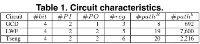
Table 1. Circuit characteristics.
Circuit #bit #P I #P O #reg #pathR #pathb
GCD 4 2 1 3 8 692
LWF 4 2 2 5 19 7,600
Tseng 4 2 2 6 20 2,216
4 Implementation of signal line mapping
In this section, we discuss an implementation of the RTL-GL signal line mapping. Using this implementation, proposed method can be used to map an identified RTL false path by the method in [9] into corresponding gate level paths automatically.
4.1 Searching equivalent fault
In steps 1-3 of the algorithm, we search functionally equivalent nets by using equivalent fault relation. The test pattern set created in step 1 which detects all the detectable faults in CGcan be generated by some ATPG tool. The out- put responses Rf 0(resp. Rf 1) of step 2a can be calculated by some RTL simulation tool for CR with the s-a-0 (resp. s-a-1) fault. For step 2b, we can realize automation by some fault diagnosis tool.
4.2 Checking the values of signal lines
In steps 4-6 of the algorithm, we evaluate that the bit- sliced RTL signal eR[k] and the gate level net eG, which is obtained by the former steps, have the same value for any input pattern of T . This is realized with evaluating if output responses from input cone circuits of eR[k] and eGin CR and CG, respectively, are the same for every pattern of T .
5 Case study
In this section, we show experimental results for evaluat- ing our RTL-GL path mapping method. We used three RTL benchmark circuits, GCD, LWF and Tseng. In this exper- iments, we used only the datapath part of each circuit and tried to map all the paths in the datapath. Table 1 shows the circuit characteristics of the circuits. Columns#bit, #P I,
#P O, #reg, #pathRand#pathbshow the bit width, the number of primary inputs, that of primary outputs, that of registers, that of RTL paths and that of bit-sliced RTL paths. We use the RTL path mapping ratio (P mr) given by P mr= |P
RT|
|PR| ×100[%] as an evaluation criterion. Where
|PR| is the total number of RTL paths in the datapath and
|PRT| is the number of RTL paths mapped. Furthermore, to evaluate more in detail, we consider bit-sliced RTL paths in the datapath. We use the bit-sliced RTL path mapping ratio (P mrb) given by P mrb= |P
RT b |
|PbR| ×100[%]. Where |PbR| is the total number of bit-sliced RTL paths in the datapath and
|PbRT| is the number of bit-sliced RTL paths mapped. Table 2 shows the above path mapping ratio obtained by our proposed method for the three datapaths of the bench- mark circuits. The proposed method achieves the RTL path mapping ratio and the bit-sliced RTL path mapping ratio of average85.9% and 79.1%, respectively. The reason why
Table 2. Path mapping. Circuit GCD LWF Tseng Avg P mr 88.9% 73.7% 95.0% 85.9% P mrb 72.3% 65.7% 99.3% 79.1%
Table 3. Er- ror ratio.
[6] 5.0% ours 0% (bit-sliced) RTL paths which cannot be mapped to gate level paths exist is that the algorithm cannot find any signal line needed for path mapping, i.e., there exist no functionally equivalent net in the gate level circuits.
For the RTL-GL signal line mapping, the proposed method guarantees to get a correct solution provided that there exists at least one gate-level net that is functionally equivalent to a targeted bit-sliced RTL signal line. There- fore, we need to evaluate the impact of the assumption, i.e., the ratio of signal mapping errors induced by the as- sumption to the total number of signal lines to be mapped should be evaluated. The error ratio(Err) is given by Err= |e
Err b |
|eRb| ×100[%]. Where |eRb| is the total number of bit-sliced RTL signal lines in the datapath and|eErrb | is the number of bit-sliced RTL signal lines which are incorrectly mapped to gate level nets. In this paper, we calculate Err for the datapath of LWF. If we use the method of Ravi et al.[6] for the purpose of the signal line mapping, the method more likely to make errors than the proposed method. Table 3 shows the mapping error ratio of the proposed method and that of the method of [6].
Compared to the method of [6], the proposed method guarantees to find nets which are functionally equivalent to a bit-sliced RTL signal line w.r.t. T by employing ad- ditional procedure 4-6. However, time required for the pro- cedure 1-3 dominates the overall execution time. There- fore the proposed method can improve accuracy of the sig- nal line mapping without a large impact on its execution time. Furthermore, even if our method chooses a net which is not functionally equivalent to the bit-sliced RTL signal line(irrespective of T ), it may not directly induce incorrect path mapping. Since, for a bit-sliced RTL path, there are several signal lines must be mapped and the mapped gate level nets must be structurally connected, it is conceivable that the mapping error may be absorbed during path map- ping.
6 Conclusions
Establishing correspondence between an RTL circuit and its synthesized gate level circuit is important for high level testing approaches. In this work, we focus on correspon- dence between a path in the RTL circuit and paths in the gate level circuit. Existence of the correspondence enables the technologies that handle a path at RTL as a bundle of a tremendous number of paths in the gate level circuit. There is a method to identify false paths using RTL design in- formation [9] which is feasible only if RTL paths can be mapped into gate level paths. The method can quickly iden- tify false paths using RTL information under the assumption
that correspondence between RTL paths and gate level paths is available. Until now, it is guaranteed only by a restricted logic synthesis.
In this paper, we propose a method to establish the corre- spondence between RTL paths and gate level paths without using any restricted logic synthesis. In our case study, for several benchmark circuits, average85.9% of the RTL paths was able to be mapped into gate level paths. The signal line mapping, unfortunately, may incorrectly select nets which are not functionally equivalent because of restricting search space. In the study, however, only functionally equivalent net was selected.
In our future work, we improve the accuracy of the sig- nal line mapping. Furthermore, to improve the quantity of mapped paths, signal line mapping from an RTL signal line into multiple gate level nets is dealt with.
Acknowledgments
The authors would like to thank Profs. Michiko Inoue and Tomokazu Yoneda of Nara Institute of Science and Technology for valuable discussion and their cooperation. This work was supported in part by Semiconductor Tech- nology Academic Research Center (STARC) under the Re- search Project and in part by Japan Society for the Promo- tion of Science (JSPS) under Grants-in-Aid for Scientific Research (B) (No. 20300018).
References
[1] K. T. Cheng and H. C. Chen. Classification and identification of nonrobust untestable path delay faults. IEEE Trans. on CAD, 15(8):845–853, Aug. 1996.
[2] N. Ikeda, S. Ohtake, M. Inoue, and H. Fujiwara. RTL false path identification using high level synthesis information. Technical Report 482, Feb. 2008.
[3] S. Kajihara, K. Kinoshita, I. Pomeranz, and S. Reddy. A method for identifying robust dependent and functionally un- sensitizable paths. In International Conf. on VLSI Design, pages 82–87, 1997.
[4] A. Krsti´c, S. T. Chakradhar, and K.-T. T. Cheng. Testable path delay fault cover for sequential circuits. In European Design and Test Conf., pages 220–226, 1996.
[5] M. Nourani and C. A. Papachristou. False path exclusion in delay analysis of RTL structures. IEEE Trans. on Very Large Scale Integration Systems, 10(1):30–43, Feb. 2002.
[6] S. Ravi, I. Ghosh, V. Boppana, and N. K. Jha. Fault-diagnosis- based technique for establishing RTL and gate-level corre- spondences. IEEE Trans. on CAD, 20(12):1414–1425, 2001. [7] S. M. Reddy, S. Kajihara, and I. Pomeranz. An efficient method to identify untestable path delay faults. In Asian test symposium, pages 233–238, 2001.
[8] R. Tekumalla and P. Menon. Identifying redundant path de- lay faults in sequential circuits. In International Conf. VLSI Design, pages 406–411, 1996.
[9] Y. Yoshikawa, S. Ohtake, and H. Fujiwara. False path iden- tification using RTL information and its application to over- testing reduction for delay faults. In Asian Test Symposium, pages 65–68, 2007.