Power-Aware Multi-frequency Heterogeneous SoC Test Framework Design with
Floor-Ceiling Packing
Dan Zhao and Ronghua Huang The Center for Advanced Computer Studies
University of Louisiana at Lafayette Email: [email protected]
Tomokazu Yoneda and Hideo Fujiwara Graduate School of Information Science Nara Institute of Science and Technology
Email: [email protected]
Abstract— This paper presents a solution to the multi-frequency het- erogeneous SoC test integration and reuse, which is considered the major hurdle of SoC manufacturing capability, and thus is the key component of SoC test automation. A hybrid system level test framework is designed and optimized to tackle heterogeneous test environment with the combination of BIST and the external test. Several interdependent design items including test access mechanism routing, bandwidth matching, multi-frequency interface configuration, and test scheduling under tight power and pin count limitation, are well studies and incorporated into the test framework. The trade-off between test time, test power and bandwidth is well balanced to achieve the minimum test cost in terms of test time and test interface. The simulation study shows the promising results of the proposed floor-ceiling packing approach1.
I. INTRODUCTION
Spurred by the technology leading to millions of transistor integra- tion, System-on-Chip (SoC) has evolved as a new design paradigm, allowing an entire system built on a single silicon. An SoC embeds a large number of complex, heterogeneous components known as IP (intelligent property) cores operating at different frequencies. In consequence, the test of SoC has become an enabling technology for the SoC design paradigm to bridge the widening gap between design capability and manufacturing capability. The cost of testing a transistor will even reach or overtake the cost of manufacturing a transistor by 2010 [1]. While the ever increasing complexity and heterogenity of cores has driven the new urgency for SoC test, the IP reuse in SoC design has complicated everything. Integrating a verity of IP cores drawn from different sources, each with its own test strategy and test implementation, the system designer is confronted with the challenge of developing a new SoC test framework that stitches together various test structures for IP cores into a coherent one and minimizes test cost in terms of test time and test interface. Our earlier work has been concentrated on the single-frequency wrapper/TAM cooptimization and test scheduling [2], [3]. Recently, we have proposed multi-frequency wrapper architectures and test cost reduction techniques for single-core designs [4], [5]. In this paper, we will propose an embedded SoC test framework that integrates core- level test logics, a test access architecture, and a mixed test structure at chip-level. To the best of our knowledge, this is the first paper to present a multi-frequency SoC test framework for heterogeneous test environment. The rest of the paper is organized as follows. In Sec. II, we discuss the background and the motivation of multi-frequency heterogeneous SoC test. Then in Sec. III, we formulate the problem into 2−D bin packing and propose an efficient heuristic algorithm to design and optimize the test framework with resource partitioning and test scheduling to minimize test cost. The performance of the proposed approach is evaluated in Sec. IV, and finally we conclude the paper.
1This research is supported in part by LA BORSF Research Competitive Subprogram, and Japan Society for Promotion of Science (JSPS) under grant S06089.
II. RATIONALE
We assume a comprehensive test environment where each individ- ual core is testable by either a built-in self-test (BIST) or an external test such as scan test or a combination of them to achieve high fault coverage. We also assume that each core contains one or several scan paths. Deeply embedded in a SoC, the cores are not directly accessible from chip I/O pins. A bus-based test access mechanism (TAM) is thus constructed for scannable cores to transport test stimuli from the external ATE to the core-under-test (CUT) or test responses from CUT to ATE. ScanBIST scheme is used for BISTed cores where the BIST engine is logically divided into the Test Pattern Generator (TPG) and Test Response Evaluator (TRE). A single BIST engine can be used to test one or multiple BISTed cores which are located near to the BIST engine. To ensure core access and isolation necessary for test independence, each core is surrounded by a test wrapper such as IEEE Std. 1500 wrapper. It switches between different modes, i.e., internal test mode, external test mode, and normal function mode, according to the control signals received.
Test resource partitioning and distribution cover various aspects, such as the sharing of test sources and sinks including external ATE and on-chip BIST engines, the routing of TAMs, the design of multi-frequency test interface, the configuration of wrapper scan architecture, the partitioning of test pins, and the distribution of band- width and power budget. Thus, a system level optimization technique need to be developed to ease test integration, to facilitate concurrent testing, and to efficiently partition the test resources while alleviating the impact of expensive state-of-the-art SoC test equipment. In this work, we will develop such an integrated framework that facilitates reusability and flexibility from all design aspects.
III. PROPOSEDAPPROACH
A. Design of Multi-Frequency Interface
Most of prior research assumes that the cores are clocked at ATE frequency ft during testing. It turns out that there is a mismatch between the ATE capability and core test speed [6]. Using sub- frequencies derived from a high-speed on-chip clock improves test efficiency from two aspects. On one hand, it can save power dissi- pation when setting core test clock rate lower than the ATE. On the other hand, it can reduce the test time by running at higher clock rate. We will achieve the best tradeoff between them by designing a multi- frequency interface that synchronizes the input data and transfers test patterns into the corresponding scannable core. During scan testing, the test data is transported from/to the ATE along the parallel TAMs with width of Wextand frequency of ft. The bandwidth Wext× ft
is distributed to the cores at distinct frequency via pairs of MUX- DeMUXmulti-frequency interface. The dedicated TAM width for a core Ciis determined by witam=wcif×fci
t . The TAM design should be constrained by the pin count, i.e., Σi = 1Ncwitam≤ Wext. If fci
2007 IEEE International Symposium on Circuits and Systems (ISCAS 2007), pp.2942-2945, May, 2007.
for core Ci is higher than ft, we insert a MUX between the TAM and the core input terminals, and multiplex⌈ffcit⌉ × wci bits test data at ft into core Ciwith wci bits test data at fci. If fci for core Ciis lower than ft, we insert a DeMUX instead, and de-multiplex witam
bits test data at ftinto core Ciwith witam×⌊fft
ci⌋ bits test data at fci. To observe test responses, we will insert DeMUX/MUX accordingly between the core output terminals and the TAM. The design of multi- frequency interface, in which both the width and running frequency assigned to each core are cooptimized, will be incorporated into the framework design to facilitate SoC test cost reduction.
B. Wrapper Configuration with Rectangle Transformation
Core wrapper scan architecture is configured to minimize the test time by constructing wrapper scan chains in a way that their length are well balanced as the longest wrapper scan chain dominates the test time. The wrapper scan width wci of a scan test core Ci is adapted to the TAM width by serially connecting core inputs/outputs with internal scan chains. In order to balance the wrapper scan chains so as to minimize the longest wrapper scan chain length Limax, a best- fit decreasing fast heuristic is applied to solve it. We thus obtain a finite rectangle set Ri(wij, cij) with wij as its jth wrapper scan width and cij as its corresponding clock cycle time for core Ci, which forms the wrapper configuration candidate set. The candidate rectangle set of core Ci provides an important feature of rectangle transformation which facilitates scheduling in an efficient way that the most suitable rectangle will be selected to fit into the available idle space. By incorporating shifting frequency fci, the time of core ci is determined by ti = fcij
ci which is not only dependent on the wrapper scan chain width but also on the shift frequency. Started with this initialization step, we obtain a set of candidate rectangles for each scan test, which provides the flexibility to make the trade-off between wrapper scan width wij and the shift frequency fci, thus results in the best configuration possible by the two dimensions of a rectangle test.
C. Floor-Ceiling Packing to Framework Design
The power-conscious multi-frequency SoC test framework design problem (namely, PMD) is stated as follows. Given an SoC model S, a chip level TAM with Wext limited by the chip pin count, the ATE frequency ft, and the maximum power allowance Pave, determine a chip level TAM design that routes parallel scannable cores, determine the multi-frequency interface for each particular core to match the bandwidth and configure accordingly the wrapper scan architecture, and schedule both scan and BIST test sets in parallel such that the overall test time is minimized while resolving various resource conflicts and satisfying power constraint at any time.
a) Problem Formulation: We formulate the PMD problem into a 2−D bin packing problem. The test set for a core is defined as a rectangle Ti (ti, pi) with the height of test time ti obtained at width of wij and running frequency of fci, and the length of test power pi at fci. The rectangle tests are placed into a 2−D bin in a way that divides the bin into several horizontal shelves and the certain transformation of rectangle test sets are allocated in parallel into shelves. A shelf Sjis bounded by the bottom edge denoted as the floor and the top edge denoted as the ceiling of Sj. The height of shelf Sj, H(Sj), is defined by the height (in time dimension) of the tallest rectangle test fitted into the shelf. The power dissipation for Sj, given by P(Sj) = ΣNi=1c pi× xij (xij= 1 if Tiis located in shelf Sj, 0 otherwise.), should satisfy the power constraints, P(Sj) ≤ Pave. The TAM width for Sj, given by W(Sj) = Σi=1Ncwtami × xij, should match the ATE bandwidth, W(Sj) ≤ Wext. Since the cores
within distinct shelves are tested in sequential, the height of the bin, ΣNj=1H(Sj) is the overall test time for SoC S.
Hence, the PMD problem is deduced to minimizing the height (TSoC) of the bin while meeting the length of Pave or Wext
limitation. The proposed approach can be divided into three major steps, namely, floor packing of scan tests, ceiling packing of BIST tests (in existing shelves), floor-ceiling packing of remaining BIST tests (by creating new shelves). In this section, we give an intuitive description of each step and illustrate the approach with the pseudo- code.
b) Step I: Floor Packing of Scan Tests: We first allocate scan testable cores on parallel routing TAMs to utilize the top level TAM width to the maximum extent. The multi-frequency interface and wrapper scan architecture for each core is determined accordingly during the scheduling of scan tests. An efficient floor packing approach is proposed here for constrained scheduling. Assuming a 2- D bin with its length bounded by Pave. We allocate the rectangles of test sets in a way that divide the bin into several horizontal shelves. The basic idea is that a rectangle scan test is packed left on floor justified on the first shelf where it fits. If no shelf can contain it, a new shelf is created and the rectangle is packed left into the shelf. Step I: Floor Packing of Scan Tests
1:order(Lc= {Ci|i ∈ 1...Nc}); 2:N :=0;
3:U nscheduled:= {Lc}; 4:while(|U nscheduled| ̸= 0)
5: N ++;
6: SN:= {∅};
7: find Cmax:= maxi∈U nscheduled{ti}; 8: SN:= SN!{Cmax};
9: U nscheduled:= U nscheduled\{Cmax}; 10: H(SN) := tCmax;
11: compute idle P ow & idle BW ; 12: Cskip= {∅};
13: while(|Cskip| ̸= |U nscheduled|) 14: find Ctmp= maxi∈U nscheduled{ti}; 15: compute maximum possible fsCtmp & related
wCtmp from idle P ow & idle BW ; 16: if (tCtmp≤ H(SN))
17: SN := SN
!{Ctmp};
18: U nscheduled:= U nscheduled\{Ctmp}; 19: find least possible wCtmp such that
tCtmp closest to H(SN); 20: update idle P ow & idle BW ;
21: else
22: Cskip:= Cskip!{Ctmp};
A list of descending ordered tests is used to initiate shelf division. The cores are ordered at their minimum possible test time given the entire TAM width Wext and the whole power budget Pave. We hope that the resources can be released earlier by scheduling the critical ones earlier and more efficiently utilized by smaller cores. Assuming maximum allowable frequency Fmaxi of a core, each core may have a distinct shift frequency for scan test generated by clock division block. In order to simplify the hardware implementation, the ratio of trial frequencies is set as two’s exponent, i.e., ffsk
sk+1 = 2.
We try to find the maximum possible shift frequency fci of core
Ci from a set of trial frequencies at which the shift operation is performed without exceeding the power constraint. Then we find the corresponding wrapper design which satisfies the external bandwidth
limit while resulting in the minimum testing time tiat the maximum possible fci. In order to handle the restricted power budget, we try to halve the shift frequency at the same time to increase the wrapper width in a way that won’t result in an increase in test time.
Following the order in LC, we start packing from the highest rectangles. The bin is divided into shelves by the largest rectangle in each shelf. After allocating the highest rectangle test in an empty shelf SN, the height of the shelf is determined by the test time of this core (H(SN) = tCmax). We try to pack in the same shelf the next highest possible unscheduled rectangle Ctmpto use up the remaining TAM width idle BW and power idle P ow. A fast checking process is pursued to find out if a test can be contained in the shelf or not. The power constraint is checked first. A new incoming test can be allocated in the shelf only if its test power obtained at the minimum frequency satisfies the power constraint. When satisfying power constraint, we further check if Ctmp can meet the height allowance at the maximum possible frequency. It can be contained unless its minimum test time does not exceed the shelf height. After passing the check process, the best combination of frequency and TAM width will be picked such that the resulted test time is closest to the shelf height. The reason is simply to free up more bandwidth and power so as to contain more smaller cores next.
c) Step II: Ceiling packing of BIST Tests in Existing Shelves: After packing the scan tests from left to right with their bottom edges on the shelf floor, we start to pack in this step the BIST tests from right to left with their top edges on the shelf ceiling to utilize the idle space. Several constraints should be taken into consideration during the scheduling. First, the resource conflicts between cores, arising from the sharing of BIST engines to test different cores or sharing of the same core to perform both scan test and BIST, should be avoided. Second, the overall power dissipation should meet power budget at any time. Test preemption is employed to favor the BIST scheduling the flexibility to fit into the idle space. Preempting BIST test however requires that the BIST engine to save both the pattern generator and signature analyzer states. It is desirable to keep preemption to a minimum, we thereby define a preemption control parameter to dynamically determine the number of preemptions per test. With preemption, we dynamically divide the BIST test set to best fit into the idle space. In addition, we assume that the BIST tests are running at-speed at distinct functional clock rate.
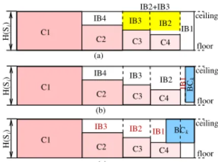
Similarly, we sort the BIST tests in decreasing order of their test time, LBC = {BCi|i ∈ 1...Nc}. In order to efficiently utilize the idle space of each shelf, we construct idle bins IB[1...Nib] in each shelf from right to left as shown in figure 1 (a). The hight and length of each idle bin is determined by the size of the associated scan test under the bin. More specifically, if there is idle power (idle P ow > 0), the first idle bin is initiated with the hight equivalent to the shelf height and the length of the idle power. Otherwise, all idle bins will be created in a way that their height is determined by H(IBj) = H(Si) − tck and W(IBj) = pck(where tckand pckis the scan test time and scan test power of core Ckrespectively). In order to best fit the BIST test into these idle bins, we consider the combinations of idle bins in the order of{IB1}, {IB2+ IB1}, {IB3+ IB2+ IB1}, ...,{IBNib+ IBNib−1+ ... + IB1}. Accordingly, the hight and the length of each combination of multiple idle bins are determined by the smallest height of the idle bin in this group, and the sum of the length of all idle bins in the group, respectively.
We start scheduling the BIST tests in the sequence of all groups of idle bins. The tests are tried to fit into the idle bins based on the order in LBC. Specially, we pick the first group of idle bins, and search through the core list to find the best BIST test that can utilize
floor C2 C3
IB2+IB3 IB1
(c) (b) (a) IB4 IB3
IB2
C2
C4
C1
C3
ceiling C2
C1
IB1
C4 IB4 IB3 IB2 ceiling
floor C3
floor ceiling
C1
IB2 IB1 IB3
C4
iH(S ) kBC
iH(S )
BCk
iH(S )
Fig. 1. Allocating and updating the idle bins in each shelf. the idle bin to the maximum extent. If a suitable test is found, the test is allocated, otherwise, a new search of tests is initiated to best fit the next group of idle bins. If a complete test is allocated, it will be marked as scheduled and removed from the list. If only a subset is allocated, the BIST test time of this core is updated and the core list is resorted to ensure that current largest test always has the highest priority to be scheduled. With preemption, we have the flexibility to divide a BIST test dynamically according to the idle space. After a test is allocated, we will update the list of idle bins in two cases.
• In case 1, after a new test CBiis allocated into{IB1}, IB1 is updated with its length shortened into W(IB1) = W (IB1) − pCBk as shown in Figure 1(b).
• In case 2, after a new test CBiis allocated into a combination of idle bins, some bins are eliminated while the remaining are updated. For example as shown in Figure 1(c), the previous IB1 is eliminated while IB2 is updated to IB1 with its length of W(IB1) = W (IB1) + W (IB2) − pCBk.
We will repeat the above process for each shelf until all BIST tests have been scheduled thus we finish the entire scheduling or all existing shelves have been packed and we will move on the third step.
Step II: Ceiling Packing of BIST Cores 1:order(LBC= {BCi|i ∈ 1...Nc}); 2:BC[1..Nc].sched=False;
3:num sched=0; 4:for (i:=1 to N )
5: construct idle bins IB[1...Nib]; 6: while(shelfdone==False) 7: Unscheduled:={LBC}; 8: for (k:=1 to Nib)
9: calculate comtime & compower; 10: for (j:=1 to Nc)
11: choose the best-fit test BCi∈ Unscheduled that not conflicting with scan tests, and pBCi ≤ compower, and allowing preemption; 12: recalculate tBCi;
13: if (BCi is finished)
14: BCi.sched=True;
15: num sched ++;
16: update LBC;
17: update idle bins;
18: break;
19: if (no idle bins exist or no cores can fit) 20: shelfdone=Ture;
21: if (num sched==Nc) 22: break;
d) Step III: Floor-Ceiling Packing of Remaining BIST Tests: In the last step we apply floor-ceiling packing to the remaining
TABLE I
COMPARISON OF THE TOTAL TEST TIME OFSOCD281WITH PREEMPTIVE TESTING.
Wext Pave= 1000 Pave= 1500 Pave= 2000
Case1 Case2 Case3 Case4 Case1 Case2 Case3 Case4 Case1 Case2 Case3 Case4
8 351.365 328.005 199.055 185.125 329.285 328.005 175.145 166.135 328.005 328.005 166.365 166.135 16 199.055 185.125 136.93 110.5 183.975 166.135 113.99 88.84 166.365 166.135 98.63 85.48 24 157.475 123.435 125.5 86.61 132.435 110.835 97.645 73.45 114.175 110.835 83.11 65.78
32 136.93 110.5 119.46 84.4 113.99 88.84 97.645 63.965 98.63 85.48 75.985 57.655
40 132.25 90.1 119.46 80.9 99.77 76.7 83.56 57.89 95.29 67.87 71.17 54.855
48 125.5 84.4 119.46 78.705 97.645 73.45 77.39 57.885 83.11 65.78 62.28 52.48
56 119.46 81.555 119.46 73.36 85.93 69.175 77.39 56.25 78.835 60.045 62.28 52.48
64 119.46 78.705 119.46 67.17 79.57 63.965 76.6 55.55 78.685 57.655 61.33 49.21
TABLE II
COMPARISON OF THE TOTAL TEST TIME OFSOCD281WITH NON-PREEMPTIVE TESTING.
Wext Pave= 1000 Pave= 1500 Pave= 2000
Case1 Case2 Case3 Case4 Case1 Case2 Case3 Case4 Case1 Case2 Case3 Case4
8 353.695 328.005 199.055 186.845 329.285 328.005 187.655 166.135 328.005 328.005 166.365 166.135 16 199.055 186.845 140.735 111.32 187.655 166.135 123.37 109.32 166.365 166.135 111.32 105.96 24 157.475 131.435 136.93 106.425 137.795 131.315 104.79 93.01 131.825 131.315 99.23 90.99 32 140.735 111.32 126.65 104.05 123.37 109.32 97.665 83.865 111.32 105.96 92.355 79.695
40 136.93 100.4 126.65 99.93 106.14 96.7 97.21 76.275 99.79 90.99 85.945 70.585
48 133.67 99.23 126.65 99.23 104.79 93.01 84.045 72.16 99.23 88.35 83.57 68.21
56 126.65 95.205 126.65 96.77 100.515 87.745 83.98 71.97 95.205 84.345 79.45 68.21
64 126.65 92.355 126.65 92.355 97.665 83.865 83.57 68.21 92.355 79.695 76.29 58.32
unscheduled BIST tests by creating new shelves. Again, the BIST tests are sorted and the one with larger test time will be considered earlier. For each new shelf, the largest BIST test packed into the shelf determines its height. Floor packing is applied first and then follows the ceiling packing until no test can be fit into this shelf. The resulted final height of the bin is the overall test time of the SoC.
IV. SIMULATIONSTUDY
We evaluate the proposed PMD algorithm by running simulations on a ITC’02 SoC test benchmark d281 which provides a combination of scan and BIST test patterns. This example SoC model contains eight cores running at different clock frequencies. For each core, a set of test parameters are provided, including the functional clock domain, the number of inputs, outputs and bidirectional terminals, the average power consumption when shifting at 100 M Hz, the number of scan chains and their length. We compare the overall test time for d281 under four cases.
• Case 1: The ATE frequency ft=100MHz and maximum trial frequency for a core Fmax=100MHz.
• Case 2: The ATE frequency ft=100MHz and maximum trial frequency for a core Fmax=200MHz.
• Case 3: The ATE frequency ft=200MHz and maximum trial frequency for a core Fmax=100MHz.
• Case 4: The ATE frequency ft=200MHz and maximum trial frequency for a core Fmax=200MHz.
We run experiments with the top level TAM width Wext changing from 8 to 64 while the power limit Pave at 1000, 1500 and 2000 respectively. The simulation results are listed in Tables I, II.
When comparing the results, we can see that for the same ATE fre- quency and a given external TAM width (i.e., the external bandwidth limit is fixed at BWext= Wext× ft), their corresponding test time is reduced further when the trial frequency is increased. It is because the cores can be pulsed at higher frequency to further reduce the scan time if the power constraint allows. While for the same range of trial frequencies≤ Fmax, increasing ftfrom 100M Hz to 200M Hz, the reduction in test time corresponding to a given Wextis also observed. It is due to the fact that the increase in bandwidth limit looses
the design space to tradeoff between shifting frequency and scan time. Moreover, under the same experiment condition, preemptive testing results in further reduction of test time compared to the non-preemptive testing. In this experiment, we set the maximum preemption time to 3 to control the design complexity.
V. CONCLUSION
We have proposed an efficient floor-ceiling packing algorithm to integrate and optimize a multi-frequency heterogeneous SoC test framework under complicated test environment. Such a framework design aims to maximize and simplify SoC test reuse, and provide the system integrator the highest flexibility in planning the overall SoC test strategy. A combination of BIST and scan test structure is embedded to achieve high fault coverage. The reusability and flexibility of the designed framework are reflected in terms of a verity of test structures integrated and optimized based on the trade-off between routing, resource distribution, test time, and test power; ef- ficient scheduling mechanism; and uniform test access methodology.
REFERENCES
[1] P. Gelsinger, “Discontinuities driven by a billion connected machines,” IEEE Design & Test of Computers, vol. 17, no. 1, pp. 7–15, January- March 2000.
[2] D. Zhao and S. Upadhyaya, “Dynamically partitioning test scheduling with adaptive TAM configuration for power-constrained soc testing,” IEEE Trans. on Computer-Aided Design of Integrated Circuits and Systems, vol. 24, no. 6, June 2005.
[3] ——, “A generic resource distribution and test scheduling scheme for embedded core based SoCs,” IEEE Trans. on Instrumentation and Mea- surement, vol. 53, no. 2, April 2004.
[4] D. Zhao, U. Chandran, and H. Fujiwara, “Design and optimization of a power-aware multi-frequency wrapper architecture for modular ip cores,” in IEEE Asia and South Pacific Design Automation Conference, January 2007, to appear.
[5] T. E. Yu, T. Yoneda, D. Zhao, and H. Fujiwara, “Designing power-aware wrapper for multi-clock domain cores using clock domain partitioning,” in IEEE International Workshop on RTL and High Level Testing, November 2006, to appear.
[6] A. Khoche, “Test resource partitioning for scan architecture using band- width matching,” in Digest of Int’l Workshop on Test Resource Partition- ing, 2001, pp. 1.4.1–1.4.8.