Gap plasmon excitation in plasmonic waveguide using Si waveguide
Koji Okuda, Shun kamada, Toshihiro Okamoto, and Masanobu Haraguchi
Department of Optical Science and Technology, Faculty of Engineering, Tokushima University, Minamijosanjima 2-1, Tokushima 770-8506, Japan
E-mail: [email protected]
Plasmonic waveguides have attracted considerable attention for application in highly integrated optical circuits since they can confine light to areas smaller than the diffraction limit. In this context, in order to realize a highly integrated optical circuit, we fabricate and evaluate the optical characteristics of a polymethylmethacrylate junction positioned between Si and plasmonic waveguides. For the plasmonic waveguide, we employ a gap plasmonic waveguide in which the energy of the plasmonic wave can be confined in order to reduce the scattering loss at the junction. By experimental measurement, we determine the coupling efficiency between the Si and gap plasmonic waveguides and the propagating length at the gap plasmonic waveguide to be 52.4% and 11.1 µm, respectively. These values agree with those obtained by the three-dimensional finite-difference time-domain simulation.
We believe that our findings can significantly contribute to the development of highly integrated optical circuits.
1. Introduction
Plasmonic waveguides support propagating surface plasmon polariton modes and confine light energy to areas smaller than the diffraction limit of light1-3. Consequently, plasmonic waveguides are considered as a key component in highly integrated optical circuits and nanosized photonic devices4,5. Such plasmonic waveguide structures include nanorods3,6, metal stripes7,8, gaps9-12 ,wedges13,14, V-grooves15-17, etc. For the realization of highly integrated optical circuits, the combination of a Si waveguide18 and plasmonic waveguide may be suitable; the former and latter are suitable for long-distance optical transmission and light energy injection into nanosized optical devices with super focusing19-22, respectively. The functioning of the combined Si and gap plasmonic waveguides23-25, referred to as the dielectric-loaded surface plasmon polariton (DL-SPP)26,27 waveguide, has been previously demonstrated. However, the scattering loss at the curved section of the waveguide and coupling loss between the Si and plasmonic waveguides is very large.
The first and second modes can exist for a gap plasmonic waveguide with sufficient height9; the first mode propagates along the waveguide edge and the second mode
propagates inside the gap, i.e., the waveguide center. Therefore, the second mode is
expected to exhibit high transmittance and small scattering loss through structures with 90° bends without the need for curvature28,29, because this mode is confined within the gap structure.
In a previous demonstration by Tian et al.23, the gap plasmonic waveguide was reported to only support the first mode. Subsequantly, they concluded that the scattering loss at the junction between the Si and plasmonic waveguides must be larger than that for the waveguide in which the second mode plasmon propagates based on the following
reasoning: it is easy to couple the bulk wave mode as the first mode because the first mode is sensitive to the condition of the metal surface in terms of the surface field distribution.
In the above context, in this study, we employ a gap plasmonic waveguide9 with sufficient height and fabricate a junction structure between Si and plasmonic waveguides. We
perform experiments on our waveguide structure to evaluate the optical characteristics, i.e., coupling efficiency and propagation length of the gap plasmonic waveguide. Subsequently, we demonstrate that gap plasmonic waveguides that can support the second mode are more suitable to construct Si-plasmonic hybrid optical circuits, in comparison with gap
plasmonic waveguides which support only the first mode.
2. Fabrication method, measurement and calculation 2.1 Fabrication of waveguides structure
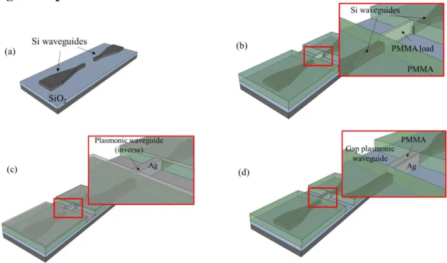
Figure 1 depicts the fabrication process of the Si and gap plasmonic waveguides. First, a spin-coated silicon-on-insulator (SOI) substrate (ZEP-520A, Zeon Corp.) was exposed to an electron beam (EB) directed as per the Si waveguide pattern.
After sputter deposition of Ni, the resist was lifted off, and Si and SiOx etching were
performed with the use of CF4 and Ar gas via reactive ion etching. Next a Si waveguide
structure with a height of 500 nm was fabricated after removing the Ni mask. Further, polymethylmethacrylate (PMMA) was spin-coated on the substrate and exposed to an EB in order to fabricate the gap plasmonic waveguide’s core, which was a dielectric load with a height of 1.2 µm (PMMA load); here, we remark that the second mode in the gap
plasmonic waveguide can be suitably excited with a gap structure height of 1.2 µm. After EB lithography, Ag film was thermally deposited twice at a tilt of 45° to cover the PMMA load, which led to the eventual formation of Ag film with a height of 300 nm height. After Ag deposition, the deposited Ag film on the PMMA load at the top surface of the substrate was removed by means of Ar- ion milling. Subsequent to Ar-ion milling, the fabricated gap plasmonic waveguide with the PMMA core was sandwiched by the Ag film.
2.2 Optical measurement / Simulation
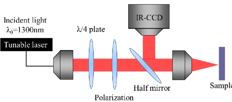
Figure 2 shows our optical measurement set-up to observe scattering light from the waveguide structures. When a polarized laser beam with a vacuum wavelength of 1300 nm was focused onto the input port of the Si waveguide, the light at the output port of the Si waveguide was observed with an IR-CCD camera.
Figure 3 shows the numerical three-dimensional finite-difference time domain (3D-FDTD) model, wherein Figs. 3-(a) and (b) show the Si waveguide model and junction structure, respectively. As mentioned previously, the light source is a laser beam with a vacuum wavelength of 1300 nm. To evaluate the coupling efficiency between the Si waveguide and gap plasmonic waveguide, we calculate the Poynting vector magnitudes at observation planes 1 and 2. Observation plane 1 is set at a distance of 4.4 µm from the light source in the
Si waveguides, as shown in Fig. 3-(b).
Observation plane 2 is set at a distance of 0.45 µm from the end of the plasmonic waveguide, as shown in Fig. 3-(e). In the simulations, we set the dielectric constants of Ag, Si, SiO2, and
PMMA as -71.8+5.23i, 3.45, 1.45, and 1.49, respectively. The widths and heights of the Si and gap plasmonic waveguides were 0.4 µm, and 0.5 µm, and 0.2µm and 1.2 µm, respectively.
3. Results and discussion
Figure 4 shows the scanning electron microscopy (SEM) images of the junction, gap plasmonic waveguide, and Si waveguide structures. Figure 4-(a) shows a bird’s eye view of the SEM image of the junction structure while Fig. 4-(b) shows the cross-sectional view of the junction of the gap plasmonic and Si waveguides. Each waveguide appears as a directly bonded structure. Figures 4-(c) and (d) show the cross-sectional view of the gap plasmonic waveguide with width of 200 nm and height of 1200 nm and the Si waveguide with width of 400 nm and height of 850 nm, respectively. It is to be noted that the image in Fig. 4-(a) was acquired before covering the PMMA layer.
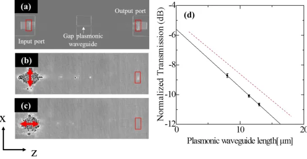
Figure 5-(a) shows the SEM image of the junction structure, while Figs. 5-(b) and (c), show the IR-CCD camera images obtained when X-polarized and Z-polarized light beams were incident on the input port, respectively. From Figs. 5(b) and (c), we observe that scattered light is obtained from the output port only for the X-polarized laser illumination.
Considering the polarization selection for the gap plasmon mode, in Fig. 5-(b), the waveguide mode in the Si waveguide is transformed into the gap plasmon mode in the plasmonic waveguide and re-converted to the waveguide mode in the second section of the Si waveguide; consequently, scattered light appears at the output port. On the other hand, as shown in Fig. 5(c), for Z-polarized laser illumination at the input port, there is no scattered light at the output port. This is because Z-polarized laser light cannot excite the gap plasmon mode in the plasmonic waveguide.
Figure. 5-(d) depicts the scattered light intensities evaluated from the CCD images as a function of the plasmonic waveguide length (filled circles). It is to be noted that the output intensity here is normalized by the intensity at the output port without the gap plasmonic waveguide. The dashed line in the figure represents the numerical intensity calculated via
3D-FDTD with the configuration shown in Fig. 3. The solid line indicates the best-fit curve of the scattering light intensity Is corresponding to the expression
𝐼𝑠 = 𝜂2𝐼
0𝑒−𝑧/𝐿 (1),
where η, I0 and L represent the coupling efficiency, the input light intensity in the Si
waveguide and propagation length, respectively, of the gap plasmonic structure.
From Fig. 5-(d), we note that the experimental results are consistent with the best-fit line. This result indicates that the junction and waveguide structures fabricated in this study are nearly defect-free. In this context, we remark that the fabrication process employed here is simpler than the focused ion beam (FIB) milling technique used to form metal gaps for gap plasmonic waveguides. Further, our approach ensures that the gap sharp as guaranteed by the shape of the PMMA fin as shown in Fig. 4-(c).
From the best-fit of Eq. (1) to the experimental data, we obtained the coupling efficiency between the Si and gap plasmonic waveguides and the propagation length of the gap plasmonic waveguide to be 52.4% (-2.8 dB) and 11.1 µm, respectively. As regards the 3D-FDTD simulation, the coupling efficiency between the Si and Gap plasmonic waveguides and the optical propagating length were determined to be 56% (-2.5 dB) and 12.1 µm, respectively. This value of the propagation length of the plasmonic waveguide in the experiment is close to that of a previously studied metal-insulator-metal (MIM) waveguide slab (16.5 µm) 5, which was calculated with a gap width of 200 nm, and ε
Ag = -71.8 + 5.23i.
The experimental and simulation results thus exhibit a close agreement. This agreement also supports our speculation that the junction and waveguide structures were defect-free. In comparison with previous reports23, the coupling efficiency between the waveguides in this study improved by a factor of 1.7, considering that our junction was not the optimal structure for this configuration. This indicates that the coupling efficiency can be improved by optimizing our waveguide structure30.
In order to achieve an efficient excitation of a guided mode in a waveguide by other guided mode in another waveguide at the junction between two waveguides, the mode-mismatch between modes should be minimized31. The overlap integral between the field distributions
of two modes will allow an estimate of the best coupling. The first and the second modes in the plasmonic waveguide are bounded at the edge and the center in the gap of the waveguide, respectively9. The overlap integral between the second mode in the Gap plasmon waveguide
and the mode in the Si waveguide is larger than that for the plasmonic mode in the plasmonic waveguide in literatures23, considering the field distributions of modes in our plasmonic and Si waveguides for our structure.
In summary, we believe that our findings can significantly contribute to the further development of gap plasmonic waveguides.
4. Conclusions
In this study, we determined the optical characteristics of a PMMA junction positioned between Si and a gap plasmonic waveguides. The coupling efficiency between the Si and gap plasmonic waveguides and the optimal propagating length of the plasmonic waveguide were determined to be 52.4% and 11.1 µm, respectively.
These values agree closely with the corresponding values obtained via 3D simulations. This close agreement between the experimental and simulation results indicates the defect-free nature of our proposed waveguide. We believe that our findings can significantly contribute to improving gap plasmonic waveguide performance.
References
1) J. R. Krenn, Nat. Mater. 2, 210 (2003).
2) S. A. Maier, P. G. Kik, H. A. Atwater, S. Meltzer, E. Harel, B. E. Koel, and A. A. G. Requicha, Nat. Mater. 2, 229 (2003).
3) J. Takahara, S. Yamagishi, H. Taki, A. Morimoto, and T. Kobayashi, Opt. Lett. 22, 475 (1997).
4) D. K. Gramotnev and S. I. Bozhevolnyi, Nat. Photo. 4, 83 (2010).
5) S. I. Bozhevolnyi, Plasmonic Nanoguides and Circuits (Pan Stanford Publishing, 2009). 6) T. Onuki, Y. Watanabe, K. Nishio, T. Tsuchiya, T. Tani,and T. Tokizaki, J. Microsc.
210, 284 (2003).
7) J. R. Krenn, B. Lamprecht, H. Ditlbacher, G. Schider, M. Salerno, A. Leitner, and F. R. Aussenegg, Europhys. Lett. 60, 663 (2002).
9) D. F. P. Pile, T. Ogawa, D. K. Gramotnev, Y. Matsuzaki, K. C. Vernon, K. Yamaguchi, T. Okamoto, M. Haraguchi, and M. Fukui. App. Phys. Lett. 87, 261114 (2005).
10) L. Liu, Z. Han, and S. He, Opt. Express 13, 6645 (2005). 11) Veronis, G. and Fan, S, Opt. Lett. 30, 3359–3361 (2005).
12) Pile, D. F. P., Gramotnev, D. K., Oulton, R. F. & Zhang, X. Opt. Express 15, 13669– 13674 (2007).
13) D. F. P. Pile, T. Ogawa, D. K. Gramotnev, T. Okamoto, M. Haraguchi, M. Fukui and S. Matsuo, Appl. Phys. Lett. 87, 061106 (2005).
14) Esteban Moreno, F. J. Garcia-Vidal, Sergio G. Rodrigo, L. Martin-Moreno, and Sergey I. Bozhevolnyi, Opt. Lett. 31, 3447–3449 (2006).
15) D. K. Gramotnev and D. F. P. Pile, Appl. Phys. Lett. 85, 6323 (2004). 16) D. F. P. Pile and D. K. Gramotnev, Opt. Lett. 29, 1069–1071 (2004). 17) D. F. P. Pile and D. K. Gramotnev, Appl. Phys. Lett. 86, 161101 (2005).
18) T. Tsuchizawa, K. Yamada, H. Fukuda, T. Watanabe, J. Takahashi, M. Takahashi, T. Shoji, E. Tamechika, S. Itabashi, and H. Morita, IEEE J. Select. Topics Quant. Electron. 11 232 (2005).
19) Kh. V. Nerkararyan, Phys. Lett. A 237, 103, (1997).
20) A. J. Babadjanyan, N. L. Margaryan, and Kh. V. Nerkararyan, J. Appl. Phys. 87, 3785 (2000).
21) J. Takahara and F. Kusunoki, IEICE Trans. Electron. E90-C, 87 (2007).
22) H. Choi, D. F. P. Pile, S. Nam, G. Bartal, and X. Zhang, Opt. Express 17, 7519–7524 (2009).
23) J. Tian, S. Yu, W. Yan, and M. Qiu, Appl. Phys. Lett. 95, 013504 (2009). 24) Z. Han, A. Y. Elezzabi, and V. Van, Opt. Lett. 35, 502 (2010).
25) Ce´cile Delacour, Sylvain Blaize, Philippe Grosse, Jean Marc Fedeli, Aure´lien Bruyant, Rafael Salas-Montiel, Gilles Lerondel, and Alexei Chelnokov, Nano Lett. 10, 2922–2926 (2010).
26) R. M. Briggs, J. Grandidier, S. P. Burgos, E. Feigenbaum, andH. A. Atwater, Nano. Lett. 10, 4851 (2010).
27) Odysseas Tsilipako et al, IEEE J. Quantum Electronics 48, 678 (2012)
Masatoshi Nakagaki, Opt. Express 16, 16314 (2008)
29) Tae-Woo Lee and Stephen K. Gray, Opt. Express 13, 9652 (2005) 30) G. Veronis and S. Fan, Opt. Express 15, 1211 (2007).
31) A. F. Milton and W. K. Burns, IEEE J. Quantum Electronics. QE13, 828-835 (1977)
Figure Captions
Fig. 1 Fabrication process of junction Si waveguide-gap plasmonic waveguide-Si waveguide structure (Si WG-Gap plasmonic WG-Si WG structure). (a) Fabrication of Si waveguides by first electron beam lithography (EBL) step and dry etching. (b) Coating of polymethylmethacrylate (PMMA) layer and formation of PMMA load by second EBL. (c) Tilting of substrate at 45° angle during deposition of Ag. (d) Gap plasmonic waveguide fabricated via Ar+-ion milling.
Fig. 2 Optical measurement system for input/output optical observations at waveguides.
Fig. 3 Three-dimensional finite-difference time domain (3D-FDTD) model (𝐧𝐒𝐢= 𝟑. 𝟒𝟓,
𝐧𝐒𝐢𝐎𝟐 = 𝟏. 𝟒𝟓, 𝐧𝐏𝐌𝐌𝐀= 𝟏. 𝟒𝟗, 𝛆𝑨𝒈= −𝟕𝟏. 𝟖 + 𝟓. 𝟐𝟑𝒊). (a) Structure of Si waveguide (b, c)
Cross-section of Si waveguide along. (b) yz plane and (c) xy plane. (d) 3D-FDTD model of
Si Gap plasmonic Si WG structure. (e,f) Cross-section of Si Gap plasmonic WG-Si WG structure structure. (e) yz plane and (f) xy plane.
Fig. 4 (a) Bird’s eye view of scanning electron microscopy (SEM) images of junction waveguides structures. (b) section of junction between gap plasmonic and Si waveguides. (c) Cross-section of gap plasmonic waveguide. (d) Cross-Cross-section of Si waveguide.
Fig. 5 (a) Scanning electron microscopy (SEM) image of Si WG-Gap plasmonic WG-Si WG structure structure. (b, c) IR-CCD images of Si WG-Gap plasmonic WG-Si WG structure structure for laser light incident at the input port. Incident light was polarized along the (b) x-direction and (c) z-x-direction. (d) Transmission loss at Si WG-Gap plasmonic WG-Si WG structure structure as a function of plasmonic waveguide length.