Power Integrations
デザイン例レポート
役職
HiperPFS
TM
-2 PFS7328H
及び
HiperLCS
TM
LCS703HG
を使用した
255 W 80 PLUS
Platinum PC
電源
仕様
90 ~ 265 VAC 入力、
12 V、19.71 A 及び 12 V、1.5 A 出力
アプリケーショ
ン
PC 電源
作成者
アプリケーション技術部門
ドキュメント番号 DER-385
日付
2014 年 1 月 22 日
改訂
2.1
概要と機能
HiperPFS-2 ファミリー IC の PFS7328H を使用した PFC 内蔵コンバータ
HiperLCS ファミリー IC の LCS703HG を使用した LLC 内蔵コンバータ
TinySwitch
TM-III ファミリー IC の TNY279PG を使用した待機電源
CAPZero
TM(CAP004DG) IC (X コンデンサの放電に使用され、抵抗を使用した回路よりも高い効
率を実現)
二次側同期整流
80 PLUS Platinum 効率基準に適合
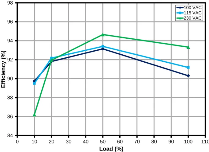
システム効率: 92.1%、 93.4%、91.1% (負荷が 20、50、100%、115 VAC 時)
システム効率: 91.9%、 94.6%、93.3 % (負荷が 20、50、100%、230 VAC 時)
特許情報 ここで提示した製品及びアプリケーション (製品の外付け周辺回路及びトランス構造も含む) は、米国及び他国の特許の対象である場 合 が あ り ま す 。 ま た 、 Power Integrations に 譲 渡 され た 米 国 及び 他 国 の 出 願 中 特許 の 対 象 であ る 場 合 が あ り ま す 。 Power Integrations の 持 つ 特 許 の 全 リ ス ト は 、 www.powerint.com に 掲 載 さ れ ま す 。 Power Integrations は 、 <http://www.powerint.com/ip.htm> に定めるところに従って、特定の特許権に基づくライセンスを顧客に許諾します。目次
1
はじめに ... 5
2
電源仕様 ... 7
3
回路図 ... 8
4
回路の説明... 11
4.1
入力フィルタ、昇圧型コンバータ、バイアス回路 ... 11
4.1.1
EMI フィルタ ... 11
4.1.2
突入電流制限 ... 11
4.1.3
メイン PFC コンバータ ... 11
4.1.4
待機電源 ... 12
4.2
LLC コンバータ ... 13
4.3
一次側... 13
4.4
同期整流 ... 15
5
PCB レイアウト ... 17
6
部品表 ... 19
7
ヒートシンク仕様 ... 23
7.1
LLC ヒート シンク ... 23
7.1.1
LLC ヒート シンク アセンブリ図面 ... 23
7.1.2
PFS ヒート シンク アセンブリ図面 ... 24
7.1.3
ブリッジ整流器ヒート シンク アセンブリ図面 ... 25
8
磁気部品 ... 26
8.1
PFC チョーク (L3) の仕様 ... 26
8.1.1
回路図 ... 26
8.1.2
電気仕様 ... 26
8.1.3
材料 ... 26
8.1.4
PFC インダクタの最終組み立て ... 26
8.2
LLC トランス (T1) の仕様 ... 27
8.2.1
回路図 ... 27
8.2.2
電気仕様 ... 27
8.2.3
材料 ... 27
8.2.4
構造図 ... 28
8.2.5
巻線方法 ... 28
8.3
待機電源トランス (T2) の仕様 ... 29
8.3.1
回路図 ... 29
8.3.2
電気仕様 ... 29
8.3.3
材料 ... 29
8.3.4
トランスの構造図 ... 30
8.3.5
トランスの製造方法 ... 30
8.4
出力インダクタ (L4) の仕様 ... 31
8.4.1
回路図 ... 31
8.4.2
電気仕様 ... 31
8.4.3
材料 ... 31
9
LLC コンバータ設計計算シート ... 32
10
待機電源コンバータ設計計算シート ... 39
11
力率コントローラ 設計計算シート ... 42
12
性能データ ... 47
12.1
システム効率 ... 47
12.2
力率 ... 48
12.3
THD ... 49
12.4
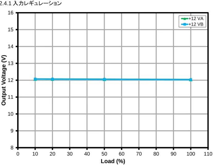
出力レギュレーション ... 50
12.4.1
入力レギュレーション ... 50
12.4.2
負荷レギュレーション ... 51
13
入力電流高調波対 EN 61000-3-2 クラス D 規格 ... 52
14
波形 ... 54
14.1
入力電圧と入力電流 ... 54
14.2
LLC 一次側電圧と電流 ... 54
14.3
PFC 通常動作時のスイッチング電圧と電流 ... 55
14.4
起動時の AC 入力電流と PFC 出力電流 ... 56
14.5
LLC 回路の起動 (CR モード) ... 56
14.6
LLC 回路の停止 ... 57
14.7
LLC 出力短絡保護回路 ... 58
14.8
メイン及び待機電源起動 (CR モード) ... 58
14.9
同期電流回路 FET ドレインとゲート電圧 ... 59
14.10
出力リップルの測定 ... 60
14.10.1
リップルの測定方法 ... 60
14.10.2
最大負荷時の出力リップル波形 ... 61
14.10.3
無負荷時のリップル波形 ... 61
14.11
メイン出力負荷ステップ応答 ... 62
14.12
待機出力負荷ステップ応答 ... 63
15
伝導 EMI ... 64
15.1
EMI のセットアップ ... 64
15.1.1
EMI 試験のための電源準備 ... 64
15.1.2
EMI 試験のセットアップ ... 65
15.2
EMI スキャン ... 66
16
ゲイン位相測定 ... 68
17
付録 ... 69
17.1
リレー ケーブルの準備 ... 69
17.2
PFC インダクタの組み立て ... 70
18
改訂履歴 ... 71
重要なお知らせ:
この電源は絶縁に関する安全要件を満たすよう設計されていますが、評価プロトタイプは認証
機関の承認を得られていません。従って、すべての試験は、プロトタイプ電源に絶縁トランスを
使用して、AC 入力を供給する必要があります。
1
はじめに
この技術レポートには、12 V、19.71 A メイン コンバータ及び 12 V、1.5 A 待機電源コンバータ、
及び 90 VAC ~ 265 VAC PC 電源の設計例が記載されています。同電源は、PFS 力率回路
と Power Integration の HiperPFS-2 及び HiperLCS ファミリーのデバイスを使用する LCS 出
力部を組み合わせた汎用評価ボードとしても使用できます。
この設計では、PFC フロントエンド用 PFS7328H IC 及び絶縁型フライバック待機電源で使用
される TNY279PG を使用しています。LCS703HG IC は、LLC コンバータに使用されます。
Figure 1 – DER-385 Photograph, Top View.
Figure 3 – DER-385 Input Connector.
注:C1、C2、C3 は、入力コネクタに配置されました。
このレポートに記載されている回路は、100%、50%、20% 負荷時の力率が 0.9 以上、入力電
圧範囲が 90 VAC ~ 230 VAC に合わせて最適化されています。
2 電源仕様
次のテーブルは、設計の仕様概要です。実際の性能は、「性能データ」のセクションを参照してく
ださい。
概要
記号
最小
標準
最大
単位
コメント
入力
電圧
V
IN90
265
VAC
3 ワイヤ入力。周波数
f
LINE47
50/60
63
Hz
THD
<15
%
最大負荷、115 VAC<15
%
最大負荷、230 VAC力率
PF
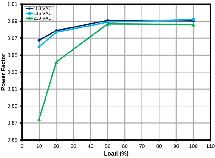
0.97
最大負荷、230 VACメイン コンバータの出力
出力電圧
V
M11.4
12
12.6
V
12VDC ±5%出力リップル
V
RIPPLE(M)120
mV P-P
20 MHz バンド幅出力電流
I
M0.00
19.71
N/A
A
電源は、無負荷動作時に保護されま す待機電源コンバータ の出力
出力電圧
V
SB11.4
12
12.6
V
12 VDC ±5%出力リップル
V
RIPPLE(SB)120
mV P-P
20 MHz バンド幅出力電流
I
SB0.00
1.5
N/A
A
電源は、無負荷動作時に保護されま す出力電力の合計
連続出力電力
P
OUT255
W
効率
システム全体 (最大負荷時)
システム91
93
%
115 VAC、最大負荷時の測定 230 VAC、最大負荷時の測定環境
伝導 EMI
CISPR22/EN55022 クラス B に適合高調波電流
EN 61000-3-2 クラス D周囲温度
T
AMB0
50
oC
熱に関するセクションを参照してください注:この電源は、負荷が 50% 以上の場合に強制空冷を必要とします。
3 回路図
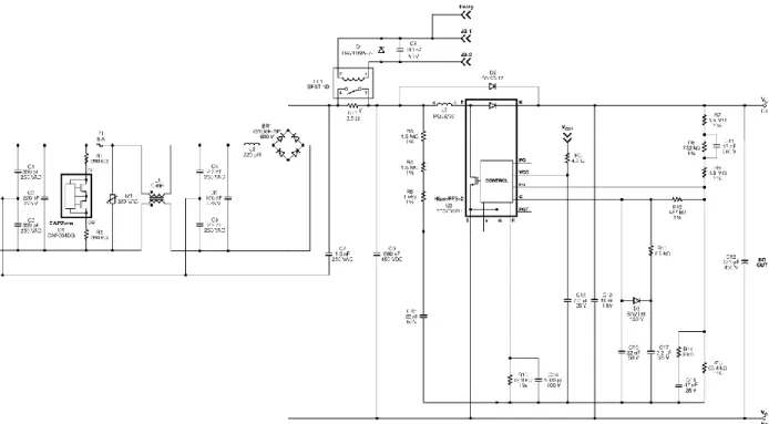
Figure 4 – Schematic DER-385 PC Platinum Power Supply Application Circuit - Input Filter, Bridge
Rectifier Section and PFS Section.
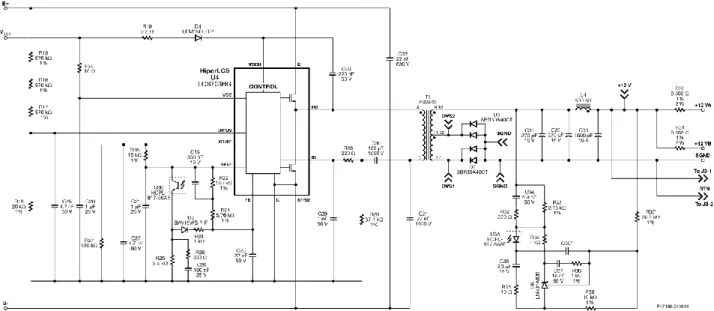
Figure 5 – Schematic DER-385 PC Platinum Power Supply Application Circuit – Main Converter Section.
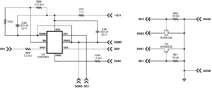
Figure 7 – Schematic DER-385 PC Platinum Power Supply Application Circuit – Sync. Rectifier Section.
Note: * marked components are optional.
4 回路の説明
図 4、5、6 に示す回路では、PC 電源を供給するための 12 V、255 W 力率改善型 LLC 電源
で、Power Integrations の PFS7328H、LCS703HG、TNY279PG、及び CAP004DG (オプシ
ョがン) デバイスを使用します。
4.1
入力フィルタ、昇圧型コンバータ、バイアス回路
図 4 と 5 の回路図は、入力 EMI フィルタ及び PFC コンバータを示します。力率改善回路は、
パワー MOSFET とダイオードを内蔵した PFS7328H PFC コントローラを使用します。図 6 の
回路図は、バイアス回路を示しています。待機電源は TNY279PG を使用した絶縁型フライバ
ック設計です。CAP004DG は、AC 入力電圧がかからない場合にのみ、X コンデンサ C3 及び
C6 を放電し、抵抗 R6 及び R2 の損失を無くします。
4.1.1 EMI フィルタ
ヒューズ F1 は回路保護機能として作動し、故障時に AC 電源から回路をオープンにします。ダ
イオード ブリッジ BR1 は、AC 入力を整流します。コンデンサ C1、C2、C3、C4、C5、C6 及び
C7 とインダクタ L1、L2 は、EMI フィルタを構成し、コモン モードとディファレンシャル モード伝
導ノイズを軽減します。フィルム コンデンサ C9 は、入力デカップリン グコンデンサで、スイッチ
ング周波数及び高調波の入力リップル電流が削減されます。
抵抗 R1、R2、CAPZero IC U1 は、回路から入力電圧が開放され、動作中の消費電力がゼロ
になっているときに、EMI フィルタ コンデンサを放電するための回路です。
金属酸化物バリスタ (MOV) RV1 は、電源に対する入力電圧を効率的に低減することにより、
入力サージ発生時に回路を保護します。
U2 と U4 の一次側ヒート シンクは一次側リターン回路に接続され、伝導及び容量結合されたノ
イズ源及び EMI の発生源にヒート シンクがなることを防ぎます。
4.1.2 突入電流制限
サーミスタ RT1 は、突入電流制限を行います。同サーミスタは、通常動作中にはリレー RL1 に
より短絡され、メイン出力電源の動作開始によりゲートをオンし、効率は約 1 ~ 1.5% 向上しま
す。
メイン出力電源がレギュレーション範囲に達し、RT1 を短絡した場合に、リレー RL1 の電源が
オンになります。
4.1.3 メイン PFC コンバータ
昇圧型コンバータは、昇圧インダクタ L3 と PFS7328H IC U2 で構成されます。このコンバータ
は PFC 昇圧型コンバータとして動作し、入力電流を正弦波に維持し、出力 DC 電圧を制御しま
す。
起動時に、ダイオード D2 は出力コンデンサC12 に突入電流の経路を提供し、スイッチング イ
ンダクタと出力コンデンサ間の共振相互作用を防ぐために、スイッチング インダクタ L3 と PFS
デバイス U2 をバイパスします。
コンデンサ C10 は、EMI改善のために短い、高周波リターン経路を提供し、電源オフ後の U2
MOSFET のドレイン電圧オーバーシュートを削減します。コンデンサ C15 は、U2 VCC ピンを
デカップリング及びバイパスします。
電源の入力電圧は、抵抗 R3、R4、及び R5 を使用して IC U2 で検出されます。コンデンサ
C13 は、IC U2 上の V ピンをバイパスします。
抵抗 R7、R8、R9、及び R13 から構成される出力電圧分圧ネットワークは、コントローラ IC U2
へのフィードバックとして出力電圧に比例した電圧を提供します。コンデンサ C11 は、PFC 回
路のアンダーシュートまたはオーバーシュート時に U2 FB ピンに高速 dv/dt フィードバックを行
います。
抵抗 R12 とコンデンサ C17 は、制御ループのメインポールとなります。C18、C16 及び R14
は高周波ノイズを軽減します。
コンデンサ C17 と直列した抵抗 R11 は、低周波補償ゼロ点を提供し、ダイオード D3 は誤って
ショートした C17 による誤動作を防止します。
4.1.4 待機電源
部品 U7、T2、D11、C45、D8 及び VR1 は、シンプルな絶縁型フライバック電源で構成され、待
機電源となります。トランス T2 は、EF20 コアを使って設計されました。
ON/OFF 制 御 機 能 を 使 用 す る こ と に よ り 、 U7 は ス イ ッ チ ン グ サ イ ク ル を ス キ ッ プ し 、
ENABLE/UNDERVOLTAGE (EN/UV) ピンへのフィードバックに基づいた出力電圧を制御しま
す。EN/UV ピン電流は、それぞれのスイッチング サイクル直前にサンプリングされ、そのスイッ
チング サイクルが有効または無効になっているかどうかを確認します。EN/UV ピン電流が 115
A 以下の場合は、次のスイッチング サイクルが開始し、MOSFET を通る電流が内部カレント
リミットのスレッシュホールドに達した場合に、終了します。均等にスイッチング サイクルを拡散
し、まとまったパルスの発生を防止するために、EN/UV ピン スレッシュホールド電流は、前のサ
イクル時の状態に応じて、115
A ~ 60
A に変調されます。コントローラ内のステートマシン
は、電源から要求される負荷に応じて、パワー MOSFET のカレント リミットのスレッシュホール
ドを 4 つのレベルのうちの 1 つに調整します。電源の負荷が減尐すると、カレント リミットのスレ
ッシュホールドも軽減されます。これにより、有効なスイッチング周波数は、トランスの磁束密度
が低減されるまで可聴領域以上に維持されます。標準のトランス製造技術である浸漬ワニス処
理を行うことで、音鳴りが実質上ゼロになります。
ダイオード D11 は、T2 の出力を整流します。出力電圧リップルは、C45 の低 ESR コンデンサ
を使用して最小限に抑えました。後段フィルタ L5 と C46 は、高周波スイッチング ノイズを軽減
します。
メイン出力及び待機電源出力は、システム全体の効率を改善するため、D12 と D13 を使って
低減されました。
電源の出力電圧のレギュレーション設定ポイントは、抵抗 R53、R54、及び U8 基準電圧により
設定されます。抵抗 R50 は、負荷の過渡時の最大電流を制限します。出力電流が設定ポイン
トを上回ると、U6 の LED が順方向にバイアスされます。一次側で、U6 のフォトカプラがオンに
なり、U7 の EN/UV ピンから電流が引き込まれます。各スイッチングサイクルの開始直前に、コ
ントローラは EN/UV ピン電流を確認します。EN/UV ピンから流れる電流が 115 A を上回ると、
そのスイッチング サイクルは停止されます。スイッチング サイクルが有効または無効が繰り返
されると、出力電圧はレギュレーション設定ポイントに極めて近い値に維持されます。
4.2
LLC コンバータ
図 5 の回路図は、LCS703HG を使って実装される 12 V、237 W LLC DC-DC コンバータを示
しています。
4.3
一次側
集積回路 U4 には、LLC 共振ハーフブリッジ (HB) コンバータに必要な制御回路、ドライバ、出
力 MOSFET が集積されています。U4 の HB 出力は、ブロッキング及び共振コンデンサ (C24)
経由で出力トランス T1 を駆動します。このコンデンサは、動作リップル電流に対応しており、異
常状態時の高電圧に対応します。
トランス T1 は 115
H の漏れインダクタンスに対応し、設計されました。この値と共振コンデン
サ C24 の値から、以下の方程式に基づき一次直列共振周波数が 90 kHz 以下に設定されま
す。
R L RC
L
f
28
.
6
1
この方程式の R は、直列共振周波数 (単位ヘルツ) です。LL は、トランスの漏れインダクタンス
(単位ヘンリー) です。そして、CR は、共振コンデンサ (C24) の値 (単位ファラッド) です。
トランスの巻線比は、最大負荷時の定格入力電圧の動作周波数が前述の共振周波数をわず
かに下回るように一次巻線を調整することによって設定されました。
90 kHz の動作周波数は、トランスのサイズ、セラミック コンデンサを可能にする出力フィルタ コ
ンデンサ、及び効率の優れた妥協点となっています。
また、二次巻線数は、コア損失と銅損失の間のバランスを考慮して選択されました。一次巻線
には AWG #38 リッツ線が使用され、二次巻線には AWG #40 リッツ線が使用されました。この
組み合わせにより動作周波数 (90 kHz 以下) で高効率が実現されます。それぞれのリッツ巻線
ゲージ内のストランド数は、巻線の収まり具合と銅損失間のバランスを考え、選択されました。
選択されたコア材料は PC95 (TDK 製) です。この材料は性能を向上させ、低損失を実現しま
す。
部品 D4、R19、及び C23 はブートストラップ回路を構成して、U4 の内蔵ハイサイド ドライバを
供給します。
部品 C20 及び R20 は、U4 の VCC 電源である +12 V 入力のフィルタ及びバイパスを実現しま
す。注:15 V 以上の V
CC電圧は U1 を損傷する場合があります。
分圧器 R15、R16、R17、R18 は、U4 の高電圧ターンオン、ターンオフ、及び過電圧スレッシュ
ホールドを設定します。分圧器の値は、入力過電圧ターン オフ ポイント 473 VDC で、LLC ター
ンオン ポイントが 360 VDC、ターンオフ ポイントが 285 VDC となるように選択されています。
コンデンサ C22 は +380 V 入力用の高周波バイパス コンデンサで、U4 の D 及び S1/S2 ピン
間で短い配線で接続されます。
コンデンサ C30 は、C24 とともに電流分割器を形成します。C31 は、一次電流の一部をサンプ
リングするのに使用されます。抵抗 R29 がこの電流を検出します。その結果信号は、R28 と
C29 によってフィルタされます。コンデンサ C30 の定格は、異常状態時のピーク電圧に対応す
る必要があります。また、C12 には、金属化フィルム、SL セラミック、NPO セラミック、COG セ
ラミックなどの安定した低損失誘電体を使用する必要があります。DER-385 で使用されている
コンデンサは、CCFL チューブのドライバで一般的に使用される、"SL" 温度特性のセラミック デ
ィスクです。選択された値に基づいて、以下の方程式から 1 サイクル (高速) のカレントリミット
が 6.52 A に、7 サイクル (低速) のカレントリミットが 3.62 A に設定されます。
29
30
24
30
5
.
0
R
C
C
C
I
CL
ICL は、7 サイクルのカレントリミット (単位アンペア) です。R29 は、カレントリミット抵抗 (単位オ
ーム) です。C24 と C30 は、それぞれ共振コンデンサと電流サンプリング コンデンサの値 (単
位ナノファラッド) です。1 サイクルのカレントリミットについては、上記の方程式で 0.5 V の代わ
りに 0.9 V を使用します。
抵抗 R28 は、推奨最小値の 220 に設定されています。C29 の値は、ノイズによる誤動作を
防ぐために 1 nF に設定されています。ただし、この値は、前述の計算によるカレントリミット設
定値に大きく影響するほど高くはありません。これらの部品は、最大の効果が得られるように IS
ピンの近くに配置する必要があります。IS ピンは負電流を許容できるので、電流センスに複雑
な整流スキームは必要ありません。
R23 と R27 のテブナン等価回路は、デッドタイムを 625 nS に設定し、U4 の最大動作周波数
を 434 kHz に設定します。U4 の FMAX 入力は、C27 によってフィルタされます。また、R23 と
R27 の組み合わせにより、U4 に対してバースト モード "2" が選択されます。この結果、下側と
上側のバースト スレッシュホールド周波数がそれぞれ 160 kHz と 187 kHz に設定されます。
FEEDBACK ピンには、FEEDBACK ピンに流れる 1 A あたり 2.6 kHz という近似特性があり
ます。FEEDBACK ピンへの電流は、U4 の動作周波数を増加させるため、出力電圧を軽減し
ます。R21 と R22 の直列接続により、U9 の最小動作周波数が 62 kHz 以下に設定されます。
この値は、最大負荷かつ最小整流コンデンサ電圧でのレギュレーションに必要な周波数より低
く設定されています。抵抗 R21 は C19 によってバイパスされます。これは、フィードバック ルー
プがオープンの時に、最初により大きな電流が FEEDBACK ピンに流れるようにすることによっ
て、起動時の出力ソフトスタートを実現するためです。この結果、スイッチング周波数が高い周
波数から始まり、その後、出力電圧がレギュレーションになるまで小さくなります。抵抗 R21 は
通常、ソフトスタート時の初期周波数が R23 で設定される最大スイッチング周波数と等しくなる
ように、R23 と同じ値に設定されます。R22 の値がこれより小さいと、入力電圧が印加されたと
き、スイッチング開始前にディレーが発生します。
フォトカプラ U3 は、FEEDBACK ピンへの最大フォトカプラ電流を制限する R24 経由で U4
FEEDBACK ピンを駆動します。コンデンサ C28 は、FEEDBACK ピンをフィルタします。抵抗
R25 は、フォトカプラ出力に負荷をかけて比較的高い電源消費電流で動作させ、ゲインを増や
します。抵抗 R24 及び R25 は、大信号ステップ応答とバースト モード出力リップルも改善しま
す。ダイオード D5 は、FMAX/ソフトスタート回路から R25 を分離します。
4.4
同期整流
トランス T1 の出力は、同期整流コントローラ U9、MOSFET Q2、Q3、ダイオード D6、D7 及び
コンデンサ C31、C32 を使用して、整流及びフィルタリングされます。これらのコンデンサは有
機ポリマー コンデンサであり、出力リップル電流定格のために慎重に選ばれています。同期整
流は、80 PLUS Platinum 効率基準を満たすために、選択されています。MOSFETs Q2 と Q3
は、より長い MOSFET 導通期間と高効率を実現するために、選択されています。同期整流器
コントローラと関連する部品のレイアウトを決める際には、細心の注意を払う必要があります。
-12 mV (-25 mV の代わりに) ドレイン検出のターンオフ スレッシュホールドが、指定された負
荷でより長い MOSFET 導通期間を実現するために選択されています。MOSFET のオフ時に
MOSFET のボディ ダイオード導通を避けることによりさらに効率を改善するために、ダイオード
D6 と D7 が 使われています。L4 及び C33 は出力後段フィルタです。
抵抗 R37 及び R38 は、U5 基準電圧とともに、電源の出力電圧を設定します。エラー アンプ
U5 は、R33 経由でフィードバック フォトカプラ U3 を駆動します。部品 C34、C26、C37、R33、
R32、R36 及び R26 は、電源のゲイン位相特性を決定します。これらの値は、定格及び極端な
負荷や入力電圧の組み合わせでも安定動作を実現するように選択されました。フォトカプラ U3
の LED で電流が発生していない場合、抵抗 R34 により、必要な最小動作電流を U3 に流すこ
とができます。部品 C35 と R35 は、ターンオン時の出力のオーバーシュートを解消するソフト
スタート回路を提供するために使用されます。
5 PCB レイアウト
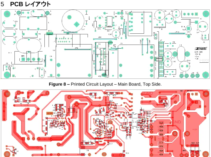
Figure 8 – Printed Circuit Layout – Main Board, Top Side.
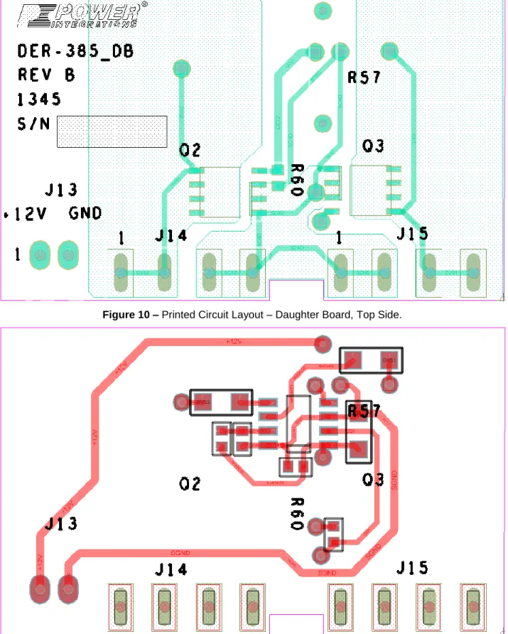
Figure 10 – Printed Circuit Layout – Daughter Board, Top Side.
6 部品表
Item Qty Ref Des Description Mfg Part Number Mfg Main Board BOM
1 1 BR1 800 V, 8 A, Bridge Rectifier, GBU Case GBU8K-BP Micro Commercial 2 2 C1 C2 330 pF, 250 VAC, Film, X1Y1 CD90-B2GA331KYNS TDK 3 1 C3 220 nF, 275VAC, Film, X2 R46KI322050M2K Kemet 4 2 C4 C5 2.2 nF, Ceramic, Y1 440LD22-R Vishay 5 1 C6 150 nF, 275 VAC, Film, X2 LE154-M OKAYA
6 1 C7 1.5 nF, Ceramic, Y1 440LD15-R Vishay
7 2 C8 C41 100 nF 50 V, Ceramic, X7R, 0603 C1608X7R1H104K TDK 8 1 C9 680 nF, 450 VDC, Disc Ceramic ECQ-E2W684KH Panasonic 9 1 C10 10 nF, 1 kV, Ceramic, X7R, 1812 VJ1812Y103KXGAT Vishay 10 1 C11 47 nF, 200 V, Ceramic, X7R, 1206 12062C473KAT2A AVX 11 1 C12 220 F, 450 V, Electrolytic, (22 x 45) ESMQ451VSN221MP45S United Chemi-con 12 3 C13 C16 C28 22 nF 50 V, Ceramic, X7R, 0603 C1608X7R1H223K TDK 13 1 C14 1000 pF, 100 V, Ceramic, COG, 0603 C1608C0G2A102J TDK 14 2 C15 C35 3.3 F, 25 V, Ceramic, X7R, 0805 C2012X7R1E335K TDK 15 1 C17 2.2 F, 25 V, Ceramic, X7R, 0805 C2012X7R1E225M TDK 16 2 C18 C48 47 nF 25 V, Ceramic, X7R, 0603 CC0603KRX7R8BB473 Yago 17 1 C19 330 nF, 16 V, Ceramic, X7R, 0603 C1608X7R1C334K080AC TDK 18 2 C20 C21 1 F, 25 V, Ceramic, X5R, 0805 C2012X5R1E105K TDK 19 1 C22 22 nF, 630 V, Ceramic, X7R, 1210 GRM32QR72J223KW01L Murata 20 1 C23 220 nF 50 V, Ceramic, X7R, 0603 CGA3E3X7R1H224K TDK 21 1 C24 27 nF, 1600 V, Film BFC238350273 Vishay 22 2 C25 C27 4.7 nF 50 V, Ceramic, X7R, 0603 GRM188R71H472KA01D Murata 23 1 C26 100 nF, 25 V, Ceramic, X7R, 0805 08053C104KAT2A AVX 24 1 C29 1 nF, 50 V, Ceramic, X7R, 0805 08055C102KAT2A AVX 25 1 C30 100 pF, 1000 V, Ceramic, NPO, 1206 102R18N101JV4E Johanson Dielectrics
26 2 C31 C32 270 F, 16 V, Al Organic Polymer, Gen.
Purpose, 20% RL81C271MDN1KX Nichicon 27 1 C33 1500 F, 16 V, Electrolytic, Low ESR, 37 m,
(10 x 30) ELXZ160ELL152MJ30S Nippon Chemi-Con 28 1 C34 6.8 nF, 50 V, Ceramic, X7R, 0805 CC0805KRX7R9BB682 Yageo 29 1 C37 10 nF 50 V, Ceramic, X7R, 0603 C0603C103K5RACTU Kemet 30 1 C39 330 F, 25 V, Electrolytic, Low ESR, 90 m, (8 x
15) ELXZ250ELL331MH15D Nippon Chemi-Con 31 1 C40 100 nF, 50 V, Ceramic, X7R, 0805 CC0805KRX7R9BB104 Yageo 32 1 C42 220 pF, 50 V, Ceramic, X7R, 0805 CC0805KRX7R9BB221 Yageo 33 1 C43 33 nF, 400 V, Film ECQ-E4333KF Panasonic 34 1 C44 470 pF, 250 V, Ceramic,GCM, 0805 GCM21A7U2E471JX01D Murata 35 1 C45 1000 F, 16 V, Electrolytic, (10 x 16) KMG16WV1000UF10X16 Sam Young 36 1 C46 330 F, 16 V, Electrolytic, Low ESR, 120 m, (8
x 12) ELXZ160ELL331MH12D Nippon Chemi-Con 37 2 D1 D3 130 V, 5%, 250 mW, SOD-123 BAV116W-7-F Diodes, Inc. 38 1 D2 DIODE GEN PURPOSE, 800 V, 8 A ,SMC S8KC-13 Diodes, Inc 39 1 D4 600 V, 1 A, Ultrafast Recovery, 75 ns, SOD-123 UFM15PL-TP Micro Commercial 40 1 D5 75 V, 0.15 A, Switching, SOD-323 BAV16WS-7-F Diodes, Inc. 41 2 D6 D7 Diode SBR 40 V, 30 A, TO220AB SBR30A40CT Diodes, Inc. 42 1 D8 1000 V,1 A, Fast Recovery Diode, GP DO-41 FR107G-B Rectron 43 1 D9 200 V, 1 A, Fast Recovery, 150 ns, SMA RS1D-13-F Diodes, Inc. 44 1 D10 600 V, 1 A, Standard Recovery, SMA S1J-13-F Diodes, Inc.
45 1 D11 Diode SBR 100 V, 5 A, ITO, 220AB SBR10U100CTFP Diodes, Inc. 46 2 D12 D13 20 V, 5 A, Schottky, DO-201AD SB520-E3/54 Vishay 47 1 F1 5 A, 250 V, Slow, Long Time Lag, RST RST 5 Belfuse 48 3
GREASE1-GREASE3 Thermal Grease, Silicone, 5 oz Tube CT40-5 ITW Chemtronics 49 1 HEATSHRIN
K1 Heat Shrink 3/16 IN X 4 FT BLACK FIT221B-3/16 BK100 Alpha Wire 50 1 HS1 Heat Sink, Custom, Al, 3003, 0.090" Thk Custom 51 1 HS2 Heat Sink, Custom, Al, 3003, 0.090" Thk Custom 52 1 HS3 Heat Sink, Custom, Al, 3003, 0.078" Thk Custom 53 6 J1 J2 J9-J12 PCB Terminal Hole, #18 AWG N/A N/A 54 2 J3 J4 2 Position (1 x 2) header, 0.1 pitch, Vertical 22-23-2021 Molex 55 1 J5 4 Position (1 x 4) header, 0.156 pitch, Vertical 26-48-1045 Molex 56 1 J8 2 Position (1 x 2) header, 0.1 pitch, Vertical Molex 57 3 JP1 JP7 JP9 Wire Jumper, Insulated, #24 AWG, 0.4 in C2003A-12-02 Gen Cable 58 3 JP2 JP10
JP12 Wire Jumper, Insulated, #24 AWG, 0.5 in C2003A-12-02 Gen Cable 59 1 JP3 Wire Jumper, Insulated, #24 AWG, 1.0 in C2003A-12-02 Gen Cable 60 1 JP4 Wire Jumper, Insulated, #24 AWG, 1.2 in C2003A-12-02 Gen Cable 61 2 JP5 JP8 Wire Jumper, Insulated, #24 AWG, 0.3 in C2003A-12-02 Gen Cable 62 1 JP6 Wire Jumper, Insulated, #24 AWG, 0.9 in C2003A-12-02 Gen Cable 63 2 JP11 JP13 Wire Jumper, Insulated, #24 AWG, 0.6 in C2003A-12-02 Gen Cable 64 3 JP14-JP16 Wire Jumper, Insulated, TFE, #22 AWG, 0.3 in C2004-12-02 Alpha 65 1 L1 9 mH, 5 A, Common Mode Choke T22148-902S P.I. Custom Fontaine Technologies 66 1 L2 220 H, 3.6 A, Vertical Toroidal 2216-V-RC Bourns 67 1 L3 Bobbin, PQ32/20, Vertical, 12 pins YC-PQ3220 Ying Chin 68 1 L4 Custom, DER-385 Main Post Filter Inductor, 500
nH
69 1 L5 2.2 H, 6.0 A RFB0807-2R2L Coilcraft 70 4
MTG_HOLE1-MTG_HOLE4 Mounting Hole No 4
71 4 P3-P6 CONN TERM FEMALE #22-30 AWG TIN 08-50-0113 Molex 72 1 Q1 NPN, Small Signal BJT, GP SS, 40 V, 0.6 A,
SOT-23 MMBT4401LT1G Diodes, Inc.
73 2 R1 R2 390 k, 5%, 1/4 W, Thick Film, 1206 ERJ-8GEYJ394V Panasonic 74 3 R3 R4 R7 1.50 M, 1%, 1/4 W, Thick Film, 1206 ERJ-8ENF1504V Panasonic 75 3 R5 R45 R46 1.00 M, 1%, 1/4 W, Thick Film, 1206 ERJ-8ENF1004V Panasonic 76 1 R6 4.7 , 5%, 1/8 W, Thick Film, 0805 ERJ-6GEYJ4R7V Panasonic 77 1 R8 732 k, 1%, 1/4 W, Thick Film, 1206 ERJ-8ENF7323V Panasonic 78 1 R9 1.60 M, 1%, 1/4 W, Thick Film, 1206 ERJ-8ENF1604V Panasonic 79 1 R10 49.9 k, 1%, 1/16 W, Thick Film, 0603 ERJ-3EKF4992V Panasonic 80 1 R11 7.5 k, 5%, 1/10 W, Thick Film, 0603 ERJ-3GEYJ752V Panasonic 81 1 R12 487 k, 1%, 1/16 W, Thick Film, 0603 ERJ-3EKF4873V Panasonic 82 1 R13 60.4 k, 1%, 1/16 W, Thick Film, 0603 ERJ-3EKF6042V Panasonic 83 1 R14 3 k, 5%, 1/10 W, Thick Film, 0603 ERJ-3GEYJ302V Panasonic 84 2 R15 R16 976 k, 1%, 1/4 W, Thick Film, 1206 ERJ-8ENF9763V Panasonic 85 1 R17 976 k, 1%, 1/4 W, Metal Film MFR-25FBF-976K Yageo 86 1 R18 20 k, 1%, 1/16 W, Thick Film, 0603 ERJ-3EKF2002V Panasonic 87 1 R19 2.2 , 5%, 1/8 W, Thick Film, 0805 ERJ-6GEYJ2R2V Panasonic 88 1 R20 10 , 5%, 1/10 W, Thick Film, 0603 ERJ-3GEYJ100V Panasonic 89 1 R21 5.76 k, 1%, 1/16 W, Thick Film, 0603 ERJ-3EKF5761V Panasonic 90 1 R22 140 k, 1%, 1/16 W, Thick Film, 0603 ERJ-3EKF1403V Panasonic 91 1 R23 15 k, 1%, 1/4 W, Metal Film MFR-25FBF-15K0 Yageo
92 4 R24 R34 R36 R51 1 k, 5%, 1/10 W, Thick Film, 0603 ERJ-3GEYJ102V Panasonic 93 1 R25 2.4 k, 5%, 1/4 W, Thick Film, 1206 ERJ-8GEYJ242V Panasonic 94 1 R26 330 , 5%, 1/8 W, Thick Film, 0805 ERJ-6GEYJ331V Panasonic 95 1 R27 130 k, 5%, 1/10 W, Thick Film, 0603 ERJ-3GEYJ134V Panasonic 96 1 R28 220 , 5%, 1/8 W, Thick Film, 0805 ERJ-6GEYJ221V Panasonic 97 1 R29 37.4 , 1%, 1/8 W, Thick Film, 0805 ERJ-6ENF37R4V Panasonic 98 2 R30 R31 0.002 , 1%, 2 W, Thick Film, 2512 PMR100HZPFV2L00 Rohm Semi 99 1 R32 220 , 5%, 1/10 W, Thick Film, 0603 ERJ-3GEYJ221V Panasonic 100 1 R33 2.15 k, 1%, 1/16 W, Thick Film, 0603 ERJ-3EKF2151V Panasonic 101 1 R35 10 , 5%, 1/8 W, Thick Film, 0805 ERJ-6GEYJ100V Panasonic 102 1 R37 38.3 k, 1%, 1/4 W, Thick Film, 1206 ERJ-8ENF3832V Panasonic 103 2 R38 R54 10 k, 1%, 1/16 W, Thick Film, 0603 ERJ-3EKF1002V Panasonic 104 1 R39 1 , 5%, 1/4 W, Carbon Film CFR-25JB-1R0 Yageo 105 1 R41 3.01 k, 1%, 1/4 W, Thick Film, 1206 ERJ-8ENF3011V Panasonic 106 1 R42 23.7 k, 1%, 1/4 W, Metal Film MFR-25FBF-23K7 Yageo 107 1 R43 1.2 M, 5%, 1/8 W, Thick Film, 0805 ERJ-6GEYJ125V Panasonic 108 2 R44 R47 1 M, 1%, 1/4 W, Metal Film MFR-25FBF-1M00 Yageo 109 1 R48 100 , 5%, 1/10 W, Thick Film, 0603 ERJ-3GEYJ101V Panasonic 110 1 R49 10 , 1%, 1/4 W, Thick Film, 1206 ERJ-8ENF10R0V Panasonic 111 1 R50 200 , 1%, 1/4 W, Thick Film, 1206 ERJ-8ENF2000V Panasonic 112 1 R52 16.9 k, 1%, 1/16 W, Thick Film, 0603 ERJ-3EKF1692V Panasonic 113 1 R53 36.5 k, 1%, 1/16 W, Thick Film, 0603 ERJ-3EKF3652V Panasonic 114 1 RL1 RELAY GEN PURPOSE SPST 8 A 12 V G6RL-1A-ASI-DC12 OMRON 115 1 RT1 NTC Thermistor, 2.5 , 5 A SL10 2R505 Ametherm 116 1 RTV1 RTV 670810.10ZCLR Silico RTV670810.10ZCLR GE 117 1 RV1 320 V, 23 J, 10 mm, RADIAL V320LA10P Littlefuse
118 2 SCREW1 SCREW2 SCREW MACHINE PHIL 4-40 X 5/16 SS PMSSS 440 0031 PH Building Fasteners
119 5 SCREW3-SCREW7 SCREW MACHINE PHIL 4-40 X 1/4 SS PMSSS 440 0025 PH Building Fasteners
120 4
STDOFF1-STDOFF4 Standoff Hex, 4-40, 0.375" L, Al, F/F 1892 Keystone 121 1 T1 Bobbin, PQ32/30, Vertical, 12 pins BQ32/30-1112CPFR TDK 122 1 T2 Bobbin, EF20, Vertical, 10 pins
123 1 U1 CAPZero, SO-8C CAP004DG Power Integrations 124 1 U2 HiperPFS-2, ESIP16/13 PFS7328H Power Integrations 125 2 U3 U6 Optocoupler, TRAN OUT 4-SMD HCPL-817-56AE Avago Technologies 126 1 U4 HiperLCS, ESIP16/13 LCS703HG Power Integrations 127 2 U5 U8 IC, REG ZENER SHUNT ADJ SOT-23 LM431AIM3/NOPB National Semi 128 1 U7 TinySwitch-III, DIP-8C TNY279PG Power Integrations 129 1 VR1 150 V, 5 W, 5%, TVS, DO204AC (DO-15) P6KE150A Littlefuse 130 1 VR2 9.1 V, 5%, 150 mW, SSMINI-2 DZ2S091M0L Panasonic 131 1 VR3 13 V, 5%, 225 mW, SOT23 BZX84C13LT1G On Semi 132 3
WASHER1-WASHER3 WASHER FLAT #4 SS FWSS 004 Building Fasteners
133 3 WIRE14AWG _INS_J1 WIRE14AWG _INS_J11 WIRE14AWG _INS_J12
Wire, UL1015, #14 AWG, Blk, PVC, Length To
be specified by designer 1015-14/41-00 Anixter
134 3
WIRE14AWG _INS_J2 WIRE14AWG
Wire, UL1015, #14 AWG, Red, PVC, Length To
_INS_J9 WIRE14AWG
_INS_J10 135 1 WIRE22AWG
_INS1
Wire, UL1007, #22 AWG, Blk, PVC, Length To
be specified by designer 1007-22/7-00 Anixter 136 1 WIRE22AWG
_INS2
Wire, UL1007, #22 AWG, Red, PVC, Length To
be specified by designer 1007-22/7-02 Anixter
Daughter Board BOM
1 1 C49 100 nF, 25 V, Ceramic, X7R, 0603 VJ0603Y104KNXAO Vishay 2 1 C50 100 nF, 25 V, Ceramic, X7R, 1206 C1206F104K3RACTU Kemet 3 1 J13 2 Position (1 x 2) header, 0.1 pitch, RT angle,
gold TSW-102-08-L-S-RA Samtec Inc
4 2 J14 J115 4.00 mm Header, 4 Circuits, 3.81 mm Tail Length 75730-0204 Molex 5 2 Q2 Q3 40 V, 85 A N-Channel, DFN5X6 AON6232 Alpha & Omega Semi 6 1 R56 270 k, 5%, 1/10 W, Thick Film, 0603 ERJ-3GEYJ274V Panasonic 7 1 R57 1 , 5%, 1/4 W, Carbon Film CFR-25JB-1R0 Yageo 8 2 R58 R59 1.5 k, 5%, 1/4 W, Thick Film, 1206 ERJ-8GEYJ152V Panasonic 9 2 R60 R61 10 k, 5%, 1/10 W, Thick Film, 0603 ERJ-3GEYJ103V Panasonic 10 1 U9 IC SMART DVR SYNC RECT 8-SOIC SRK2000DTR ST Micro
7 ヒートシンク仕様
7.1
LLC ヒート シンク
8 磁気部品
8.1
PFC チョーク (L3) の仕様
8.1.1 回路図
Figure 12 – PFC Choke Electrical Diagram.
8.1.2 電気仕様
Inductance
Pins 1-FL1 measured at 100 kHz, 0.4 V
RMS.500
H ±5%
8.1.3 材料
Item
Description
[1]
Core: PQ32/20, PC44 core material.
[2]
Served litz wire: #40 / #38 AWG.
8.1.4 PFC インダクタの最終組み立て
8.2
LLC トランス (T1) の仕様
8.2.1 回路図
WD3: (Primary) WD1: (1st Secondary) WD2: (2nd Secondary) 7 10 9 12 4 6 2T –300/0.1mm Unserved Litz 2T –300/0.1mm Unserved Litz 34T – 75/#40 Served LitzFigure 14 – LLC Transformer Electrical Diagram.
8.2.2 電気仕様
Electrical Strength
1 second, 60 Hz, from pins 4-6 and pins 7-12.
3000 VAC
Primary Inductance
Pins 4-6, all other windings open, measured at 100 kHz,
0.4 V
RMS.
650
H ±5%.
Resonant Frequency
Pins 4-6, all other windings open
1400 kHz (Min.)
Primary Leakage
Inductance
Pins 4-6, with pins 7,9,10 and 12 shorted, measured at
100
kHz, 0.4 V
RMS.
115
H ±10%.
8.2.3 材料
Item
Description
[1]
Core: PQ32/30-TDK PC95 and gapped ALG 560 nH/T
2.
[2]
Bobbin: PQ32/30-Vertical, 12 pins (6/6).
[3]
Magnet wire: 75 / #40 AWG Served Litz.
[4]
Magnet wire: 300 / 0.1 mm Unserved Litz; or 300/#38 AWG Unserved Litz.
[5]
Margin tape: 3M 44, margin tape, cream, 6.0 mm wide; or equivalent.
[6]
Tape: 3M 1298 Polyester Film, 8.0 mm wide, 2.0 mils thick; or equivalent.
[7]
Tape: 3M 1298 Polyester Film, 18.0 mm wide, 2.0 mils thick or equivalent.
[8]
Teflon tube: #16, Alpha Wire TFT-200016.
8.2.4 構造図
WD1: (1st Secondary)
to be twisted and wound in parallel with...
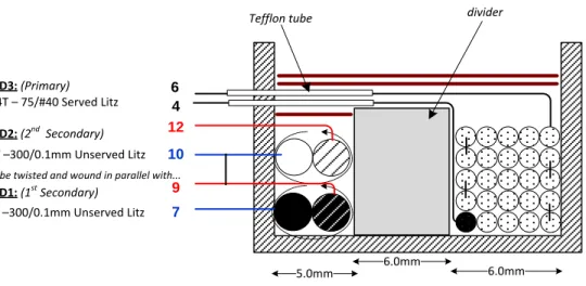
WD3: (Primary) 34T – 75/#40 Served Litz WD2: (2nd Secondary) 2T –300/0.1mm Unserved Litz 7 10 9 12 4 6 6.0mm divider 2T –300/0.1mm Unserved Litz 6.0mm 5.0mm Tefflon tube
Figure 15 – LLC Transformer Build Diagram.
8.2.5 巻線方法
Winding Preparation
Place the bobbin on the mandrel with the pin side is on the left side.
Winding direction is clockwise direction.
Place margin tape item [5] on the bobbin with to create 2 chambers with location
shown as in fig. 2 above.
Prepare 2 strands of wire item [4] ~ 8” length, tin ends. Label one strand to
distinguish from other and designate it as FL1, FL2. Other strand will be
designated as FL3 and FL4. Twist these 2 strands together ~8 twists evenly
along length leaving 1” free at each end. Tin other ends.
WD1 & WD2
Secondary
Use wires assembly prepared above, start with FL1 on pin 7 and FL3 on pin 9,
tightly wind 2 turns in left chamber. Finish with FL2 on pin 10 and FL4 in pin 12.
Secure winding with tape item [6].
Insulation
Place 1 layer of tape item [5].
WD3
Primary
Start at pin 4, wind 34 turns of wire item [3] in the right chamber with tight tension
and finish at pin 6. Insert Teflon tubes ~ 20 mm long item [8] for both ends of this
winding.
Insulation
Place 2 layers of tape item [7].
8.3
待機電源トランス (T2) の仕様
8.3.1 回路図
3
2
1
8
10
4
5
WD1 = 1st Primary 54T - #29AWG WD4 = 2nd Primary 35T - #29AWG WD3 = Secondary 9T – 2 x #25AWG_TIW WD3 = Aux 11T – 2 x #31AWGFigure 16 – Transformer Electrical Diagram.
8.3.2 電気仕様
Electrical Strength
1 second, 60 Hz, from pins 1-5 to pins 6-10.
3000 VAC
Primary Inductance
Pins 1-3, all other windings open, measured at 100 kHz,
0.4 V
RMS.
1157
H ±10%
Resonant Frequency
Pins 1-3, all other windings open.
1.2 MHz (Min.)
Leakage Inductance
Pins 1-3, with secondary pins shorted, measured at 100
kHz, 0.4 V
RMS.
15
H (Max.)
8.3.3 材料
Item
Description
[1]
Core: EF20. part #: PC44EF20-Z.
[2]
Bobbin: EF20, Vertical, 10 pins, (5/5).
[3]
Magnet wire: #29 AWG.
[4]
Magnet wire: #31 AWG.
[5]
Magnet wire: #25 AWG Triple Insulated Wire.
[6]
Tape: 3M 1298 Polyester Film, 2 mils thick, 20 mm wide.
[7]
Varnish.
8.3.4 トランスの構造図
3
2
5
4
8
10
2
1
WD1: WD2: WD3: WD4: 54T - #29AWG 35T - #29AWG 11T – 2 x #31AWG 9T – 2 x #25AWG_TIWFigure 17 – Bias Transformer Build Diagram.
8.3.5 トランスの製造方法
Winding
Preparation
Position the bobbin on the mandrel such that the pin side is on the left side of
bobbin mandrel. Winding direction is clock-wise direction
WD1
1
stPrimary
Start at pin 3, wind 54 turns of wire item [3] from left to right with tight tension in
two layers, and terminate at pin 2
Insulation
2 layers of tape item [6]
WD2
Auxiliary
Start at pin 5, wind 11 bi-filar turns of wire item [4] from left to right also with tight
tension in one layer, at the last turn bring the wire back to the left and terminate at
pin 4
Insulation
2 layers of tape item [6]
WD3
Secondary
Start at pin 8 wind 9 bi-filar turns of wire item [5] from left to right also with tight
tension in one layer, at the last turn bring the wire back to the left and terminate at
pin 10
Insulation
2 layers of tape item [6]
WD4
2
ndPrimary
Start at pin 2, wind 35 turns of wire item [3] from right to left with tight tension in
one layer, at the last turn bring the wire back to the right and terminate at pin 1
Insulation
3 layers of tape item [6]
Finish
Assemble, grind the cores to get 1.157 mH, and secure the cores with tape.
Varnish [7]
8.4
出力インダクタ (L4) の仕様
8.4.1 回路図
2T – 3X17AWG
FL1
FL2
Figure 18 – Inductor Electrical Diagram.
8.4.2 電気仕様
Inductance
Pins FL1-FL2, all other windings open, measured at 100 kHz,
0.4 V
RMS.500 nH, ±15%
8.4.3 材料
Item
Description
[1]
Powdered Iron Toroidal Core: Micrometals T60-52.
[2]
Magnet wire: #17 AWG Solderable Double Coated.
9 LLC コンバータ設計計算シート
HiperLCS_042413;Rev.1.3; Copyright Power Integrations 2013
INPUTS INFO OUTPUTS UNITS
HiperLCS_042413_Rev1-3.xls; HiperLCS Half-Bridge, Continuous mode LLC Resonant Converter Design Spreadsheet
Enter Input Parameters
Vbulk_nom 380 380 V Nominal LLC input voltage
Vbrownout 280 V
Brownout threshold voltage. HiperLCS will shut down if voltage drops below this value. Allowable value is between 65% and 76% of Vbulk_nom. Set to 65% for max holdup time
Vbrownin 353 V Startup threshold on bulk capacitor VOV_shut 465 V OV protection on bulk voltage VOV_restart 448 V Restart voltage after OV protection.
CBULK 220.00 220 uF
Minimum value of bulk cap to meet holdup time requirement; Adjust holdup time and Vbrownout to change bulk cap value
tHOLDUP 29.5 ms Bulk capacitor hold up time
Enter LLC (secondary) outputs The spreadsheet assumes AC stacking of the secondaries
VO1 12.00 12.0 V Main Output Voltage. Spreadsheet assumes that this is the regulated output
IO1 19.71 19.7 A Main output maximum current
VD1 0.10 0.10 V Forward voltage of diode in Main output PO1 237 W Output Power from first LLC output
VO2 0.0 V Second Output Voltage
IO2 0.0 A Second output current
VD2 0.70 V Forward voltage of diode used in second output PO2 0.00 W Output Power from second LLC output P_LLC 237 W Specified LLC output power
LCS Device Selection
Device LCS703 LCS Device
RDS-ON (MAX) 1.12 ohms RDS-ON (max) of selected device Coss 312 pF Equivalent Coss of selected device Cpri 40 pF Stray Capacitance at transformer primary Pcond_loss 2.8 W Conduction loss at nominal line and full load Tmax-hs 90 deg C Maximum heatsink temperature
Theta J-HS 8.7 deg C/W Thermal resistance junction to heatsink (with grease and no insulator)
Expected Junction
temperature 115 deg C Expectd Junction temperature Ta max 50 deg C Expected max ambient temperature
Theta HS-A 14 deg C/W Required thermal resistance heatsink to ambient
LLC Resonant Parameter and Transformer Calculations (generates red curve)
Vres_target 380.00 380 V
Desired Input voltage at which power train operates at resonance. If greater than Vbulk_nom, LLC operates below resonance at VBULK.
Po 238 W LLC output power including diode loss Vo 12.10 V Main Output voltage (includes diode drop) for
calculating Nsec and turns ratio
f_target 90.00 90 kHz Desired switching frequency at Vbulk_nom. 66 kHz to 300 kHz, recommended 180-250 kHz
Lpar 535 uH
Parallel inductance. (Lpar = Lopen - Lres for integrated transformer; Lpar = Lmag for non-integrated low-leakage transformer)
Lpri 650.00 650 uH
Primary open circuit inductance for integrated transformer; for low-leakage transformer it is sum of primary inductance and series inductor. If left blank,
auto-calculation shows value necessary for slight loss of ZVS at ~80% of Vnom
Lres 115.00 115.0 uH
Series inductance or primary leakage inductance of integrated transformer; if left blank auto-calculation is for K=4
Kratio 4.7 Ratio of Lpar to Lres. Maintain value of K such that 2.1 < K < 11. Preferred Lres is such that K<7.
Cres 27.00 27.0 nF
Series resonant capacitor. Red background cells produce red graph. If Lpar, Lres, Cres, and n_RATIO_red_graph are left blank, they will be auto-calculated
Lsec 2.249 uH
Secondary side inductance of one phase of main output; measure and enter value, or adjust value until f_predicted matches what is measured ;
m 50 %
Leakage distribution factor (primary to
secondary). >50% signifies most of the leakage is in primary side. Gap physically under secondary yields >50%, requiring fewer primary turns.
n_eq 15.42 Turns ratio of LLC equivalent circuit ideal transformer
Npri 34.0 34.0
Primary number of turns; if input is blank, default value is auto-calculation so that f_predicted = f_target and m=50%
Nsec 2.0 2.0
Secondary number of turns (each phase of Main output). Default value is estimate to maintain BAC<=200 mT, using selected core (below) f_predicted 92 kHz Expected frequency at nominal input voltage and full
load; Heavily influenced by n_eq and primary turns f_res 90 kHz Series resonant frequency (defined by series
inductance Lres and C)
f_brownout 62 kHz Expected switching frequency at Vbrownout, full load. Set HiperLCS minimum frequency to this value. f_par 38 kHz Parallel resonant frequency (defined by Lpar + Lres and
C)
f_inversion 56 kHz
LLC full load gain inversion frequency. Operation below this frequency results in operation in gain inversion region.
Vinversion 252 V LLC full load gain inversion point input voltage Vres_expected 373 V Expected value of input voltage at which LLC operates
at resonance.
RMS Currents and Voltages
IRMS_LLC_Primary 1.59 A Primary winding RMS current at full load, Vbulk_nom and f_predicted
Winding 1 (Lower secondary Voltage) RMS current
15.6 A Winding 1 (Lower secondary Voltage) RMS current
Lower Secondary Voltage Capacitor RMS current
9.8 A Lower Secondary Voltage Capacitor RMS current
Winding 2 (Higher secondary Voltage) RMS current
0.0 A Winding 2 (Higher secondary Voltage) RMS current
Higher Secondary Voltage Capacitor RMS current
0.0 A Higher Secondary Voltage Capacitor RMS current
Cres_Vrms 102 V Resonant capacitor AC RMS Voltage at full load and nominal input voltage
Virtual Transformer Trial - (generates blue curve)
New primary turns 34.0 Trial transformer primary turns; default value is from resonant section
New secondary turns 2.0 Trial transformer secondary turns; default value is from resonant section
New Lpri 650 uH Trial transformer open circuit inductance; default value is from resonant section
New Cres 27.0 nF Trial value of series capacitor (if left blank calculated value chosen so f_res same as in main resonant
section above
New estimated Lres 115.0 uH Trial transformer estimated Lres
New estimated Lpar 535 uH Estimated value of Lpar for trial transformer New estimated Lsec 2.249 uH Estimated value of secondary leakage inductance New Kratio 4.7 Ratio of Lpar to Lres for trial transformer New equivalent
circuit transformer turns ratio
15.42 Estimated effective transformer turns ratio
V powertrain
inversion new 252 V Input voltage at LLC full load gain inversion point f_res_trial 90 kHz New Series resonant frequency
f_predicted_trial 92 kHz New nominal operating frequency
IRMS_LLC_Primary 1.59 A Primary winding RMS current at full load and nominal input voltage (Vbulk) and f_predicted_trial
Winding 1 (Lower secondary Voltage) RMS current
15.7 A RMS current through Output 1 winding, assuming half sinusoidal waveshape
Lower Secondary Voltage Capacitor RMS current
10.2 A Lower Secondary Voltage Capacitor RMS current
Winding 2 (Higher secondary Voltage) RMS current
15.7 A RMS current through Output 2 winding; Output 1 winding is AC stacked on top of Output 2 winding Higher Secondary
Voltage Capacitor RMS current
0.0 A Higher Secondary Voltage Capacitor RMS current
Vres_expected_trial 373 V Expected value of input voltage at which LLC operates at resonance.
Transformer Core Calculations (Calculates From Resonant Parameter Section)
Transformer Core PQ32/30 PQ32/30 Transformer Core
Ae 1.61 cm^2 Enter transformer core cross-sectional area Ve 12.00 cm^3 Enter the volume of core
Aw 95.3 mm^2 Area of window
Bw 18.6 mm Total Width of Bobbin
Loss density 200.0 mW/cm^3 Enter the loss per unit volume at the switching frequency and BAC (Units same as kW/m^3)
MLT 6.7 cm Mean length per turn
Nchambers 2 Number of Bobbin chambers
Wsep 6.00 6.0 mm Winding separator distance (will result in loss of winding area)
Ploss 2.4 W Estimated core loss
Bpkfmin 152 mT First Quadrant peak flux density at minimum frequency. BAC 205 mT AC peak to peak flux density (calculated at f_predicted,
Vbulk at full load)
Primary Winding
Npri 34.0 Number of primary turns; determined in LLC resonant section
Primary gauge 40 40 AWG Individual wire strand gauge used for primary winding Equivalent Primary
Metric Wire gauge 0.080 mm Equivalent diameter of wire in metric units Primary litz strands 75 75 Number of strands in Litz wire; for non-litz primary
winding, set to 1 Primary Winding
Allocation Factor 50 %
Primary window allocation factor - percentage of winding space allocated to primary
AW_P 32 mm^2 Winding window area for primary
Fill Factor 66% % % Fill factor for primary winding (typical max fill is 60%) Resistivity_25
C_Primary 49.72 m-ohm/m Resistivity in milli-ohms per meter Primary DCR 25 C 113.43 m-ohm Estimated resistance at 25 C
Primary DCR 100 C 152.00 m-ohm Estimated resistance at 100 C (approximately 33% higher than at 25 C)
Primary RMS current 1.59 A Measured RMS current through the primary winding
ACR_Trf_Primary 329.24 m-ohm
Measured AC resistance (at 100 kHz, room temperature), multiply by 1.33 to approximate 100 C winding temperature
Primary copper loss 0.84 W Total primary winding copper loss at 85 C Primary Layers 4.84 Number of layers in primary Winding
Secondary Winding 1 (Lower secondary voltage OR Single output) Note - Power loss calculations are for each winding half of secondary
Output Voltage 12.00 V Output Voltage (assumes AC stacked windings) Sec 1 Turns 2.00 Secondary winding turns (each phase ) Sec 1 RMS current
(total, AC+DC) 15.6 A
RMS current through Output 1 winding, assuming half sinusoidal waveshape
Winding current (DC
component) 9.86 A DC component of winding current Winding current (AC
RMS component) 12.10 A AC component of winding current
Sec 1 Wire gauge 38 AWG Individual wire strand gauge used for secondary winding Equivalent
secondary 1 Metric Wire gauge
0.100 mm Equivalent diameter of wire in metric units
Sec 1 litz strands 300 300 Number of strands used in Litz wire; for litz non-integrated transformer set to 1
Resistivity_25
C_sec1 7.82 m-ohm/m Resistivity in milli-ohms per meter
DCR_25C_Sec1 1.05 m-ohm Estimated resistance per phase at 25 C (for reference) DCR_100C_Sec1 1.41 m-ohm Estimated resistance per phase at 100 C (approximately 33% higher than at 25 C)
DCR_Ploss_Sec1 1.09 W Estimated Power loss due to DC resistance (both secondary phases)
ACR_Sec1 1.41 m-ohm
Measured AC resistance per phase (at 100 kHz, room temperature), multiply by 1.33 to approximate 100 C winding temperature. Default value of ACR is twice the DCR value at 100 C
ACR_Ploss_Sec1 0.41 W Estimated AC copper loss (both secondary phases) Total winding 1
Copper Losses 1.51 W
Total (AC + DC) winding copper loss for both secondary phases
Capacitor RMS
current 9.8 A Output capacitor RMS current Co1 540.00 540.0 uF Secondary 1 output capacitor Capacitor ripple
voltage 0.5 %
Peak to Peak ripple voltage on secondary 1 output capacitor
Output rectifier RMS
Current 15.6 A
Schottky losses are a stronger function of load DC current. Sync Rectifier losses are a function of RMS current
Secondary 1 Layers 2.00 2.00 Number of layers in secondary 1 Winding
Secondary Winding 2 (Higher secondary voltage) Note - Power loss calculations are for each winding half of secondary
Output Voltage 0.00 V Output Voltage (assumes AC stacked windings) Sec 2 Turns 0.00 Secondary winding turns (each phase) AC stacked on
top of secondary winding 1 Sec 2 RMS current
(total, AC+DC) 15.6 A
RMS current through Output 2 winding; Output 1 winding is AC stacked on top of Output 2 winding Winding current (DC
component) 0.0 A DC component of winding current Winding current (AC
RMS component) 0.0 A AC component of winding current
Sec 2 Wire gauge 38 AWG Individual wire strand gauge used for secondary winding
Equivalent secondary 2 Metric Wire gauge
0.100 mm Equivalent diameter of wire in metric units
Sec 2 litz strands 0 Number of strands used in Litz wire; for litz non-integrated transformer set to 1
Resistivity_25
C_sec2 23453.09 m-ohm/m Resistivity in milli-ohms per meter Transformer
Secondary MLT 6.71 cm Mean length per turn
DCR_25C_Sec2 0.00 m-ohm Estimated resistance per phase at 25 C (for reference) DCR_100C_Sec2 0.00 m-ohm Estimated resistance per phase at 100 C
(approximately 33% higher than at 25 C) DCR_Ploss_Sec1 0.00 W Estimated Power loss due to DC resistance (both
secondary halves)
ACR_Sec2 0.00 m-ohm
Measured AC resistance per phase (at 100 kHz, room temperature), multiply by 1.33 to approximate 100 C winding temperature. Default value of ACR is twice the DCR value at 100 C
ACR_Ploss_Sec2 0.00 W Estimated AC copper loss (both secondary halves) Total winding 2
Copper Losses 0.00 W
Total (AC + DC) winding copper loss for both secondary halves
Capacitor RMS
current 0.0 A Output capacitor RMS current Co2 N/A uF Secondary 2 output capacitor Capacitor ripple
voltage N/A %
Peak to Peak ripple voltage on secondary 1 output capacitor
Output rectifier RMS
Current 0.0 A
Schottky losses are a stronger function of load DC current. Sync Rectifier losses are a function of RMS current
Secondary 2 Layers 1.00 Number of layers in secondary 2 Winding
Transformer Loss Calculations Does not include fringing flux loss from gap
Primary copper loss (from Primary section)
0.84 W Total primary winding copper loss at 85 C
Secondary copper
Loss 1.51 W Total copper loss in secondary winding Transformer total
copper loss 2.34 W Total copper loss in transformer (primary + secondary) AW_S 32.28 mm^2 Area of window for secondary winding
Secondary Fill Factor 49% % % Fill factor for secondary windings; typical max fill is 60% for served and 75% for unserved Litz
Signal Pins Resistor Values
f_min 62 kHz
Minimum frequency when optocoupler is cut-off. Only change this variable based on actual bench
measurements Dead Time 625 625 ns Dead time
Burst Mode 2 2 Select Burst Mode: 1, 2, and 3 have hysteresis and
have different frequency thresholds
f_max 434 kHz Max internal clock frequency, dependent on dead-time setting. Is also start-up frequency
f_burst_start 160 kHz
Lower threshold frequency of burst mode, provides hysteresis. This is switching frequency at restart after a bursting off-period
f_burst_stop 187 kHz Upper threshold frequency of burst mode; This is switching frequency at which a bursting off-period stops DT/BF pin upper
divider resistor 14.93 k-ohms Resistor from DT/BF pin to VREF pin DT/BF pin lower
divider resistor 134 k-ohms Resistor from DT/BF pin to G pin
Rstart 5.76 5.76 k-ohms
Start-up resistor - resistor in series with soft-start capacitor; equivalent resistance from FB to VREF pins at startup. Use default value unless additional start-up delay is desired.
Start up delay 1.0 ms Start-up delay; delay before switching begins. Reduce R_START to increase delay
Rfmin 133.3 k-ohms
Resistor from VREF pin to FB pin, to set min operating frequency; This resistor plus Rstart determine f_MIN. Includes 7% HiperLCS frequency tolerance to ensure f_min is below f_brownout
C_softstart 0.33 uF Softstart capacitor. Recommended values are between 0.1 uF and 0.47 uF Ropto 2.4 k-ohms Resistor in series with opto emitter
OV/UV pin lower
resistor 20.00 20.0 k-ohm Lower resistor in OV/UV pin divider OV/UV pin upper
resistor 2.92 M-ohm Total upper resistance in OV/UV pin divider
LLC Capacitive Divider Current Sense Circuit
Slow current limit 3.62 3.62 A 8-cycle current limit - check positive half-cycles during brownout and startup
Fast current limit 6.52 A 1-cycle current limit - check positive half-cycles during startup
LLC sense capacitor 100 100 pF HV sense capacitor, forms current divider with main resonant capacitor
RLLC sense resistor 37.4 ohms LLC current sense resistor, senses current in sense capacitor IS pin current limit
resistor 220 ohms
Limits current from sense resistor into IS pin when voltage on sense R is < -0.5V
IS pin noise filter
capacitor 1.0 nF
IS pin bypass capacitor; forms a pole with IS pin current limit capacitor
IS pin noise filter
pole frequency 724 kHz This pole attenuates IS pin signal
Loss Budget
LCS device
Conduction loss 2.8 W Conduction loss at nominal line and full load Output diode Loss 2.0 W Estimated diode losses
Transformer estimated total copper loss
2.34 W Total copper loss in transformer (primary + secondary)
Transformer estimated total core loss
2.4 W Estimated core loss
Total transformer
losses 4.7 W Total transformer losses Total estimated
losses 9.6 W Total losses in LLC stage Estimated Efficiency 96% % Estimated efficiency
PIN 246 W LLC input power
Secondary Turns and Voltage Centering Calculator
This is to help you choose the secondary turns - Outputs not connected to any other part of spreadsheet
V1 12.00 V Target regulated output voltage Vo1. Change to see effect on slave output
V1d1 0.10 V Diode drop voltage for Vo1
N1 3.00 Total number of turns for Vo1
V1_Actaul 12.00 V Expected output
V2 0.00 V Target output voltage Vo2
V2d2 0.70 V Diode drop voltage for Vo2
N2 1.00 Total number of turns for Vo2
V2_Actual 3.33 V Expected output voltage
Separate Series Inductor (For Non-Integrated Transformer Only) Not applicable if using integrated magnetics - not connected to any other part of spreadsheet
Lsep 115.00 uH Desired inductance of separate inductor Ae_Ind 0.53 cm^2 Inductor core cross-sectional area Inductor turns 27 Number of primary turns
BP_fnom 194 mT AC flux for core loss calculations (at f_predicted and full load)
Expected peak
primary current 3.6 A Expected peak primary current
BP_fmin 294 mT Peak flux density, calculated at minimum frequency fmin
Equivalent Inductor
Metric Wire gauge 0.080 mm Equivalent diameter of wire in metric units Inductor litz strands 125.00 Number of strands used in Litz wire Inductor parallel
wires 1 Number of parallel individual wires to make up Litz wire Resistivity_25
C_Sep_Ind 29.8 m-ohm/m Resistivity in milli-ohms per meter Inductor MLT 7.00 cm Mean length per turn
Inductor DCR 25 C 56.4 m-ohm Estimated resistance at 25 C (for reference) Inductor DCR 100 C 75.6 m-ohm Estimated resistance at 100 C (approximately 33%
higher than at 25 C)
ACR_Sep_Inductor 120.9 m-ohm
Measured AC resistance (at 100 kHz, room temperature), multiply by 1.33 to approximate 100 C winding temperature
Inductor copper loss 0.31 W Total primary winding copper loss at 85 C
Feedback section
VMAIN Auto 12.0 Output voltage rail that optocoupler LED is connected to ITL431_BIAS 1.0 mA Minimum operating current in TL431 cathode
VF 1.0 V Typical Optocoupler LED forward voltage at IOPTO_BJTMAX (max current)
VCE_SAT 0.3 V Optocoupler transistor saturation voltage CTR_MIN 0.8 Optocoupler minimum CTR at VCE_SAT and at
IOPTO_BJT_MAX
VTL431_SAT 2.5 V TL431 minimum cathode voltage when saturated RLED_SHUNT 1.0 k-ohms Resistor across optocoupler LED to ensure minimum
TL431 bias current is met
ROPTO_LOAD 2.40 2.40 k-ohms Resistor from optocoupler emitter to ground, sets load current
IFMAX 177.70 uA FB pin current when switching at FMAX (e.g. startup) IOPTO_BJT_MAX 1.42 mA Optocoupler transistor maximum current - when
bursting at FMAX (e.g. startup) RLED_SERIES_MA
X 2.76 k-ohms
Maximum value of gain setting resistor, in series with optocoupler LED, to ensure optocoupler can deliver IOPTO_BJT_MAX. Includes -10% tolerance factor.