SUMMARY A striped inductor and its utilization of a voltage- controlled oscillator (VCO) are studied with the aim of suppressing phase noise degradation in K- and Ka-bands. The proposed striped inductor ex- hibits reduced series resistance in the high frequency region by increasing the cross-sectional peripheral length, as with the Litz wire, and the VCO of the striped inductor simultaneously exhibits a lower phase noise than that of the conventional inductor. Striped and conventional inductors and VCOs are designed and fabricated, and their use of K- and Ka-bands is measured.
Results show that the Q factor and corner frequency of the striped induc- tor are approximately 1.3 and 1.6 times higher, respectively, than that of the conventional inductor. Moreover, the 1-MHz-offset phase noise of the striped inductor’s VCO in the K- and Ka-bands was approximately 3.5 dB lower than that of the conventional inductor. In this study, a 65-nm standard CMOS process was used.
key words: skin effect, striped inductor, Q factor, corner frequency, voltage-controlled oscillator, phase noise
1. Introduction
There have been significant developments in wireless com- munication since the beginning of this century, and in recent years, connection to the Internet using smart phones, and tablet-PCs has been possible via WLAN or WWAN. Wire- less communication is used to not only enable conversation by e-mail or SNS (such as Twitter and Line) but also down- load huge amount of data in the form of pictures and movies.
Therefore, wireless communication demands the availabil- ity of high-speed in any place and at any time to enable such downloads. As such a wide signal band-width is es- sential for enhancing the bit rate of communication[1], and hence, in the case of wireless communication, a high carrier frequency is needed. High operational frequencies of over 20 GHz are therefore of interest, and some applications such as 24 GHz WLAN[2]and IEEE802.11ad[3]have been al- ready launched. In addition, research has also focused on carriers beyond 100 GHz[4].
One of the key blocks in the RF part of wireless transceiver integrated circuits is the voltage-controlled os- cillator (VCO) and the performance of VCOs in CMOS in- tegrated circuits has significantly improved over the past 20 years.
Manuscript received December 7, 2015.
Manuscript revised February 15, 2016.
†The authors are with Okayama Prefectural University, Soja- shi, 719–1197 Japan.
††The authors are with Toshiba Corporation, Kawasaki-shi, 212–8520 Japan.
a) E-mail: [email protected] DOI: 10.1587/transele.E99.C.614
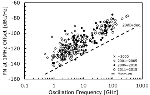
Figure 1 shows global conference publication data spanning 20 years (over 320 papers) relating to the depen- dence of the oscillation frequency on the phase noise of CMOS VCOs at 1-MHz offset from carrier frequency. As shown in Fig. 1, the lowest phase noise of 1-MHz offset from the carrier frequency in each oscillating frequency shows a dependence of approximately 20 dB/dec for the GHz oscil- lation frequency range.
The relationship between oscillation frequency and phase noise is well known as Leeson’s phase noise equa- tion[5], as shown in Eq. (1),
L(Δf)= 2kT F Posc
⎧⎪⎪⎨⎪⎪⎩1+ fosc
2QtankΔf 2⎫⎪⎪⎬
⎪⎪⎭
1+ f1/f
Δf
(1) where,Δf is the carrier offset frequency,kis the Boltzmann constant,T is the absolute temperature,Fis the noise factor of the gain cell, Posc is the root mean square value of the oscillation power, Qtank is the Q factor of the tank circuit, and f1/f is the flicker noise corner frequency.
As shown in Eq. (1), the theoretical frequency depen- dence of phase noise at a certain offset frequency should be 20 dB/dec. However, the lowest phase noise beyond K- and Ka-bands does not follow this 20 dB/dec line as shown in Fig. 1, and the possible reasons for this are considered to be among the following: F has been degraded by MOSFET’s channel noise enhancement due to scaling[6], f1/f has been degraded by MOSFET’s flicker noise enhancement[7],Posc
has been degraded by a fall in the power supply due to scal- ing, orQtankhas been degraded by high frequency operation.
Fig. 1 The global conference publication data spanning 20 years (over 320) relating to the dependence of the oscillation frequency on the phase noise of CMOS VCOs at 1-MHz offset from the carrier frequency.
Copyright c2016 The Institute of Electronics, Information and Communication Engineers
Fig. 2 Typical tank circuit of CMOS LC-VCO (a) and its equivalent cir- cuits (b).
In this study, we focus on the cause as the Q factor of the tank circuit degradation beyond K- and Ka-bands.
Figure 2 (a) shows a typical tank circuit using CMOS LC-VCO, which consists of a spiral inductor, a switched capacitor for course tuning, and a varactor for fine tuning;
the equivalent circuit is shown in Fig. 2 (b), where, Ltank, RL, Ctank, and RC are the inductance of the tank circuit, the series parasitic resistance of the inductor, the capaci- tance (which consists of the switched capacitors and the varactor), and the series parasitic resistance of capacitor, respectively.
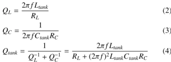
The Q factors of the inductor, QL, capacitor,QC, and tank circuit,Qtank, are shown in Eqs. (2) to (4).
QL=2πf Ltank
RL
(2) QC = 1
2πf CtankRC
(3) Qtank= 1
Q−1L +Q−1C = 2πf Ltank
RL+(2πf)2LtankCtankRC
(4) As shown in Eq. (4), Qtank depends on QL in the low fre- quency region but it depends onQC in the high frequency region, and therefore a number of researchers have stud- ied ways to improveQLbelow the 10 GHz region[8]–[11].
However, the most serious problem for Q factor degradation in K- and Ka-bands is caused byQC degradation. In this respect, we focused on an investigation ofQCof the varac- tor, and it was improved sevenfold at f =20 GHz in[12].
This improvement in QC provided a significant advantage for improvingQtank. Result, we need improvement of QL
in the K- and Ka-bands again. Therefore, this study focuses on the improvement ofQL. Overall strategy of our work is presented in Fig. 3.
This paper is organized as follows. Section 2 describes the skin effect and how to suppress Q factor degradation in the K- and Ka-bands using a striped inductor; Sect. 3 presents the design of the striped inductor and experiments relating to its utilizing of VCO; the measurements and sim- ulation results of inductors and VCOs are shown in Sect. 4;
and Sect. 5 concludes the results of this study.
Fig. 3 Overall strategy of our work to improve the Q factor of the tank circuit in the K- and Ka- bands.
2. Skin Effect in Inductor and Associated Method of Suppression
The skin effect of the spiral inductor occurs in the high- frequency region. The skin depth at a certain frequency,ds, is defined in Eq. (5) using resistivity, ρ, and permeability, μof metal[13]. Also, the surface current density, JS, and the normalized current density at certain depthx,JX, can be written in Eq. (6).
dS= ρ
πμf (5)
JX=JSe−dSx (6)
The current along the top and the bottom edge of the metal, IT, and the current along the left and the right edge of the metal,IW, are possible to be calculated by integratingJXas shown in Eqs. (7) and (8).
IT =2 T
2
0
JXdx=2JSdS
1−e−T/2dS
=JSTeff (7) IW =2
W2
0
JXdx=2JSdS
1−e−W/2dS
=JSWeff (8) where T is the total metal thickness, Teff is the effective metal thickness,W is the total metal width,Weff is the ef- fective metal width of the inductor.
Therefore,Teff andWeff, can be written in Eqs. (9) and (10).
Weff =2dS
1−e−W/2dS
(9) Teff =2dS
1−e−T/2dS
(10) Hence, the effective series resistance,RLeff, of the metal can be written in Eq. (11), wherelis the total metal length of the inductor.
RLeff =ρ l TeffW+WeffT
= πμρf
2 l
1−e−T/2dS W+
1−e−W/2dS T
(11)
inductor in the low frequency region,QLLF, and that in the high frequency region with the skin effect,QLHF, in the case ofWandT ds.
RLLF=ρ l
WT (12)
RLHF=RLeff ≈
πμρf l
2(W+T) (W,T dS) (13) QLLF=2πf LtankWT
ρl (14)
QLHF≈4πf LtankdS(W+T)
ρl =4Ltank(W+T) l
πf μρ
(15) Equations (12) and (13) show the frequency dependence of the inductor’s series resistance. It is evident that although there is zero dependence in the low frequency region, there is a square root dependence in the high frequency region.
From this series resistance frequency dependence, the fre- quency dependence of the Q factor in the low frequency re- gion is of a first order, but that in the high frequency region has a square root. In order to observe whether the skin effect occurs or not, the corner frequency of the skin effect is used as a parameter in Eq. (16).
fC=4 W+T
WT 2 ρ
πμ= 1
W + 1 T
2 ρ
πμ (16)
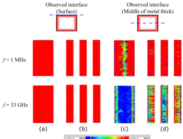
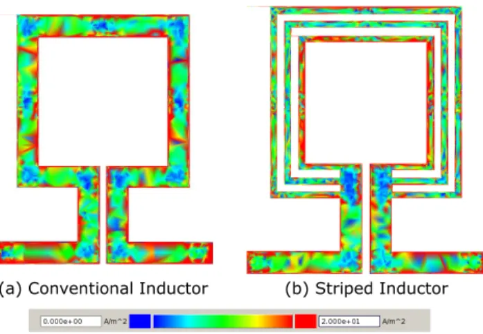
In the case of skin effect occurrence, the current flow in the inductor is concentrated on the peripheral of the metal line. We thus considered that it may be useful to expand the metal peripheral length to prevent series resistance enhance- ment due to the skin effect. One of the ideas behind metal peripheral length expansion is enlargement of metal line numbers with keeping total metal width. The 3D-electro- magnetic simulation results of current flow in a simple metal line and a striped metal line at f =1MHz and f =33 GHz are shown in Fig. 4. The thickness and the length of all metal line in Fig. 4 are 3.3μm and 200μm, and the width of the simple metal line is 7.5μm and the each width of the striped metal line is 2.5μm. The material of metal line was assumed copper. The relatively higher current density region is indi- cated by red and the relatively lower current density region is indicated by blue.
According to Fig. 4 (a) and (b), the current flow at the metal surface is constant for both the simple metal line and the striped metal line in any frequencies, however, the cur- rent flow in the metal line at the middle of the metal is not
Fig. 4 An observation of the current flow in a simple and a striped metal line at f =1 MHz andf =33 GHz by 3D-electro-magnetic simulation.
The simple metal line observed at surface, the striped metal line observed at surface, the simple metal line observed at middle of metal, and the striped metal line observed at middle of metal are shown in (a), (b), (c), and (d), respectively.
Fig. 5 Basic idea of proposed the striped inductor (b) and the conven- tional inductor (a).
concentrated in a relatively low frequency region such as f =1MHz, but is concentrated on the peripheral, even when the simple metal or the striped metal line is in a high fre- quency region such as f =33 GHz, as shown in Fig. 4 (c) and (d). It determined that, in the case of the striped metal line, the current flows on the peripheral of each stripe.
Therefore, the total current path of the striped metal line is approximately three times than that of the simple metal line.
Also, the current flow of the center of the striped metal line looks relatively low current density than that of the both side of the striped metal line. It seems influence of the proximity effect.
Using this phenomena, we thus proposed the striped in- ductor shown in Fig. 5[16]–[20]. In Fig. 5, the conventional and striped inductors are compared. The conventional in- ductor has one line of metal winding with a width ofW, and the striped inductor hasnstriped metal winding lines each width ofW/n, the total metal width of the striped inductor is identical to that of the conventional one. For the current flow
in the case of skin effect occurrence, the conventional induc- tor has four current paths, bottom, left, top and right which indicates that the peripheral length of the current path is 2W+2T, whereas the striped inductor has 4ncurrent paths, bottom, left, top and right of each stripe. As the metal width of the striped inductor is already divided byn, the periph- eral length of the current flow paths of the striped inductor is thus 2W/n(top and bottom of each stripe)×n+2T (left and right side of each stripe)×n =2W+2nT. This calcu- lation indicates that the striped inductor has 2(n−1)T paths more than the conventional inductor, and it is thus consid- ered hopeful that the series resistance of the striped inductor will be lower than that of the conventional one. In addition, it is hoped that the Q factor of the striped inductor will be larger than that of the conventional one.
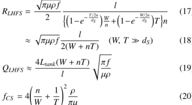
In consideration of this, the series resistance, Q factor, and corner frequency of the striped inductor,RLHFS,QLHFS, andfCS, are rewritten as Eqs. (17)–(20), respectively
RLHFS= πμρf
2 l
1−e−T/2ndS W
n+
1−e−W/2ndS T
n (17)
≈
πμρf l
2(W+nT) (W,T dS) (18) QLHFS≈4Ltank(W+nT)
l
πf
μρ (19)
fCS =4 n
W + 1 T
2 ρ
πμ (20)
However, in the case of the proximity effect occur- rence, the resistance of left and right side current paths of the metal will be large[9],[14],[15]. In this case,nwill be smaller than the divide number.
The characterization of the conventional and the striped inductors are summarized in Table 1.
Values of the series resistance of the striped inductor, RLHFS, the Q factor, QLHFS, and the corner frequency, fCS, can be obtained comparison with those of the conventional inductor according to Eqs. (13) and (18), (15) and (19), and (16) and (20).
RLHFS= W+T
W+nTRLHF (21)
Table 1 Summary of characterization of the conventional and the striped inductors and cross sectional current flow of them.
QLHFS= W+nT
W+T QLHF (22)
fCS =W+nT
W+T fC (23)
It is also considered that the following value of the phase noise from the striped inductor’s VCO, LS(Δf ), may be achieved, in comparison with the VCO of the conventional inductor as shown in Eq. (24).
LS(Δf)=
W+T W+nT
2
L(Δf) (24)
3. Inductor and VCO Design
To validate the performance of the striped inductor and the VCO utilizing it, a discrete inductor test pattern and a VCO test pattern utilizing both the conventional and striped in- ductors were designed. The details of the inductor are given in Fig. 6.
The conventional inductor designed had a square shape of D = 50μm and it consisted of one metal winding line withW =7.5μm. On the other hand, the designed striped inductor also had the same square shape (D =50μm), but it consisted of three metal winding lines with W=2.5μm, space, s = 2 μm. The metal structures of both inductors were M7 (Cu, T = 3.3 μm) and M8 (Al, T = 1.5 μm) stacked with a lot of vias. The calculated expected values of improvements in series resistance, Q factor and corner frequency of the striped inductor in comparison with the conventional inductor are 0.57, 1.68, and 1.68 times, respec- tively, using Eqs. (21)–(23).
In addition, three types of VCO pairs are designed to validate the performance of VCOs utilizing the striped in- ductor. Each pair of VCOs consists of a striped inductor VCO and a conventional inductor VCO. VCO-1 consists of a PMOS gain cell with inductors which shown in Fig. 6, VCO-2 consists of a NMOS gain cell with inductors which shown in Fig. 6, and VCO-3 consists of PMOS gain cell with similar shape inductors which shown in Fig. 6, but its induc- tor size isD=20μm. The estimated oscillation frequencies of VCO-1, VCO-2, and VCO-3 were 23, 25, and 40 GHz,
Fig. 6 Designed conventional inductor (a) and striped inductor (b) for experiments
Fig. 7 The equivalent circuit of designed PMOS-VCO (a) for VCO-1 and VCO-3, and NMOS-VCO (b) for VCO-2.
Table 2 Summary of designed VCOs.
respectively. The equivalent circuits of the VCOs are shown in Fig. 7, and the design of the VCO is summarized in Ta- ble 2.
The calculated expected value of improvements in phase noise for VCO is 5.0 dB, using Eq. (24).
4. Results and Discussion
In this section, the electro-magnetic simulation result of the discrete inductor, chip measurement results of the discrete inductor, and the chip measurement results of the VCOs are discussed. The test chip fabrication process used in this work is that of Toshiba 65-nm CMOS.
An observation of the current flow in the conventional and striped inductors at f = 33 GHz by using an electro- magnetic simulator is shown in Fig. 8, where the electro- magnetic simulator used was EMPro by Keysight Technol- ogy Inc. The current flow of both inductors is found to be concentrated in the peripheral of the metal lines. For the conventional inductor, the current flows in both sidewalls of the metal line, and for the striped inductor the current is flowing in both sidewalls of each metal line. Thus, the cur- rent paths of the sidewalls of the striped inductor are three times larger than that of the conventional inductor. This re- sult clearly illustrates the usefulness of the striped induc- tor. However, we were unable to obtain appropriate series resistances of the inductor at high frequency due to diffi- culties with mesh generation. But we could simulate series resistance at DC, and that of the conventional inductor was
Fig. 8 An observation of the current flow in the conventional and striped inductors at f=33 GHz by using an electro-magnetic simulator.
Fig. 9 The measured inductance, series resistance, and Q factor ofD= 50μm square shaped conventional and those of striped inductor.
0.18Ωand that of the striped inductor was 0.17Ω.
The discrete inductor test chip was measured using a PNA series vector network analyzer from Keysight Tech- nologies Inc. with an on-wafer probe station. The fre- quency range of the discrete inductor measurement was 1 to 67 GHz. The measureds-parameters were converted intoy- parameters, and they were then de-embedded using an open pattern. The inductance, series resistance, and Q factor were extracted fromy11[22].
The measured inductance, series resistance, and Q fac- tor of the 50-μm square shaped conventional inductor and the striped inductor are shown in Fig. 9. According to mea- surement results showed that, both inductors had similar in- ductance. However, the series resistance of the inductor was entirely different, that of the striped inductor was approxi- mately 0.7, 0.6, and 0.7 times that of the conventional one at f = 1, 10, and 25 GHz, respectively. In the case of f = 1 to 20 GHz, the measurement value is correspond- ing to the calculated value, but in the case of f >20 GHz, the measurement value is different a little from the calcu- lated value due to measurement unstableness or unexpected effect for instance the proximity effect. Furthermore, even in f =1 GHz, the skin effect occurs. The calculation value of the series resistance ratio at f = 1 GHz using Eqs. (11)
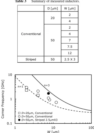
Table 3 Summary of measured inductors.
Fig. 10 The experimental results and calculated lines of corner frequen- cies of one-turn inductors withT =4.8μm and the calculated lines of corner frequency forn=1 and 3.
and (17) is 0.8. In addition, the Q factor of both inductor was also very different, that of the inductor was approx- imately 1.5 and 1.3 times larger than conventional one at f =15 GHz and 20 - 25 GHz, respectively. These measure- ment results show the advantage of using the striped induc- tor.
The corner frequency was determined using the Q fac- tor vs. frequency data. The merit of the corner frequency evaluation for characterization of the inductor is to elimi- nate the parasitic resistance influence in measurement, such as contact resistance by the on-wafer probe. Since parasitic resistance does not affect to the corner frequency extraction but it of course affects to the measured series resistance and absolute Q factor. To ensure the data, the corner frequencies of several inductors were determined, as shown in Table 3.
The experimental data relating to the metal width depen- dence of the corner frequency of one-turn inductors, and the calculated lines of corner frequencies are shown in Fig. 10, whereT =4.8 μm. Here, open circle denotes the conven- tional inductor withD = 50μm, open square denotes the conventional inductor with D = 20 μm, and closed circle denotes the striped inductor withD = 50μm. Moreover, the solid-and dashed lines denote the calculated corner fre- quency whenn=3 and 1, respectively.
Figure 10 shows that the experimental results and cal- culated lines of corner frequencies are consistent for both conventional and striped inductors. Furthermore, the cor-
ner frequency of the striped inductor is approximately 1.6 times higher than that of conventional inductor in the case ofW =7.5μm, and as a result, the striped inductor prevents degradation of Q factor of inductor. According to Fig. 10 and Eq. (20), the narrow metal width, the thin metal thick- ness and the large divide number are essential to obtain high corner frequency. However, the narrow metal width and the thin metal thickness cause higher series resistance as shown in Eq. (18), in other words, Q factor of inductor degrades us- ing the narrow metal or the thin metal. Therefore, large di- vide number is only solution to obtain high corner frequency and high Q factor.
The VCO test chip was measured using an EXA series signal analyzer by Keysight Technologies Inc. with an on- wafer probe station. The measurement data were corrected at an offset frequency of above 1 MHz to eliminate mea- sured phase noise offset due to AM modulation, because the measurement equipment was not able to cancel this above 1 MHz.
The measured phase noise as a function of the off- set frequency from the 23-GHz carrier of the VCO-1 uti- lizing conventional inductor and the striped inductor are shown in Fig. 11 (a), where the measurement condition was VDD = 1.2 V and the core current = 14 mA. The 1- MHz offset phase noise of the striped inductor’s VCO was
−105.9 dBc/Hz and that of the conventional inductor VCO was −102.3 dBc/Hz. As a result, the 1-MHz offset phase noise of the striped inductor’s VCO was exhibited 3.6 dB lower than that of the conventional inductor VCO. By con- trast, the estimated improvement of the phase noise of the striped inductor in the thermal noise region was 5.0 dB, as shown in Sect. 3. The cause of difference between the mea- sured value and the estimated value is considered as fol- lows. One is the effective metal of the current flowing is only M7. In that case, calculated phase noise improvement will be 4.1 dB. Another one is influence of the flicker noise up-conversion even at an offset frequency of 1-MHz since the corner frequency of the VCO’s flicker noise was approx- imately 600 kHz which was close from 1 MHz. Moreover, the influence of the proximity effect should be investigated since chip area is limited.
The measured phase noise as a function of the off- set frequency from the 25-GHz carrier of the VCO-2 uti- lizing conventional inductor and the striped inductor are shown in Fig. 11 (b), where the measurement condition was VDD = 1.2 V and the core current = 18 mA. The 1- MHz offset phase noise of the striped inductor’s VCO was
−102.3 dBc/Hz and that of the conventional inductor VCO was −99.8 dBc/Hz. As a result, the 1-MHz offset phase noise of the striped inductor’s VCO was exhibited 2.5 dB lower than that of the conventional inductor VCO. In VCO- 2, the flicker noise influence was more serious than VCO- 1 since the corner frequency of VCO was approximately 1 MHz. Hence, the phase noise improvement of the striped inductor’s VCO was compression.
The measured phase noise as a function of the off- set frequency from the 40-GHz carrier of the VCO-3 uti-
Fig. 11 The measured phase noise of VCO-1 (a), VCO-2 (b), and VCO- 3 (c) as a function of the offset frequency from the carrier frequency. The difference of the phase noise between the conventional inductor’s VCO and the striped inductor’s VCO is exhibited 3.6 dB for VCO-1, 2.5 dB for VCO- 2, and 3.7 dB for VCO-3, respectively, at 1-MHz offset from carrier.
lizing conventional inductor and the striped inductor are shown in Fig. 11 (c), where the measurement condition was VDD = 1.2 V and the core current = 24 mA. The 1- MHz offset phase noise of the striped inductor’s VCO was
−95.2 dBc/Hz and that of the conventional inductor VCO was −91.5 dBc/Hz. As a result, the 1-MHz offset phase noise of the striped inductor’s VCO was exhibited 3.7 dB lower than that of the conventional inductor VCO.
The 1-MHz offset phase noise was improved using the striped inductors for all the VCOs in these experiments in the K- and Ka-band frequency range. However, it is con- sidered that suppression of the flicker noise influence is requires.
Fig. 12 27 measured samples for the 1-MHz offset phase noise of VCO- 1. The closed circles show the phase noise of the striped inductor’s VCOs and the open circles show that of the conventional inductor’s VCOs.
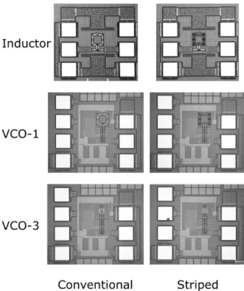
Fig. 13 Chip micro photograph of discrete inductors, VCO-1, and VCO- 3 utilized the conventional and striped inductor.
FOM= 1 L(Δf)
fOSC
Δf 2
1 PDC
Table 4 compares this study with state-of-the-work K- and Ka-bands VCOs.
Several chips were measured to validate phase noise improvement using the striped inductor. Figure 12 shows
27 measured samples for the 1-MHz offset phase noise of VCO-1, in which the closed circles represent the striped inductor VCOs and open circles those of the conventional inductor. There are variations in the differences between the phase noise of the striped inductor VCOs and that of con- ventional inductor, but Fig. 12 shows the evident advantage of using the striped inductor.
Figure 13 shows chip micro photographs of the dis- crete inductors of both the conventional and striped inductor, and that of VCO-1 and VCO-3 utilized the conventional and striped inductor.
5. Conclusion
A striped inductor and its utilization of VCO were studied the aim of suppressing phase noise degradation in K- and Ka-bands. Results showed that the Q factor at f =25 GHz and the corner frequency of the striped inductor were ap- proximately 1.3 and 1.6 times higher, respectively, than that of the conventional inductor. In addition, the 1-MHz-offset phase noise of the VCO of the striped inductor in K- and Ka-bands approximately 3.5 dB lower than that of the con- ventional inductor. These results indicate that the proposed striped inductor exhibited reduced series resistance in the high frequency region by preventing the skin effect. How- ever, it is evident that future studies are required to inves- tigate the current flowing paths in the case of the stacked metal and the influence of the proximity effect. In this study, 65-nm standard CMOS process was used.
Acknowledgments
This work was supported by JSPS KAKENHI Grant Num- ber 25420338. Also, this work was supported by VLSI Design and Education Center (VDEC), the University of Tokyo in collaboration with Cadence Design Systems, Inc.
and Keysight Technologies Japan, Ltd.
References
[1] C.E. Shannon, “A Mathematical Theory of Communication,” The Bell System Technical Journal, vol.27, no.3, pp.379–423, July 1948.
[2] A. Mazzanti, M. Sosio, M. Repossi, and F. Svelto, “A 24GHz sub- harmonic receiver front-end with integrated multi-phase LO genera- tion in 65nm CMOS,” ISSCC 2008, vol.51, pp.216–217, Feb. 2008.
[3] K. Okada, K. Kondou, M. Miyahara, M. Shinagawa, H. Asada, R. Minami, T. Yamaguchi, A. Musa, Y. Tsukui, Y. Asakura, S.
Tamonoki, H. Yamagishi, Y. Hino, T. Sato, H. Sakaguchi, N.
Shimasaki, T. Ito, Y. Takeuchi, N. Li, Q. Bu, R. Murakami, K. Bunsen, K. Matsushita, M. Noda, and A. Matsuzawa,
“Full Four-Channel 6.3-Gb/s 60-GHz CMOS Transceiver with Low-Power Analog and Digital Baseband Circuitry,” IEEE J.
Solid-State Circuits, vol.48, no.1, pp.46–65, Jan. 2013.
[4] K. Katayama, M. Motoyoshi, K. Takano, N. Ono, and M. Fujishima,
“28mW 10Gbps Transmitter for 120GHz ASK Transceiver,” IMS, pp.1–3, June 2012.
[5] D.B. Leeson, “A simple model of feedback oscillator noise spec- trum,” Proc. IEEE, vol.54, no.2, pp.329–330, Feb. 1966.
[6] N. Itoh, K. Kojima, and T. Ohguro, “Channel Noise Enhancement
in Small Geometry MOSEFT and Its Influence on Phase Noise Cal- culation of Integrated Voltage-Controlled-Oscillator,” International Journal of Numerical Modelling, vol.18, no.4, pp.255–266, John Wiley & Sons, July 2005.
[7] H. Kimijima, T. Ohguro, B. Evans, B. Acker, J. Bloom, H. Mabuchi, K. Dim-Lee, E. Morifui, T. Yoshitomi, H.S. Momose, M. Kinugawa, Y. Katsumata, and H. Iwai, “Improvement of 1/f noise by using VHP (Vertical High Pressure) oxynitridegate insulator for deep-sub mi- cron RF and analog CMOS,” Symp. VLSI Tech. Dig., pp.119–120, Kyoto, 1999.
[8] C.P. Yue and S.S. Wong, “Physical Modeling of Spiral Inductors on Silicon,” IEEE Trans. Electron Devices, vol.47, no.3, pp.560–568, March 2000.
[9] Y. Cao, R.A. Groves, X. Huang, N.D. Zamdmer, J.-O. Plouchart, R.A. Wachnik, T.-J. King, and C. Hu, “Frequency-Independent Equivalent-Circuit Model for On-Chip Spiral Inductors,” IEEE J.
Solid-State Circuits, vol.38, no.3, pp.419–426, March 2003.
[10] C.B. Sia, K.S. Yeo, M.A. Do, and J.-G. Ma, “Metallization Prox- imity Studies for Copper Spiral Inductors on Silicon,” IEEE Trans.
Semicond. Manuf., vol.16, no.2, pp.220–227, May 2003.
[11] J.M. Lopez-Villegas, J. Samitier, C. Cane, P. Losantos, and J.
Bausells, “Improvement of the Quality Factor of RF Integrated Inductors by Layout Optimization,” IEEE Trans. Microw. Theory Techn., vol.48, no.1, pp.76–83, Jan. 2000.
[12] Y. Itano, S. Morimoto, S. Yoshitomi, and N. Itoh, “High-Q MOS Varactor Models for Quasi-Millimeter-Wave Low-Noise LC-V- COs,” IEICE Trans. Fundamentals, vol.E97-A, no.3, pp.759–767, March 2014.
[13] F.W. Grover, Inductance Calculations, Dover Publications, ISBN- 13:978-0-486-47440-3, 1946.
[14] R.-J. Chan and J.-C. Guo, “Analysis and Modeling of Skin and Prox- imity Effects for Millimeter-Wave Inductors Design in Nanoscale Si CMOS,” Proc. 9th European Microwave Integrated Circuits Confer- ence, pp.13–16, Oct. 2014.
[15] X. Nan and C.R. Sullivan, “An Improved Calculation of Proximi- ty-Effect Loss in High-Frequency Windings of Round Conductors,”
IEEE 34th Annual Power Electronics Specialist Conference, vol.2, pp.853–860, June 2003.
[16] N. Itoh, Y. Itano, S. Morimoto, and S. Yoshitomi, “Striped Induc- tor for Quasi Millimeter Wave Voltage-Controlled Oscillator,” Proc.
Asia-Pacific Microwave Conference, pp.319–321, Seoul, Nov. 2013.
[17] H. Tsuji, Y. Itano, K. Komoku, T. Morishita, S. Yoshitomi, and N.
Itoh, “Millimeter-Wave VCO using Striped Inductor,” Proc. Asia- Pacific Microwave Conference 2014, pp.959–961, Sendai, Nov.
2014.
[18] N. Itoh, Y. Itano, H. Tsuji, K. Komoku, T. Morishita, and S.
Yoshitomi, “A Study of enhancement of Q-factor of LC Resonators in high frequency region,” IEICE Technical Report, ICD2014-24, July 2014.
[19] N. Itoh, H. Tsuji, Y. Itano, K. Komoku, T. Morishita, and S.
Yoshitomi, “A Study of High-Frequency Characteristics of Stripe Shaped Inductor and its Application for Voltage-Controlled Os- cillator,” IEICE Technical Report, EMCJ2015-74, MW2015-113, EST2015-84, Oct. 2015.
[20] H. Tsuji, Y. Itano, K. Komoku, T. Morishita, S. Yoshitomi, and N.
Itoh, “A Study of Flicker Noise Suppression of K-Band VCO using Striped Inductor,” Proc. Asia-Pacific Microwave Conference 2015, WE4E-1, Nanjing, Dec. 2015.
[21] O. Richard, A. Siligaris, F. Badets, C. Dehos, C. Dufis, P. Busson, P. Vincent, D. Belot, and P. Urard, “A 17.5-to-20.94GHz and 35-to-41.88GHz PLL in 65nm CMOS for Wireless HD Applica- tions,” ISSCC 2010, vol.53, pp.252–253, Feb. 2010.
[22] S. Yoshitomi, “Analysis and simulation of spiral inductor fabricated on silicon substrate,” Proc. 2004 11th IEEE International Confer- ence on Electronics, Circuits and Systems, pp.365–368, Dec. 2004.
He had been a Visiting Scientist at Katholieke Universiteit Leuven, ESAT- MICAS, Leuven, Belgium, from 1996 to 1998, where he had worked on design of fully integrated VCOs and PLLs using RFCMOS. He has been engaged in the research and development of high-frequency analog circuit at Semiconductor Company of Toshiba Corporation since 1998. He was also a part-time lecturer of Chuo University, Tokyo, Japan, since 2009.
Since 2010, he has been full time professor of Okayama Prefectural Uni- versity. His current research interests are high-frequency integrated circuit for telecommunications. Dr. Itoh is a member of IEEE and also senior member of IEICE. He received the Asia-Pacific Microwave Conference (APMC) Prize in 2007. He has been a member of TPC of CICC, BCTM, ESSCIRC, TJMW, and RFIC symposium, was a secretary of IEEE MTT-S Japan Chapter, was the Publicity Chair of APMC 2010, and was a secretary of URSI-C Japan Committee.
Hiroki Tsuji received the B.E. degree from Okayama Prefectural University, Soja, Japan, in 2014. He is currently pursuing M.E. at Okayama Prefectural University, Soja, Japan.
His current research interests are high-frequency integrated circuit for telecommunications.
Yuka Itano received the B.S. and M.S degrees in physics from Nara Women’s Uni- versity, Nara, Japan in 2006 and 2008, respec- tively. In 2008, she joined Semiconductor Mass Storage Company, Toshiba Corporation, Kawa- saki, Japan, where she was engaged in Analog Device Design Engineering Group Analog &
Imaging Sensor Division. She is currently pur- suing Ph.D. at Okayama Prefectural University, Soja, Japan.
Takayuki Morishita received the B.S., M.S.
and Ph.D. degrees in electronics from Okayama University, Okayama, Japan, in 1979, 1981 and 1988, respectively. In April 1993, he joined the Department of Communication Engineering at Okayama Prefectural University, as an associate professor. His current research interests are re- configurable microprocessors and VLSI design.
Sadayuki Yoshitomi received the B.E.
and M.E, and Ph.D. degrees from Yokohama National University, Yokohama, Japan, 1988, 1990, and 1993, respectively. His title of his doctor thesis was “The study on the silicon dioxide film deposited by liquid phase deposi- tion (LPD)”. His background is the physics of Si/SiO2 interface. In 1993, he joined the Re- search and Development Center, Toshiba Cor- poration, Kawasaki, Japan, where he is currently engaged in the development of design infras- tructures of analog and RF CMOS and BiCMOS process technology. He has been a member of TPC of MIXDES, and an organizing committee of MOS-AK/GSA (Global Semiconductor Alliance).