SUMMARY In this paper, we evaluate a prediction method of regions including dislocation clusters which are crystallographic defects in a pho-toluminescence (PL) image of multicrystalline silicon wafers. We applied a method of a transfer learning of the convolutional neural network to solve this task. For an input of a sub-region image of a whole PL image, the net-work outputs the dislocation cluster regions are included in the upper wafer image or not. A network learned using image in lower wafers of the bottom of dislocation clusters as positive examples. We experimented under three conditions as negative examples; image of some depth wafer, randomly se-lected images, and both images. We examined performances of accuracies and Youden’s J statistics under 2 cases; predictions of occurrences of dis-location clusters at 10 upper wafer or 20 upper wafer. Results present that values of accuracies and values of Youden’s J are not so high, but they are higher results than ones of bag of features (visual words) method. For our purpose to find occurrences dislocation clusters in upper wafers from the input wafer, we obtained results that randomly select condition as negative examples is appropriate for 10 upper wafers prediction, since its results are better than other negative examples conditions, consistently.
key words: prediction, transfer learning, convolutional neural network
1. Introduction
Technologies for manufacturing high-quality silicon wafers for solar cells are being intensively developed, and a novel crystal growth technique has been pursued to permit real-ization of a high-quality multicrystalline silicon ingot while keeping its advantage of simple directional solidification in a crucible to result in high production yield and low cost. In fact, nucleation control at the bottom of the crucible was recognized as a useful method to control the size of crystal grains in the order of a few mm, leading to reduction of the dislocation density. However, dislocation clusters in mul-ticrystalline silicon wafers still remain as one of the main crystal defects to reduce the conversion efficiency of solar
Manuscript received June 30, 2020. Manuscript revised October 22, 2020. Manuscript publicized December 8, 2020.
†
The authors are with the Graduate School of Informatics, Na-goya University, NaNa-goya-shi, 464-8601 Japan.
††
The author is with the Center for Advanced Intelligence Project, RIKEN, Tokyo, 103-0027 Japan.
†††
The author is with the Graduate School of Engineering, Na-goya University, NaNa-goya-shi, 464-8603 Japan.
∗
This paper is an extended version of a manuscript that was presented in the 10th International Workshop on Image Media Quality and its Applications (IMQA2020)[16]with additional de-scriptions.
a) E-mail: [email protected] DOI: 10.1587/transfun.2020IMP0010
cells. For further improvement of the crystal quality of the multicrystalline silicon ingot, we need to somehow suppress the generation of dislocation clusters during crystal growth based on the knowledge of their generating mechanism.
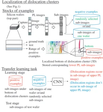
We can observe many grains or ‘small regions with different textures’ (see Fig. 5) in a multicrystalline silicon wafer. Occurrences of dislocations are affected by crystallo-graphic orientations between neighboring grains, and affect an electrical performance as solar cells. Dislocation clus-ters in a silicon wafer are invisible with the naked eye, how-ever, we can observe them in a photoluminescence(PL) im-age which is a particular imim-age.
A PL image records emission lights captured by an in-frared camera under an illuminant of a laser light. Dislo-cations clusters are recorded as dark regions in the image. From this, we can guess dislocations lead a low efficiency as solar cells. We are seeking to clarify to a generating mecha-nism of dislocation clusters to decrease occurrences of them. At first, we implemented a software that extracts regions of dislocation clusters in a PL image for each sliced wafer in a multicrystalline silicon ingot, and traces regions from bot-tom to top. We presented the method on visualizing the 3D structures of an evolution of dislocation clusters in a silicon ingot[1]as Fig. 1. The right figure shows the result using wafers from #611 to #868. In a manufacturing process, a multicrystalline silicon ingot is formed by a solidification at the bottom to top in cooling process. In this process, dislo-cation clusters generate and growth up and shrink.
With this method, we extracted regions of the bottom of dislocation clusters in an silicon ingot to identify a gen-eration point of a dislocation cluster. However, a certain degree of dislocation clusters are required to be recorded as a dark pixel in a PL image. Therefore, a true generation point of a dislocation cluster may exist in lower wafers. We attempted to detect them by more accurate method[2]. We applied detection algorithm to a micro-PL image instead of a (macro-)PL image, and traced dislocation regions. A micro-PL image is a high-resolution image for a smaller area.
However, if we can realize a prediction of candidate ar-eas which includes a true generation point in lower wafer (macro-)PL images, it is useful. We implemented an al-gorithm based on the image processing to extract disloca-tion regions in[1]. Next, we introduced a machine learning method to specify them. We tried a matrix decomposition Copyright c 2021 The Institute of Electronics, Information and Communication Engineers
Fig. 1 3D visualization of dislocations clusters.
method which calculates from a matrix presents pixel in-tensities of sub-images in a PL image to matrixes express feature images and its coefficients. We applied an algorithm of a dictionary learning framework in a broad sense. Fea-ture images are obtained by independent component analy-sis and non-negative matrix factorization(NMF)[3]for PL sub-images. NMF is used as a modeling method for a phys-ical phenomenon. For example, it is used as a sound separa-tion algorithm for a power-spectrogram[4],[5], it decom-poses a matrix of the spectrogram into an activation ma-trix and a spectrum mama-trix. Since an activation mama-trix is corresponding to a ratio of mixed signals, non-negative is adequate. A spectrum matrix expressed power-spectrum is non-negative, originally. Similarly, parts of an object are separated from an image by an approach of NMF[6],[7]. The values of both mixed ratio and pixel intensities of an image takes non-negative values. As dislocation regions are small part in a wafer, we considered a most of feature im-ages reflect on lots of regions which do not include disloca-tions. Therefore, regions which include dislocation clusters are extracted according to a criterion that a difference be-tween a reconstruction image calculated by feature images and its coefficients and the original image is large.
Recently, deep neural networks are applied to current practical tasks on a defect detection of solar cells[8],[9]. Defects in these researches are not meant for the same of crystal defects in a silicon wafer as materials in our task, but be a physical damages such as e.g., micro-cracks in the stage of a product testing. The crystal defects of dislocation clusters are not results that occurred by temporal changes in the future as we see in Fig. 1. Before we tried to apply a transfer learning of a convolutional neural network (CNN) to detect the crystal defects, we introduced the multilayer perception (MLP) for the task [10]as a method by a su-pervised learning. We tried to change the numbers of
hid-Fig. 2 Outline of proposed method.
den layers to embed processes of image features extraction and classification. We expected to improve the performance of classification of images, because the network could uti-lize information of supervised data. However, it performed similar or worse results of NMF as a kind of unsupervised methods. Values of Youden’s J described in Sect. 3.2 were obtained about 0.3 for MLP and about 0.3 to 0.7 for NMF. Therefore, we focused on a transfer learning of a convolu-tional neural network (CNN). As a task of[11], a network classifies an image to a category which includes dislocation regions or a category which does not include dislocation re-gions from example images of both classes. The network has feed-forward structures, and it learns by supervised-learning method. As a transfer supervised-learning, weights of the net-work is assigned by weights of a pre-trained convolutional neural network (AlexNet[12]). The last layer of its network was replaced by output cells and learned their weights for the task of a dislocation region detection. We experimented and confirmed the performance of this network. We con-sidered a transfer learning framework was appropriate for special uses images or a defect detection task[13], since the number of positive examples are small, relatively. Disloca-tion clusters regions are only a little in a whole silicon wafer image. Values of Youden’s J were obtained similar to values for NMF.
Figure 2 shows the outline of proposed method. In this paper†, we tried to apply a framework of transfer learning
of CNN to predict a generation of dislocation clusters in the upper PL images. In Sect. 2, we explain structures of a net-work and the prediction task. In Sect. 3, we explain
exper-†
This paper is an extended version of the manuscript of IMQA2020[16].
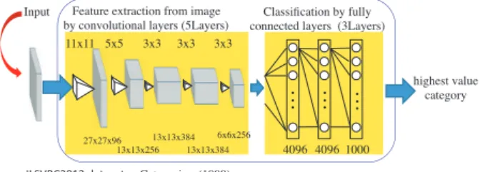
We used AlexNet[12]as a pre-trained convolutional neu-ral network. As an input to the network, a color image (227×227 pixels, RGB-3 channels) is used. The network outputs one category from 1,000 general image categories.
Figure 3 shows structures of AlexNet. It has 5 con-volution layers and 3 fully connected layers. Concon-volution layer has kernels (or channels, for example, 3 channels in the input layer). A kernel is consisted of 2 dimensional array elements. It works as a filter in image processing. Weights of the network are calculated at the values which were pre-trained by an image classification task of ILSVRC (ImageNet large scale visual recognition challenge).
The 1st, 2nd, and 5th convolution layers process con-volution, activation function (Rectified Linear Unit; ReLU), normalization, and max pooling operations. The 3rd and 4th layers process convolution, activation function (ReLU), and normalization operations. The 1st and 2nd fully connected layers process full connection, activation function (ReLU), and dropout operations. The last fully connected layer has full connections, and performs softmax operations to output the one category from 1,000 categories. To see more con-cretely, the 1st convolution layer operates convolution by filter of size by 11×11 with strides 4×4. It is consisted of 96 kernels. One kernel is composed with a 2-dimensional array by 55×55 elements. After this, max pooling process is done by a filter of size 3×3 with strides 2×2. Finally, 96 ker-nels which are composed a 2-dimensional array by 27×27 elements were created. The remain convolution layers are perform a similar processes. The 1st and 2nd fully con-nected layers have weighted connection, and some connec-tions among them were deleted (dropout), randomly. Here, a rate of a dropout was set to 50%.
As a transfer learning, our network kept weights of these connections. These layers work as a feature extractor of an input image. We changed a connection structure of the last full connected layer to classify from 1,000 categories to 2 categories. Two classes correspond to categories whether an input sub-image of a PL image includes dislocation re-gions in upper wafers or not. Loss function was defined by a calculation of cross-entropies.
In [11], the network outputs one of categories of whether an input image including dislocation clusters or not, for a sub-image of a silicon wafer PL image, directly. To
Example images are collected by identifying a location of the bottom of dislocation clusters and extract further lower 10 or 20 images at the same location in lower wafer. The bottom image of dislocation clusters has very small region as dislocation features. Therefore, lower images are not able to discriminate other conventional region images well. As a technical point, the originated network of transfer learn-ing, that is, AlexNet is trained by a large size which is com-pared to our input image size, and color image, and natural scenes. On the other hands, the input images (16×16 pixels) are small because we do not identify a silicon wafer which include defects or not, but we identify to locate dislocations regions in a wafer image. And, input images are gray-scale format and ’un-natural scene’ or texture images which are far from the training data set. Therefore, we consider that showing results to apply the transfer learning to our tasks is useful for the similar task which uses such special images. In addition, since we show the performance under the con-ditions with using 10 or 20 wafers as positive examples of learning data, it will have a worth to estimate the numbers or how to select examples for prediction tasks.
We used PL images of sliced wafers from one mul-ticrystalline silicon block. Dimensions of a wafer are 156×156 mm, and thickness is 180 µm. A sliced pitch is 290 µm, we can convert from the number of a wafer to a physical height in a silicon block with this value of the sliced pitch. We assigned an index for each wafer from bottom wafer to top wafer in silicon block. A PL image is a gray-scaled image. We set exposure duration to 2 sec under the condition of laser output 80 W (λ=940 nm). In the Fig. 4, we showed a wafer number to use in this paper. The bottom and top wafer is #1 and #868 in a silicon ingot, respectively. The upper part (#611 to #868) in a silicon block which includes lots of dislocation clusters than the lower part is a range of the subject of this paper. Positive examples are extracted from #631 to #680 wafers. Negative examples are extracted from randomly selected from upper part (#611 to #857) or #611 wafer. Input images of a network are segmented im-ages from #751 wafer, regularly. A ground truth is made by identifying regions of the occurrences of dislocation clus-ters in #761 wafer as the same location of an input image of #751 for a condition using the positive examples of 10 wafers. Similarly, the ground truth of #771 are defined for a condition using the positive examples of 20 wafers.
Fig. 4 Wafer properties.
Fig. 5 PL image (#751); red regions present dislocation clusters candi-dates extracted by image processing[16].
Dislocation clusters whose height has more than 10 wafers are extracted by an image processing procedure are traced and identify the bottom of its clusters. As a possi-ble generation point of dislocation clusters, we stored 10 or 20 images at the same location in lower wafers. To say inversely, the image is a example that it occurs dislocation clusters at the same location within upper 10 or 20 wafers. These are positive examples.
On the other hand, negative examples that are collected by three conditions; 961 images from #611 (the bottom of our treated PL images in this report), 900 images from ran-dom selection, and total images of both conditions.
Test images are sampled as sub-image of #751 wafer. Figure 5 shows a PL image of #751 wafer, and red col-ored regions present extracted regions by image processing as dislocation clusters. This is an enhancement contrasted image after image processing to reduce sliced-marks which are occurred by cutting out wafers from a silicon block[1]. Figure 6 shows examples of (a) images which include dis-location clusters training set, (b) images in #611 wafer, (c) randomly selected images.
Python programs and OpenCV libraries were used to
Fig. 6 Examples of positive and negative examples[16].
implement these operations on Windows PC. 3. Experiment
3.1 Input Images and Ground Truth
We segmented an enhanced PL image (500×500 pixels) into sub-regions whose size is 16×16 pixels. A PL image is di-vided into 31×31 regions as sub-images. 4 pixels regions of right-end and bottom-end were not used. It corresponds to cropping a PL image of a size of 496×496 pixels. AlexNet accepts a color image as an input image. In program, a sub-image of a PL sub-image was converted to a color format sub-image. A ground truth image was defined by a unit of a sub-region (16×16 pixels) by a handwork for image processing results for #751, #761, and #771 wafers. We defined the ground truth as manually, since the identification of regions of the occurrences of dislocation clusters in #761 or #771 which are 10 or 20 upper wafers of a test wafer (#751) is easy to judge whether a segmented area which corresponds to the input image include red-colored pixels by a method [1]in the image like Fig. 5 or not. The number of regions which include dislocations are 152, 165, and 160 for #751, #761, and #771 wafers, respectively. They are not corresponding to the number of dislocation clusters, because that is a com-mon case that one cluster is included in some sub-images.
Image augmented processes of image-shift and flip are performed by inside processes in a program. MATLAB R2018b/R2019b program was used to implement transfer learning on a windows PC (Windows 10 Pro, Intel Core i9-7900X, 32 Gbyte, GPU: NVIDIA Quadro P5000).
3.2 Results
Fig. 7 Example of prediction results on #761 wafer image (10 wafers, 10 epochs, random); green TP, blue FN, yellow FP, no-mark TN.
upper wafers and compared them to results of other method, that is, bag of features (visual words), and examined ef-fects by differences of negative examples. We set mini-batch size at 16. We trained a network in 10, 30, 50, 100 and 200 epochs for training data. Epoch represents the number of displaying turns of all data. 5 trials are performed for each condition. Figure 7 shows an example of prediction results of dislocation regions overlapped on the image of #761 wafer. It shows results of the condition of 10 wafers, 10 epochs, and randomly selected images as negative exam-ples. Green squares correspond to true positive (TP) regions of 78. Blue ones do to false negative (FN) regions of 87. Yellow ones do to false positive (FP) regions of 180. No marked regions do to true negative (TN) regions of 616. In this example, statistics of accuracy and Youden’s J are 0.722 and 0.247, respectively.
We calculated accuracies of predictions. Accuracy = TP+ TN
TP+ TN + FP + FN
We also calculated Youden’s J statistic[14]. Youden’s J is a performance index which is calculated from a sensitiv-ity (TP)/(TP+FN) and a specificity (TN)/(TN+FP). These measures are corresponding to each axis of the ROC (Re-ceiver operating characteristic) curve taking as the value of (1- specificity). J= Sensitivity − (1 − Specificity) = Sensitivity + Specificity − 1 = TP TP+ FN+ TN TN+ FP− 1 3.2.1 20 Wafers Results
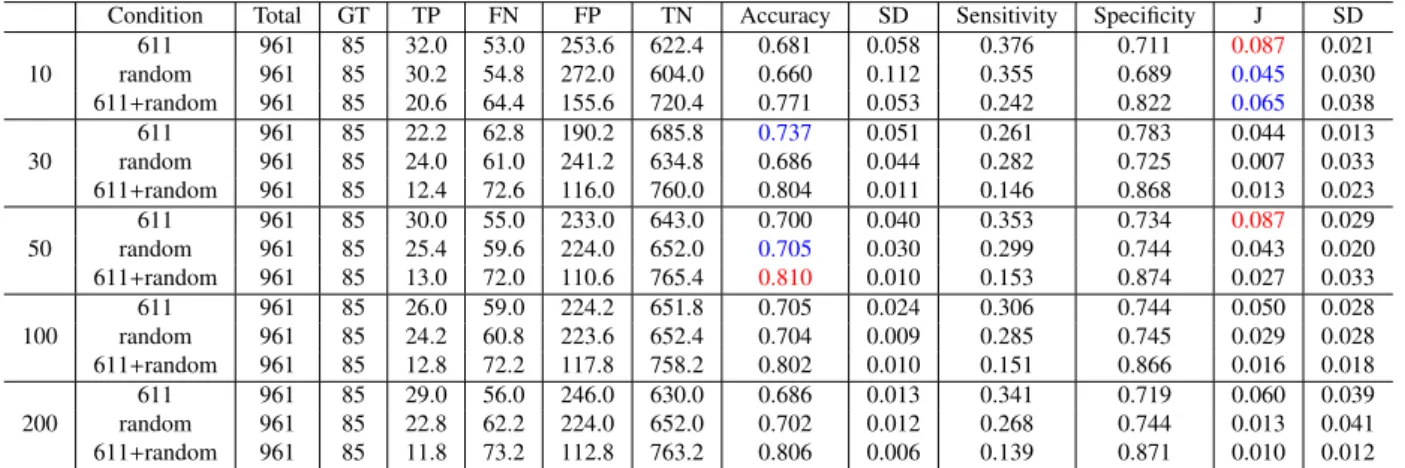
Tables 1 and 2 show results in negative examples conditions (611, random, and 611+random) for a prediction for upper 20 wafers when #751 wafer was used as an input. Table 1
ber of ground truth and sample standard deviation for values of accuracy or Youden’s J. The best values show by the col-ored(red/blue) fonts for each negative example condition for values of accuracy and Youden’s J. And, red colored values mean the best in all conditions.
We compared them to results of a prediction based on an algorithm of bag of features (visual words)[15]with the same dataset. We show results in Tables 3 and 4. The best values are shown by red colored fonts.
For a learning stage, accuracies and Youden’s J reached at 1 of a theoretical best value at least 50 epochs condition in these trials. For a test stage, values of sample standard de-viation of accuracy show smaller according to increase the number of epochs in Tables 1 and 2 for any negative example conditions. Accuracies take values about 0.65 to 0.75 and 0.65 to 0.80, respectively. These values are higher than re-sults about 0.65 of bag of features (visual words) in Tables 3 and 4. Especially, 611+random conditions are better than other negative example conditions. Values of 611+random condition take higher than other conditions. In this experi-ment, we added example images of both conditions, simply. Therefore, the number of examples are increased, it is rea-sonable to improve performances. Values in Table 2 reached about 0.8.
However, sensitivities take low scores. Therefore, the higher rate is obtained by improving to increase a correct rate for true negative images. In our purpose, to improve for true positive image is more interest as a meaningful predic-tion. Therefore, it is thought that Youden J statistics is more important to present for a performance of predictions. Max-imum values of Youden’s J are obtained from 611+random condition in Table 1 and 611 condition in Table 2. However, scores of Youden’s J are low about 0.1. Since Youden’s J in results of bag of features are about 0, the results are better than one of bag of features, at least.
To compare between results in Tables 1 and 2, the best value of accuracies is obtained in Table 2 from the view of an occurrence prediction of dislocation clusters. This means a condition excluding images that dislocation clusters has occurred already in an input image is better, although such regions images are not given as examples. The best value of Youden’s J degrades low scores in this condition, and 10 epochs result are better than more repeated epochs results.
Table 1 Result of occurrence prediction of 20 upper wafers for #751 wafer input (Dislocation in #771 wafer).
Condition Total GT TP FN FP TN Accuracy SD Sensitivity Specificity J SD
611 961 160 61.0 99.0 224.6 576.4 0.663 0.049 0.381 0.720 0.101 0.033 10 random 961 160 65.0 95.0 237.2 563.8 0.654 0.087 0.406 0.704 0.110 0.021 611+random 961 160 44.6 115.4 131.6 669.4 0.743 0.041 0.279 0.836 0.114 0.010 611 961 160 45.0 115.0 167.4 633.6 0.706 0.032 0.281 0.791 0.072 0.042 30 random 961 160 54.8 105.2 210.4 590.6 0.672 0.039 0.343 0.737 0.080 0.033 611+random 961 160 31.6 128.4 96.8 704.2 0.766 0.008 0.198 0.879 0.077 0.025 611 961 160 58.8 101.2 204.2 596.8 0.682 0.035 0.368 0.745 0.113 0.026 50 random 961 160 55.6 104.4 193.8 607.2 0.690 0.020 0.348 0.758 0.106 0.022 611+random 961 160 30.0 130.0 93.6 707.4 0.767 0.004 0.188 0.883 0.071 0.018 611 961 160 52.4 107.6 197.8 603.2 0.682 0.021 0.328 0.753 0.081 0.026 100 random 961 160 55.2 104.8 192.6 608.4 0.691 0.010 0.345 0.760 0.105 0.040 611+random 961 160 32.0 128.0 98.6 702.4 0.764 0.009 0.200 0.877 0.077 0.010 611 961 160 58.2 101.8 216.8 584.2 0.668 0.008 0.364 0.729 0.093 0.016 200 random 961 160 51.6 108.4 195.2 605.8 0.684 0.009 0.323 0.756 0.079 0.022 611+random 961 160 29.4 130.6 95.2 705.8 0.765 0.007 0.184 0.881 0.065 0.028
Table 2 Result of occurrence prediction of 20 upper wafers for #751 wafer input (Dislocation in #771 wafer, not dislocation in #751).
Condition Total GT TP FN FP TN Accuracy SD Sensitivity Specificity J SD
611 961 85 32.0 53.0 253.6 622.4 0.681 0.058 0.376 0.711 0.087 0.021 10 random 961 85 30.2 54.8 272.0 604.0 0.660 0.112 0.355 0.689 0.045 0.030 611+random 961 85 20.6 64.4 155.6 720.4 0.771 0.053 0.242 0.822 0.065 0.038 611 961 85 22.2 62.8 190.2 685.8 0.737 0.051 0.261 0.783 0.044 0.013 30 random 961 85 24.0 61.0 241.2 634.8 0.686 0.044 0.282 0.725 0.007 0.033 611+random 961 85 12.4 72.6 116.0 760.0 0.804 0.011 0.146 0.868 0.013 0.023 611 961 85 30.0 55.0 233.0 643.0 0.700 0.040 0.353 0.734 0.087 0.029 50 random 961 85 25.4 59.6 224.0 652.0 0.705 0.030 0.299 0.744 0.043 0.020 611+random 961 85 13.0 72.0 110.6 765.4 0.810 0.010 0.153 0.874 0.027 0.033 611 961 85 26.0 59.0 224.2 651.8 0.705 0.024 0.306 0.744 0.050 0.028 100 random 961 85 24.2 60.8 223.6 652.4 0.704 0.009 0.285 0.745 0.029 0.028 611+random 961 85 12.8 72.2 117.8 758.2 0.802 0.010 0.151 0.866 0.016 0.018 611 961 85 29.0 56.0 246.0 630.0 0.686 0.013 0.341 0.719 0.060 0.039 200 random 961 85 22.8 62.2 224.0 652.0 0.702 0.012 0.268 0.744 0.013 0.041 611+random 961 85 11.8 73.2 112.8 763.2 0.806 0.006 0.139 0.871 0.010 0.012
Table 3 Result of occurrence prediction of 20 upper wafers for #751 wafer input (Dislocation in #771 wafer) (Bag of features).
Condition Total GT TP FN FP TN Accuracy SD Sensitivity Specificity J SD
611 961 160 53.8 106.2 253.6 547.4 0.626 0.009 0.336 0.683 0.020 0.036
BOF random 961 160 51.6 108.4 244.2 556.8 0.633 0.019 0.323 0.695 0.018 0.044
611+random 961 160 50.4 109.6 233.4 567.6 0.643 0.007 0.315 0.709 0.024 0.025
Table 4 Result of occurrence prediction of 20 upper wafers for #751 wafer input (Dislocation in #771 wafer, not dislocation in #751) (Bag of features).
Condition Total GT TP FN FP TN Accuracy SD Sensitivity Specificity J SD
611 961 85 27.8 57.2 279.6 596.4 0.650 0.008 0.327 0.681 0.008 0.043
BOF random 961 85 26.0 59.0 269.8 606.2 0.658 0.018 0.306 0.692 -0.002 0.047
611+random 961 85 24.4 60.6 259.4 616.6 0.667 0.010 0.287 0.704 -0.009 0.031
J for changing negative example conditions. For example. the best values for the same epochs in Table 1 are obtained in various conditions, that is, 611+random condition for 10 epochs, random conditions for 30 epochs, and 611 condi-tions for 50 epochs. The positive examples are same for these settings. It implies that differences among negative ex-amples conditions did not work effectively for predictions, that is, it may mean a way of 20 wafers sampling is too much for correcting examples.
3.2.2 10 Wafers Results
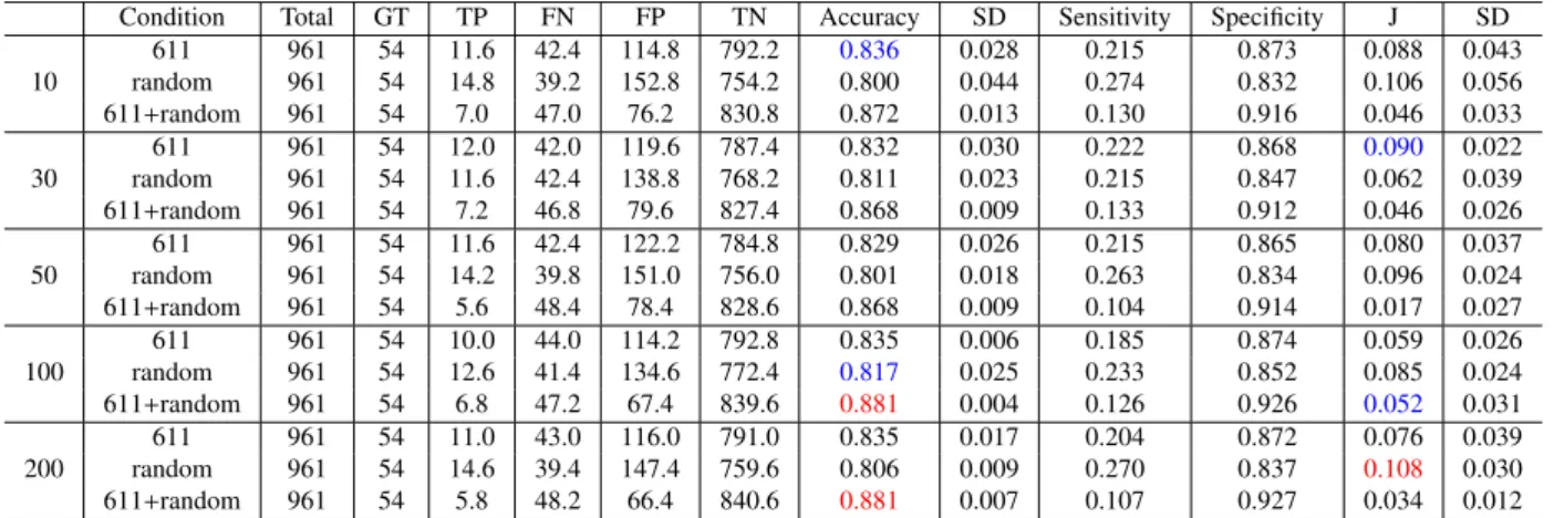
Tables 5 and 6 show results of a prediction for 10 upper wafers when #751 wafer was used as an input. Table 5 cor-responds to occurrence predictions of dislocation clusters in #761 wafer for #751 wafer as an input. Table 6 shows re-sults for dislocation clusters in #761, but it’s not dislocation clusters in #751. We compared them to results of bag of
200 random 961 165 53.8 111.2 108.2 687.8 0.772 0.004 0.326 0.864 0.190 0.018
611+random 961 165 26.6 138.4 45.6 750.4 0.809 0.005 0.161 0.943 0.104 0.018
Table 6 Result of occurrence prediction of 10 upper wafers for #751 wafer input (Dislocation in #761 wafer, not dislocation in #751).
Condition Total GT TP FN FP TN Accuracy SD Sensitivity Specificity J SD
611 961 54 11.6 42.4 114.8 792.2 0.836 0.028 0.215 0.873 0.088 0.043 10 random 961 54 14.8 39.2 152.8 754.2 0.800 0.044 0.274 0.832 0.106 0.056 611+random 961 54 7.0 47.0 76.2 830.8 0.872 0.013 0.130 0.916 0.046 0.033 611 961 54 12.0 42.0 119.6 787.4 0.832 0.030 0.222 0.868 0.090 0.022 30 random 961 54 11.6 42.4 138.8 768.2 0.811 0.023 0.215 0.847 0.062 0.039 611+random 961 54 7.2 46.8 79.6 827.4 0.868 0.009 0.133 0.912 0.046 0.026 611 961 54 11.6 42.4 122.2 784.8 0.829 0.026 0.215 0.865 0.080 0.037 50 random 961 54 14.2 39.8 151.0 756.0 0.801 0.018 0.263 0.834 0.096 0.024 611+random 961 54 5.6 48.4 78.4 828.6 0.868 0.009 0.104 0.914 0.017 0.027 611 961 54 10.0 44.0 114.2 792.8 0.835 0.006 0.185 0.874 0.059 0.026 100 random 961 54 12.6 41.4 134.6 772.4 0.817 0.025 0.233 0.852 0.085 0.024 611+random 961 54 6.8 47.2 67.4 839.6 0.881 0.004 0.126 0.926 0.052 0.031 611 961 54 11.0 43.0 116.0 791.0 0.835 0.017 0.204 0.872 0.076 0.039 200 random 961 54 14.6 39.4 147.4 759.6 0.806 0.009 0.270 0.837 0.108 0.030 611+random 961 54 5.8 48.2 66.4 840.6 0.881 0.007 0.107 0.927 0.034 0.012
Table 7 Result of occurrence prediction of 10 upper wafers for #751 wafer input (Dislocation in #761 wafer) (Bag of features).
Condition Total GT TP FN FP TN Accuracy SD Sensitivity Specificity J SD
611 961 165 42.8 122.2 205.0 591.0 0.660 0.005 0.259 0.742 0.002 0.032
BOF random 961 165 44.6 120.4 221.2 574.8 0.645 0.007 0.270 0.722 -0.008 0.035
611+random 961 165 44.4 120.6 207.0 589.0 0.659 0.013 0.269 0.740 0.009 0.020
Table 8 Result of occurrence prediction of 10 upper wafers for #751 wafer input (Dislocation in #761 wafer, not dislocation in #751) (Bag of features).
Condition Total GT TP FN FP TN Accuracy SD Sensitivity Specificity J SD
611 961 54 11.0 43.0 236.8 670.2 0.709 0.011 0.204 0.739 -0.057 0.042
BOF random 961 54 11.6 42.4 254.2 652.8 0.691 0.007 0.215 0.720 -0.065 0.078
611+random 961 54 13.4 40.6 238.0 669.0 0.710 0.015 0.248 0.738 -0.014 0.037
features (visual words) are shown in Tables 7 and 8. The best values of accuracies are obtained by the 611+random condition. The values are higher than 20 up-per wafers predictions. Results of bag of features are also improved about 0.02 (Table 7) and 0.05 (Table 8). However, amounts of improvement in results of transfer leaning are larger than them, that is, about 0.04 (Table 5) and 0.07 (Ta-ble 6). The sensitivities are low under the conditions that accuracies are high as similar to results of 20 wafers case.
We focused on values of Youden’s J. Maximum val-ues of Youden’s J were obtained under the condition of ran-domly selected negative examples. In any epochs condi-tions, it can be seen a similar tendency, although 20 wafers results are not clear for differences of conditions of negative examples. These values are higher than results of 20 up-per wafers prediction. Amounts of improvement scores are about 0.1 points from values in Table 1 and 0.02 from ones in Table 2. Since results of bag of features are about 0, and
it is worse than results of 20 wafers case. results of transfer learning are better than ones of bag of features.
To compare results in Tables 5 and 6, the best result of J in Table 6 that is the condition of dislocation regions images are exclude is lower than the best value in Table 5. In 10 wafers condition, it shows a tendency that values of J under the condition using randomly selected images as neg-ative examples are larger, as epochs are increased. There-fore, we consider that 10 wafers sampling for a randomly selected way as a negative examples fit for this prediction task. To compare between 611 and 611+ random, we can see that random examples takes a role of increasing both the sensitivity and a specificity. To compare between random and 611+ random, we can see that 611 examples takes a role of decreasing the sensitivity and increasing a specificity. Since 611+ conditions leads increasing the total numbers of negative examples, it is a reasonable specificity is increase. However, 611 examples lead to underperformance.
4. Discussion
We applied transfer learning to occurrence predictions of dislocation clusters in 10 or 20 upper wafers. Both indexes of accuracies and Youden’s J did not reach at 1 for test im-ages (sub-imim-ages of #751 wafer). Accuracies are 0.7 to 0.8, and Youden’s Js are 0.1 to 0.2, approximately, they are low scores. Predictions in 20 upper wafers are worse results than ones in 10 upper wafers. The results in 20 wafers, obvi-ous tendencies are not obtained for differences of negative examples conditions. We conjecture that 20 upper wafers prediction is more difficult task than predictions in 10 upper wafers under this experiment settings. It may mean that 20 wafer sampling is too much for predictions. It may include some of them are not appreciate examples as positive exam-ples. It is difficult for even 10 upper wafers prediction con-dition, when we evaluate the performances by the values of Youden’s J. However, we obtained a tendency in the condi-tion of using randomly selected image as negative examples. Based on the this, we obtained the guide of selections of the negative examples. A randomly selection way is better than an extraction way from one specific wafer. It may show the some image features for each layer have an inherent prop-erty even we can’t see image features by an appearance of an sub-image. It is an interesting point from the view of the physical grains structures composed in a sub-image, if it is embedded the information of a crystalline growth mecha-nism. Humans can’t see it through image features, the net-work can utilize the image features.
As a reason that we examine the results under a condi-tion that a sub-image includes dislocacondi-tion clusters in a pre-diction wafer and does not include dislocation clusters at the same location in input wafer (Tables 2 and 6), we de-sire to predict to occur a new generation point of dislocation clusters. Therefore, we expected to exclude the same dis-location clusters by an above criterion. However, this crite-rion allows to include detections of regions which are caused by a growth up of neighbor dislocation clusters in the input
wafer. Dislocation clusters do not always extend upwards. Slant clusters are often observed. Some values of results in Tables 2 and 6 will include predictions of this case.
5. Conclusion
We examined a prediction method of occurrences of dislo-cation clusters in the upper wafers. We applied a method of a transfer learning of the convolutional neural network to realize a prediction system. As positive examples, im-ages are collected the lower 20 wafers or 10 wafers from the bottom of dislocation clusters. Performances of predic-tions were examined under three condipredic-tions of negative ex-amples, images of some depth wafer (#611), or randomly selected images, or both images. We showed results of ac-curacies and Youden’s J statistic. Performances were not so high, however, these are higher than results by a method of bag of features (visual words). Indexes from sensitivity and specificity show low values, however, we obtained re-sults that randomly select condition as negative examples is better in 10 upper wafers prediction. For 20 upper wafers prediction, the differences of negative examples are not seen as an obvious tendency. It implies that 20 wafers sampling is over to perform the prediction task, and it includes un-appreciate examples as positive examples. From different negative samplings, A randomly selection way is better than an extraction way from one specific wafer. Although sam-pling of one specific wafer leads the underperformance of the network, the system can utilized the image features for each layer have an inherent property even we can’t see im-age features by an appearance of an sub-imim-age.
For further improvement, we are planning to introduce not only pixel intensities of sub-image of a wafer but physi-cal properties of a wafer as input of neural networks. Acknowledgments
This research was supported in part by JST/CREST (JP-MJCR17J1).
References
[1] Y. Hayama, T. Matsumoto, T. Muramatsu,, K. Kutsukake, H. Kudo, and N. Usami, “3D visualization and analysis of dislocation clusters in multicrystalline silicon ingot by approach of data science,” Solar Energy Materials and Solar Cells, vol.189, pp.239–244, 2019. [2] K. Tajima, K. Kutsukake, T. Matsumoto, H. Kudo, and N. Usami,
“The relationship between detection of dislocation clusters in mul-ticrystalline silicon through image processing of macro PL images and carrier recombination,” 79th JSAP Autumn Meeting, 20a-133-2, 2018 (in Japanese).
[3] H. Kudo, Y. Hayama, T. Matsumoto, K. Kutsukake, and N. Usami, “Estimation by non-matrix factorization of dislocation regions in photoluminescence image of multicrystalline silicon,” IEICE Tech-nical Report, 117, 356, pp.13–18, 2017 (in Japanese).
[4] M.N. Schmidt and M. Mørup,“Nonnegative matrix factor 2-D de-convolution for blind single channel source separation,” Proc. 6th international conference on Independent Component Analysis and Blind Signal Separation (ICA’06), pp.700–707, 2006.
of dimensionality of multilayer perceptron estimating dislocation re-gions in multicrystalline silicon photoluminescence image,” IEICE Technical Report, 118, 256, pp.19–24, 2018 (in Japanese). [11] H. Kudo, Y. Hayama, T. Matsumoto, K. Kutsukake, and N. Usami,
“Prediction of regions including dislocations in multicrystalline sili-con photoluminescence image by transfer learning of sili-convolutional neural network,” ICONIP 2019 Proceedings (Australian Journal of Intelligent Information Processing Systems), vol.15, no.2, pp.68–74, 2019.
[12] A. Krizhevsky, I. Sutskever, and G.E. Hinton, “ImageNet classifica-tion with deep convoluclassifica-tional neural networks,” Advances in Neural Information Processing Systems, vol.25, pp.1097–1105, 2012. [13] M.W. Akram, G. Li, Y. Jin, X. Chen, C. Zhu, and A. Ahmad,
“Au-tomatic detection of photovoltaic module defects in infrared images with isolated and develop-model transfer deep learning,” Solar En-ergy, vol.198, pp.175–186, 2020.
[14] W.J. Youden, “Index for rating diagnostic tests,” Cancer, vol.3, no.1, pp.32–35, 1950.
[15] G. Csurka, C.R. Dance, L. Fan, J. Willamowski, and C. Bray, “Vi-sual categorization with bags of keypoints,” Workshop on Statistical Learning in Computer Vision, ECCV, 1, 2004.
[16] H. Kudo, T. Matsumoto, K. Kutsukake, and N. Usami, “Occur-rence prediction of dislocation regions in photoluminescence image of multicrystalline silicon wafers using transfer learning of convolu-tional neural network,” Proc. 10th Internaconvolu-tional Workshop on Image Media Quality and its Applications (IMQA2020), OS3-2-1–OS3-2-5, 2020.
Hiroaki Kudo received the degrees of B. Eng., M. Eng. and D. Eng. at Nagoya Uni-versity, Japan in 1991, 1993 and 1996, respec-tively. In April 1996, he was a faculty member of Nagoya University as a Research Associate. In April 1999, he was an Assistant Professor. Since August 2000, he has been an Associate Professor. Currently, he is a member of Grad-uate School of Informatics, Nagoya University. He was a Research Fellow of the Japan Society for the Promotion of Science in 1995. His re-search interests include visual perception and computer vision.
searcher of Center for Advanced Intelligence Project, RIKEN. He received the degrees of B. Sci., M. Sci. and Dr. Sci from Tohoku Uni-versity in 2002, 2004 and 2007, respectively. From April 2007 to July 2007, he worked as a research fellowship for young scientists (PD) in Japan Society for the Promotion of Science. From August 2007 to March 2010 and from Au-gust 2010 to October 2017, he worked as an as-sistant professor at Institute for Materials Re-search, Tohoku University. From April 2010 to July 2010, he worked as an assistant professor at Graduate School of Energy Science, Kyoto Uni-versity. From November 2017 to July 2018, he worked as a designated lecturer at Institutes of Innovation for Future Society. Since August 2018, he has been with RIKEN. His current research interest is application of data science technique to the research of crystal engineering.
Noritaka Usami is Professor of Gradu-ate School of Engineering at Nagoya University. He received the B.E. and M.E. degrees from the University of Tokyo in 1991 and 1993, re-spectively. From July 1994 to January 2000, he worked as a research associate at Research Cen-ter for Advanced Science and Technology, The University of Tokyo. After recieving his phD in January 1998, he spent 10 months at Instit¨ut f¨ur Angewandte Photophysik, Technische Uni-versit¨at Dresden as a visiting researcher. From February 2000 to March 2013, he worked as an associate professor at In-stitute for Materials Research, Tohoku University. Since 2013, he has been with Nagoya University. His research interest covers crystal growth and characterizations of Si-based materials for photovoltaic and electronic ap-plications, and development of a new methodology for novel materials by fusion of experiments, computation, and data science. He has received var-ious awards, including the best paper award at PVSEC (2009), the best poster award at IEEE PVSC (2012), JSPS Innovative PV Award (2017), and so on.