Japan Advanced Institute of Science and Technology
JAIST Repository
https://dspace.jaist.ac.jp/
Title
Output properties of C_<60> field-effect
transistors with different source/drain
electrodes
Author(s)
Takahashi, Nobuya; Maeda, Akira; Uno, Koichi;
Shikoh, Eiji; Yamamoto, Yoshiyuki; Hori,
Hidenobu; Kubozono, Yoshihiro; Fujiwara, Akihiko
Citation
Applied physics letters, 90(8): 083503-1-083503-3
Issue Date
2007-02
Type
Journal Article
Text version
publisher
URL
http://hdl.handle.net/10119/4020
Rights
Copyright 2007 American Institute of Physics.
This article may be downloaded for personal use
only. Any other use requires prior permission of
the author and the American Institute of Physics.
The following article appeared in Nobuya
Takahashi, Akira Maeda, Koichi Uno, Eiji Shikoh,
Yoshiyuki Yamamoto, and Hidenobu Hori, Applied
Physics Letters 90(8), 083503 (2007) and may be
found at http://link.aip.org/link/?apl/90/083503.
Output properties of C
60field-effect transistors with different source/drain
electrodes
Nobuya Takahashi, Akira Maeda, Koichi Uno, Eiji Shikoh, Yoshiyuki Yamamoto, and Hidenobu Hori
School of Materials Science, Japan Advanced Institute of Science and Technology, Ishikawa 923-1292, Japan
Yoshihiro Kubozono
Department of Chemistry, Okayama University, Okayama 700-8530, Japan Akihiko Fujiwaraa兲
School of Materials Science, Japan Advanced Institute of Science and Technology, Ishikawa 923-1292, Japan
共Received 24 November 2006; accepted 23 January 2007; published online 21 February 2007兲 C60 field-effect transistors 共FETs兲 have been fabricated with source/drain electrodes of three
different materials, indium tin oxide共ITO兲, Au, and Pt. High field-effect mobilityFEof FETs with
ITO electrodes, 1.6⫻10−1cm2/ V s, shows that ITO is a potential material for the electrodes of
organic electronics. Although the highest Schottky barrier and the lowestFEwere expected,FE
of FET with Pt electrodes 共1.4⫻10−1cm2/ V s兲 is higher than that of FET with Au electrodes
共9.6⫻10−2cm2/ V s兲. The result suggests that modification of local electronic structure at the
interface between electrodes and C60 affects device performance. © 2007 American Institute of Physics. 关DOI:10.1063/1.2709523兴
Organic field-effect transistors 共OFETs兲 have great po-tential for next-generation electronic devices because of their inexpensive price, light weight, mechanical flexibility, and high-shock resistance.1Performance of OFETs has been dra-matically improved, and the mobility has become compa-rable to that of amorphous Si共a-Si兲 during recent years.2–5 From the systematic and detailed characterization of OFETs,6–11 it has been clarified that the device performance of OFETs strongly depends on parasitic resistance at the in-terface between the source/drain electrodes 共an inorganic metal兲 and the channel 共an organic semiconductor兲. Domi-nant origin of the parasitic resistance was thought to be the Schottky barrier at the interface between electrodes and the channel. Simply, the barrier height is estimated by Mott-Schottky relationship, namely, the energy difference between the Fermi energy共EF兲 of an electrode and the energy level of the lowest unoccupied molecular orbital共LUMO兲 ELUMOof
an organic semiconductor for electrons, and that between EF of an electrode and the energy level of the highest occupied molecular orbital 共HOMO兲 EHOMO of an organic
semicon-ductor for holes. Actually, by reducing the energy difference between the EFand ELUMO共EHOMO兲, the device performance
of n-type 共p-type兲 FETs including field-effect mobilityFE
was improved.9,10,12–14
Local electronic structure at the interface between an inorganic metal and an organic material has also been vigor-ously investigated.15 Experimental16,17 and theoretical18,19 studies showed that charge transfer between metals and mol-ecules occurs, and the valence of molmol-ecules at the interface is not neutral. Appearance of dipole moment at interface in-duced by a charge transfer was also proposed.20 From these studies, it was clarified that the carrier injection barrier can
be attributed not only to the Mott-Schottky relationship but also to the effects of vacuum-level shift and local electric dipole due to the charge transfer and hybridization between an inorganic metal and an organic material. The fact that the carrier injection barrier depends on the molecular orientation near source/drain electrodes provides evidence of these ad-ditional effects.21
For the application of OFETs to electronic devices, such as complementary metal-oxide semiconductors共CMOS兲, de-tailed characterization of contact resistance and development of electrodes available to both p- and n-type OFETs are re-quired. Indium tin oxide共ITO兲 is well known as a transpar-ent anode for organic light emitting diodes. Furthermore, it is also expected to be used for source/drain electrodes of n-type OFETs, because work function of ITO is smaller than those of typical electrode materials of n-type OFETs such as Au. In the present study, we have fabricated C60 FETs
with source/drain electrodes of three different materials, ITO 共In2O3+ SnO2 10 wt %兲, Au, and Pt, and have investigated
their output properties.
C60FETs were fabricated with a bottom contact
configu-ration, as shown in Fig.1共a兲. A heavily doped n-type silicon wafer with 400 nm thickness of thermally oxidized SiO2
layer on the surface was used as substrate. The source and drain electrodes were patterned on insulating SiO2layer,
us-ing a photolithography method: the channel length L and the channel width W were designed to be 10 and 500m, re-spectively. For the devices with electrodes of ITO, a film was deposited using rf magnetron sputtering共Tokuda CFS-4ES兲 at a nominal deposition rate of 0.4 nm/ s under argon flow at the pressure of 0.50 Pa. For the devices with electrodes of Au or Pt, films of Au and Pt were deposited using dc sput-tering共Elionix ECS101兲 at deposition rates of about 0.06 and 0.08 nm/ s, respectively. The thickness of source/drain elec-trodes was fixed to be 100 nm independent of the electrode materials. The doped silicon layer of the wafer was used as a
a兲Author to whom correspondence should be addressed; electronic mail: [email protected]
APPLIED PHYSICS LETTERS 90, 083503共2007兲
0003-6951/2007/90共8兲/083503/3/$23.00 90, 083503-1 © 2007 American Institute of Physics
gate electrode. Commercially available C60 共99.98%兲 was used for the formation of the thin film channel layer. A C60
thin film of 150 nm thickness was formed using vacuum 共⬍10−5Pa兲 vapor deposition at the deposition rate of
0.1 nm/ s. FETs fabricated by this procedure were exposed to air during the transfer from the deposition chamber to a mea-surement chamber. Before meamea-surements, therefore, the samples were annealed at 120 ° C under 10−3Pa for 24 h in order to remove adsorbed O2 and/or H2O molecules.
Trans-port properties of C60FETs were measured at room tempera-ture under 10−3Pa without exposure to air after annealing
using prober system共Desert TT-prober, Keithley 4200-SCS兲. In this study, in order to reduce the influence of the small number of adsorbed O2 and/or H2O molecules, all
fabrica-tion and experimental processes of three types of devices except for the deposition of source/drain electrodes was per-formed under the same condition. In addition, more than three series of these experiments were repeated, and data were compared within the same series. For the estimation of of ITO, Au, and Pt, the films of these materials fabricated by the same procedure were investigated by photoemission 共PE兲 spectroscopy 共Riken Keiki AC-2兲.
Figures 1共b兲–1共d兲 show the output characteristics, namely, the drain current IDversus the drain-source voltage VDS plots, for C60 FET with source/drain electrodes of ITO, Au, and Pt. IDincreases almost linearly with increasing VDS,
followed by saturation due to the pinchoff of the accumula-tion layer; all FETs in this work show typical n-type
nor-mally off characteristics. Hysteresis of ID’s with VDS sweep was very small. The plots of ID1/2versus the gate voltage VG
for all devices at VDS= 80 V are shown in Fig. 2. TheFE
and threshold voltage VTwere determined from the relation,
ID=共FEWC0/ 2L兲共VG-VT兲2, at saturation regime.FEand VT were 1.6⫻10−1 cm2/ V s and 36 V for the device with ITO
source/drain electrodes, 9.6⫻10−2 cm2/ V s and 42 V for
that with Au electrodes, and 1.4⫻10−1cm2/ V s and 41 V
for that with Pt electrodes, respectively. Here, we use 1.0 ⫻10−8F / cm2 as the capacitance per area of gate insulator
SiO2共C0兲 estimated from dielectric constant and thickness of
SiO2, because this estimation is consistent with experimental
results.22 The current on-off ratios, ID共VG= 80 V兲/ID共VG
= 0 V兲, are 4.0⫻106 共ITO兲, 2.5⫻106 共Au兲, and 3.3⫻106
共Pt兲. Derived device parameters for all devices are summa-rized in TableI.
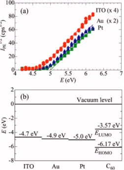
PE spectra of the films of ITO, Au, and Pt are shown in Fig.3共a兲. The square root of intensity IPE1/2was proportional to energy of incident light E for all samples.was determined as threshold energy ET from the relation, IPE
1/2= a共E−E
T兲+b, where a is just a fitting parameter, and b is background. Values of estimatedare summarized in TableI, and in Fig.
3共b兲 with energy diagram. They are consistent with those in the literature.23–25 ELUMO and EHOMO of C60 are taken from
Refs. 26 and 27 as 3.57 and 6.17 eV, respectively. From these values, the expected Schottky barrier heights at the interface between electrodes共ITO, Au, and Pt兲 and the chan-nel 共C60兲 are 1.13, 1.33, 1.43 eV, respectively. It was re-ported that the device performance of C60 FETs is affected by large contact resistance between electrodes and the chan-nel of C60,11 which results in lower values of FE.10 FETs
with lower carrier injection barriers show higher values of FE. Consistent with this analogy, FE of a FET with ITO
FIG. 2.共Color online兲 ID1/2vs V
Gplots at VDS= 80 V for all C60FET devices. Solid lines are the fitting results of data for VG⬎60 V, using the equation in the text.
FIG. 1.共Color online兲 共a兲 Device structure of C60 thin-film FET. IDvs VDSplots for C60FET with source/drain electrodes of共b兲 ITO, 共c兲 Au, 共d兲 Pt. Gate voltages were applied from 0 to 80 V.
TABLE I. Device characteristics and work functionof source/drain elec-trodes for all devices.
Source/drain electrodes ITO Au Pt 共cm2/ V s兲 1.6⫻10−1 9.6⫻10−2 1.4⫻10−1
VT共V兲 36 42 41
On-of ratio 4.0⫻106 2.5⫻106 3.3⫻106
共eV兲 4.7 4.9 5.0
083503-2 Takahashi et al. Appl. Phys. Lett. 90, 083503共2007兲
electrodes is the highest among the three types of FETs in this study. The result shows that ITO, which is one of the typical hole-injection electrodes for p-type organic semicon-ductors, can also be a good electron-injection electrode for
n-type organic semiconductors such as C60. In addition, ITO
provides very stable electrodes with small, whereas metal electrodes with smallare very sensitive to air and should be used in vacuum.9,10This implies that the use of ITO as an electrode is very effective for transparent organic electronic devices containing both p- and n-type FETs, such as CMOS. FE of the FET with Pt electrodes, which was expected
to be the lowest among FETs in this work, is higher than that of FET with Au electrodes and is very close to that of FET with ITO electrodes. We repeated the same series of experi-ments more than three times. In these experiexperi-ments, the trend was invariant, although absolute values of device parameters varied slightly in each series. The origin of this discrepancy from Mott-Schottky limit may be attributed to modification of local electronic structure at the interface between elec-trodes and C60due to charge transfer and/or hybridization of
orbitals such as -d interaction.16–20 Our results show that device performance of organic FETs can be greatly improved by precisely controlling the electronic structure at the inter-face between electrodes and active layer of organic semicon-ductors.
In conclusion, we have succeeded to fabricate C60FETs
with source/drain electrodes of three different materials, ITO, Au, and Pt. The highestFEvalue of 1.6⫻10−1 cm2/ V s in
this work has been obtained in the C60FETs with ITO
elec-trodes, showing that ITO can be used not only for the hole-injection electrodes for p-type organic semiconductors but also for the electron-injection electrodes for n-type organic semiconductors such as C60. This implies that the use of ITO
as an electrode will contribute to development of transparent
organic electronics.FEof the FET with Pt electrodes, which
was expected to be the lowest among FETs in this work, is higher than that of FET with Au electrodes. The result sug-gests the modification of local electronic structure at the in-terface between electrodes and a channel of C60 due to charge transfer and/or hybridization of orbitals.
The authors are grateful to the staff of the Center for Nano Materials and Technology at the Japan Advanced Insti-tute of Science and Technology for technical support. This work is supported in part by the Grant-in-Aid for Scientific Research共Grant Nos. 16206001, 17310059, 17540322兲 from the Ministry of Education, Culture, Sports, Science and Technology 共MEXT兲 of Japan, a NEDO grant 共Grant No. 04IT5兲 from the New Energy and Industrial Technology De-velopment Organization共NEDO兲, and a Grant from Kurata Memorial Hitachi Science and Technology Foundation.
1C. D. Dimitrakopoulos and D. J. Mascaro, IBM J. Res. Dev. 45, 11 共2001兲.
2V. Podzorov, S. E. Sysoev, E. Loginova, V. M. Pudalov, and M. E. Gershenson, Appl. Phys. Lett. 83, 3504共2003兲.
3P. R. L. Malenfant, C. D. Dimitrakopoulous, J. D. Gelorme, L. L. Kosbar, and T. O. Graham, Appl. Phys. Lett. 80, 2517共2002兲.
4S. Kobayashi, T. Takenobu, S. Mori, A. Fujiwara, and Y. Iwasa, Appl. Phys. Lett. 82, 4581共2003兲.
5K. Itaka, M. Yamashiro, J. Yamaguchi, M. Haemori, S. Yaginuma, Y. Matsumoto, M. Kondo, and H. Koinuma, Adv. Mater.共Weinheim, Ger.兲
18, 1713共2006兲.
6I. Yagi, K. Tsukagoshi, and Y. Aoyagi, Appl. Phys. Lett. 84, 813共2004兲. 7B. H. Hamadani and D. Natelson, J. Appl. Phys. 95, 1227共2004兲. 8P. V. Pesavento, R. J. Chesterfield, C. R. Newman, and C. D. Frisbie, J.
Appl. Phys. 96, 7312共2004兲.
9T. Ohta, T. Nagano, K. Ochi, Y. Kubozono, E. Shikoh, and A. Fujiwara, Appl. Phys. Lett. 89, 053508共2006兲.
10K. Ochi, T. Nagano, T. Ohta, R. Nouchi, Y. Kubozono, Y. Matsuoka, E. Shikoh, and A. Fujiwara, Appl. Phys. Lett. 89, 083511共2006兲. 11Y. Matsuoka, K. Uno, N. Takahashi, A. Maeda, N. Inami, E. Shikoh, Y.
Yamamoto, H. Hori, and A. Fujiwara, Appl. Phys. Lett. 89, 173510 共2006兲.
12T. Takahashi, T. Takenobu, J. Tkeya, and Y. Iwasa, Appl. Phys. Lett. 88, 033505共2006兲.
13Y. Takahashi, T. Hasegawa, Y. Abe, Y. Tokura, and G. Saito, Appl. Phys. Lett. 88, 073504共2006兲.
14T. Maeda, H. Kato, and H. Kawakami, Appl. Phys. Lett. 89, 123508 共2006兲.
15For an overview, see H. Ishii, N. Hayashi, E. Ito, Y. Washizu, K. Sugi, Y. Kimura, M. Niwano, O. Ouchi, and K. Seki, in Physics of Organic
Semi-conductors, edited by W. Brütting共Wiley-VCH, Berlin, 2005兲, Chap. 3,
69–94.
16B. W. Hoogenboom, R. Hesper, L. H. Tjeng, and G. A. Sawatzky, Phys. Rev. B 57, 11939共1998兲.
17R. Nouchi and I. Kanno, J. Appl. Phys. 97, 103716共2005兲. 18L.-L. Wang and H.-P. Cheng, Phys. Rev. B 69, 045404共2004兲. 19L.-L. Wang and H.-P. Cheng, Phys. Rev. B 69, 165417共2004兲. 20S. C. Veenstra, A. Heeres, G. Hadziioannou, G. A. Sawatzky, and H. T.
Jonkman, Appl. Phys. A: Mater. Sci. Process. 75, 661共2002兲.
21K. Ihm, B. Kim, T.-H. Kang, K.-J. Kim, M. H. Joo, T. H. Kim, S. S. Yoon, and S. Chung, Appl. Phys. Lett. 89, 033504共2006兲.
22K. Shibata, Y. Kubozono, T. Kanbara, T. Hosokawa, A. Fujiwara, Y. Ito, and H. Shinohara, Appl. Phys. Lett. 84, 2572共2004兲.
23H. B. Michaelson, J. Appl. Phys. 48, 4729共1977兲. 24I. D. Parker, J. Appl. Phys. 75, 1656共1994兲.
25Y. Park, V. Choong, Y. Gao, B. R. Hsieh, and C. W. Tang, Appl. Phys. Lett. 68, 2699共1996兲.
26N. Sato, Y. Saito, and H. Shinohara, Chem. Phys. 162, 433共1992兲. 27N. Hayashi, H. Ishii, Y. Ouchi, and K. Seki, J. Appl. Phys. 92, 3784
共2002兲. FIG. 3.共Color online兲 共a兲 PE spectra of the films of ITO, Au, and Pt. Solid
lines are the fitting results of data, using the equation in the text.共b兲 Energy diagram of ITO, Au, Pt, and C60. Work functionof ITO, Au, and Pt are experimental data estimated from PE spectra. ELUMOand EHOMOof C60are taken from Refs.26and27.
083503-3 Takahashi et al. Appl. Phys. Lett. 90, 083503共2007兲