Japan Advanced Institute of Science and Technology
JAIST Repository
https://dspace.jaist.ac.jp/Title
Scanning tunneling microscopy of Dy@C_<82> and
Dy@C_<60> adsorbed on Si(111)-(7×7) surfaces
Author(s)
Fujiki, S; Kubozono, Y; Hosokawa, T; Kanbara, T;
Fujiwara, A; Nonogaki, Y; Urisu, T
Citation
Physical Review B, 69(4): 045415-1-045415-5
Issue Date
2004-01
Type
Journal Article
Text version
publisher
URL
http://hdl.handle.net/10119/3366
Rights
Satoshi Fujiki, Yoshihiro Kubozono, Tomoko
Hosokawa, Takayoshi Kanbara, Akihiko Fujiwara,
Youichi Nonogaki and Tsuneo Urisu, Physical
Review B, 69(4), 045415, 2004. "Copyright 2004 by
the American Physical Society."
http://scitation.aip.org/getabs/servlet/GetabsSer
vlet?prog=normal&id=PRBMDO00006900000404541500000
1&idtype=cvips&gifs=yes
Scanning tunneling microscopy of Dy@C
82and Dy@C
60adsorbed on Si
„111…-„7Ã7… surfaces
Satoshi Fujiki,1,2 Yoshihiro Kubozono,2,3,* Tomoko Hosokawa,2,3 Takayoshi Kanbara,4 Akihiko Fujiwara,2,5Youichi Nonogaki,6,7and Tsuneo Urisu1,6
1Department of Structural Molecular Science, Graduate University for Advanced Studies, Okazaki 444-8585, Japan 2CREST, Japan Science and Techonology Corporation, Kawaguchi 332-0012, Japan
3Department of Chemistry, Okayama University, Okayama 700-8530, Japan 4Institute for Material Research, Tohoku University, Sendai 980-8577, Japan 5Japan Advanced Institute of Science and Technology, Ishikawa 923-1292, Japan
6Department of Vacuum UV Photoscience, Institute for Molecular Science, Okazaki 444-8585, Japan 7Department of Functional Molecular Science, Graduate University for Advanced Studies, Okazaki 444-8585, Japan
共Received 29 July 2003; published 28 January 2004兲
Dy@C82and Dy@C60adsorbed on Si(111)-(7⫻7) surface are investigated by scanning tunneling
micros-copy共STM兲 at 295 K. The Dy@C82molecules in the first layer are adsorbed on the Si(111)-(7⫻7) surface without formation of islands and nucleation, and the internal structure of the Dy@C82 molecule is first
observed on the surface at 295 K. The average heights of the Dy@C82molecules in the first and second layers
are estimated to be 7.2 and 10.8 Å, respectively, by STM. These results suggest strong interactions between the Si atoms and the Dy@C82molecules in the first layer. The STM image reveals that the Dy@C60molecule is
nearly spherical, showing that the metal endohedral C60possesses a cage-form structure.
DOI: 10.1103/PhysRevB.69.045415 PACS number共s兲: 68.43.Fg, 68.37.Ef, 81.07.⫺b
I. INTRODUCTION
Metallofullerene molecules have attracted special atten-tion from physicists and chemists owing to their unique structures.1Furthermore, the metallofullerenes have been no-table as research subjects in nanometer-scale science because the molecular size is⬃1 nm and unique electronic structures are expected at molecular and cluster levels. Scanning tun-neling microscopy共STM兲 is a powerful technique for study-ing the structures and electronic properties of metallof-ullerenes at the nanometer scale. Recently, the adsorption characteristics of metallofullerenes on semiconductor sur-faces have been studied extensively by STM.2– 6
A STM image of Sc2@C84 adsorbed on Si(100)-(2⫻1)
surface was first reported by Shinohara et al. and showed a nearly spherical structure of the Sc2@C84 molecule.2 The
first layer of Sc2@C84 was not ordered, owing to strong
in-teractions between the surface and the molecules. Further, the Sc2@C84molecules in the first layer possessed no pref-erential adsorption positions such as terrace edges and defect sites on the Si(100)-(2⫻1) surface, and showed no specific nucleation. The third layer of Sc2@C84 on the Si(100)-(2
⫻1) surface was ordered to form a hexagonally close-packed array, and the nearest-neighbor distance d between the molecules was 11.7 Å, which is slightly smaller than that 共12.1 Å兲 in a close-packed C84 array.7 This implies that the
third layer is dominated by van der Waals interactions be-tween the Sc2@C84 molecules.
The structure and electronic properties of Dy@C82 have
been studied by x-ray powder diffraction, x-ray absorption near edge spectroscopy 共XANES兲, and electric resistivity measurements.8 –10 The x-ray diffraction pattern for mixed crystals of Dy@C82isomers I and II at 298 K was indexed in a face-centered cubic共fcc兲 structure with a lattice constant a of 15.86共1兲 Å. XANES of a crystalline Dy@C82 sample
showed that the valence of Dy was ⫹3. The temperature dependence offor a Dy@C82thin film showed a
semicon-ductorlike behavior with the gap energy Eg of 0.2 eV. Studies of M @C60( M : metal atoms兲 have scarcely been
carried out because of difficulties in obtaining macroscopic amounts of purified samples, although the structures and the expected physical properties such as molecular metals and superconductivity have attracted much interest from physi-cists and chemists. Recently, Dy@C60 was extracted with
aniline and purified by high-performance liquid chromatography.11 XANES of Dy@C60 revealed a valence
of ⫹3 for the Dy atom. The center frequency 0 of the
Ag(2) Raman peak for Dy@C60was 1450 cm⫺1, also show-ing that the valence of Dy was ⫹3. More recently, the elec-tronic properties of La@C60 and Ce@C60 adsorbed on highly oriented pyrolytic graphite 共HOPG兲 were studied by STM and scanning tunneling spectroscopy 共STS兲.4 An en-ergy gap Eg of⬃0.3 eV was observed for Ce@C60 by STS
at room temperature, while a zero band gap was observed at room temperature for La@C60, and the gap opened below
28 K.4 In the present study, STM images of Dy@C82 and Dy@C60 molecules adsorbed on Si(111)-(7⫻7) surfaces
are studied at 295 K, in order to clarify the structures and electronic properties at the nanometer scale. The adsorption patterns are observed from the STM images. The structures and electronic properties at the nanometer scale found by STM are compared with those found in the solid and in thin films.
II. EXPERIMENT
Sample preparation and purification of Dy@C82 and
Dy@C60 are described elsewhere.8,11 The Dy@C82 sample
used in the present study contained two isomers I and II with a molar ratio of 4:1. The Si共111兲 substrate was degassed by heating it at 600 °C for 12 h and flash annealing up to
1100 °C for 10 s several times. Furthermore, this substrate was maintained at 700 °C for 3 min and then cooled slowly down to room temperature. The vacuum level was kept be-low 2⫻10⫺9 Torr during these procedures to obtain a well-defined Si(111)-(7⫻7) surface. Powder samples of metal-lofullerenes were deposited on the well-defined Si(111)-(7 ⫻7) surface at 650 °C after annealing the samples at 300 °C for 12 h under⬃1⫻10⫺9 Torr. The deposition rate was kept below 0.1 monolayers 共ML兲/h, and the substrate was not heated during the thermal deposition. All STM measure-ments were performed by using an ultrahigh-vacuum STM system 共UNISOKU Scientific Instruments兲 with Pt-Ir tips. The STM image was measured in the constant-current mode under ⬃5⫻10⫺11Torr. The heights estimated from STM were calibrated with the exact height, 3.1 Å, of the step in the Si substrate. The sample bias voltage Vs and tunneling
current Itwere ⫺2.6 to ⫺2.0 V and 0.20–0.25 nA, respec-tively.
III. RESULTS AND DISCUSSION
A typical STM image of Dy@C82molecules adsorbed on
Si(111)-(7⫻7) at 295 K is shown in Fig. 1共a兲; the Dy@C82 molecule surface coverage is 0.1 ML. The bright spherical spots are the images of the Dy@C82molecules. The
mono-mers of the Dy@C82 molecules are adsorbed on the
Si(111)-(7⫻7) surface without formation of islands and nucleation, as in the case of C60 molecules on Si(111)-(7
⫻7) and Sc2@C84 molecules on Si(100)-(2⫻1).3,12 The
adsorption characteristics are different from those of Lu@C82on a C60film, in which an accumulation of Lu@C82
molecules is observed near the step edge.5 The Dy@C82
molecules neither migrate toward the step edge nor make significant clusters even after the substrate was heated up to 200 °C; the STM image was measured at 295 K after anneal-ing. These results imply that Dy@C82molecules are strongly bound by the Si surface.
Three possible adsorption sites for Dy@C82 on the
sur-face are shown in Fig. 1共b兲. 72% of the Dy@C82 molecules
are adsorbed on the A site surrounded by three Si adatoms, and 9% and 19% of the molecules are adsorbed on the corner holes共site B) and on the dimer lines 共site C), respectively. Previously, it was shown that 80% of C60 molecules were
adsorbed on the A site.12 This value is consistent with that found for the Dy@C82molecules, implying that the A site is
very attractive for fullerene molecules. In the case of C60,
13% and 7% of the molecules were adsorbed on the B and C sites, respectively.12 Contrary to the case of Dy@C82, the adsorption probability on the corner holes was larger than that on the dimer lines.12This result may originate from the facts that the van der Waals diameter of the C60 molecule is smaller than that of the Dy@C82molecule and that the
spac-ing of the corner holes (B site兲 is larger than that of the dimer lines (C site兲. The C60molecules can fall in the corner
hole (B site兲 more deeply than the Dy@C82molecules, as is
seen from Fig. 1共c兲, but the spacing of the dimer lines is too small to let the C60 molecule fall deeply into the site; the
details of spacing of each site are described later. The deep
falling of the C60molecule in the corner hole should stabilize
adsorption on the site.
It is predicted by taking into consideration only the van der Waals diameters of the Dy@C82 molecule共11.4 Å兲 and
Si atom共4.2 Å兲 that STM will give heights of 10.0 and 7.7 Å
FIG. 1. 共a兲 STM image for 0.1 ML of Dy@C82adsorbed on the Si(111)-(7⫻7) surface (100⫻100 nm2). Vsand Itwere⫺2.0 V
and 0.20 nA, respectively.共b兲 Schematic diagram of three possible adsorption sites on the Si(111)-(7⫻7) surface. 共c兲 Schematic rep-resentation of Dy@C82and C60molecules captured into the basins
of the Si surface. The van der Waals diameters of Dy@C82and C60
molecules are shown by large gray circles and open circles, respec-tively, in 共c兲. The small gray circles refer to the Si adatoms in 共b兲 and共c兲, and the small open circles and the dots refer to the Si atoms except for the adatoms in共b兲 and 共c兲.
FUJIKI et al. PHYSICAL REVIEW B 69, 045415 共2004兲
for Dy@C82 molecules on the A and B sites, respectively.
This feature is schematically represented in Fig. 1共c兲. These results reflect the facts that the spacing between the Si ada-toms is 7.7 Å in one triangular subunit surrounded by three adatoms (A site兲, and the spacing between the Si adatoms across the corner holes (B site兲 is 13.3 Å; these values are shown in Fig. 1共b兲. The heights of the Dy@C82molecules on the A and B sites are experimentally estimated to be 7.3 and 6.6 Å, respectively, from the STM image. These experimen-tal heights are smaller than the predicted ones, 10.0 and 7.7 Å. Furthermore, the experimental height is estimated to be 7.1 Å for the C site, a value also smaller than the predicted one, 8.5 Å; the spacing of the adatoms across the boundary of the triangle (C site兲 is 6.7 Å. The average height of the Dy@C82molecules observed in the first layer is 7.2 Å. The
heights of the Dy@C82 molecules cannot be explained only
by the fact that the molecules enter basins of the Si surface such as the A, B, and C sites. This implies that the spaces are not large enough to allow the molecules to fall into the basins to reproduce the heights estimated experimentally from the STM. Consequently, we conclude that heights lower than the predicted ones at all sites are realized because of a strong interaction between the Si surface and the Dy@C82
molecules, i.e., formation of a Si-C bond.
The schematic representation 关Fig. 1共c兲兴 shows clearly that the experimental height of 6.6 Å for the Dy@C82
mol-ecule on the B site, lower than those on the A and C sites, 7.3 and 7.1 Å, originates from the fact that the molecule can enter the basin of the B site more deeply than the other sites. At the B site, the difference between the experimental height 共6.6 Å兲 and the predicted one 共7.7 Å兲 is ⫺1.1 Å in Dy@C82.
The difference is the same as that for C60, in which the
experimental and predicted heights are 5.0 and 6.1 Å, respectively.13 This fact implies that the nature of the inter-action between the molecules and Si adatoms at the B site is the same for Dy@C82 and C60. At the A site, the difference between the experimental height 共7.3 Å兲 and the predicted one共10.0 Å兲 is ⫺2.7 Å in Dy@C82, and close to⫺2.9 Å in
C60, in which the experimental and predicted heights are 6.0
and 8.9 Å, respectively.13This result suggests that the inter-action is almost the same for Dy@C82and C60at the A site.
Here we note that the Si-C interaction is much stronger at the A site than the B site because the difference is larger by 2.5 times at the A site than at the B site. This result shows that the A site is very attractive for fullerene molecules, and it rationalizes the fact that more than 70% of the Dy@C82
mol-ecules and C60 molecules are adsorbed on the A site.
High-resolution STM images of the Dy@C82 molecules
observed at 295 K are shown in Fig. 2. Further, the STM images of three Dy@C82 molecules named a, b, and c are
enlarged in the figure. Patterns that reflect the charge distri-bution of the C82 cage are clearly observed in these images;
this kind of pattern is termed the internal structure of the C82
cage. These clear images of the internal structure suggest that the motion of the Dy@C82 molecules is frozen on the
Si(111)-(7⫻7) surface even at 295 K. A correlation be-tween the internal structures and the adsorption sites is not clearly seen in Fig. 2, i.e., the high-resolution STM images
show that the Dy@C82molecules are randomly oriented on
the Si(111)-(7⫻7) surface. Clear spots ascribable to the Dy atoms inside the cages are not observed for any Dy@C82
molecules. This result may originate from a dynamical dis-order of the Dy atom inside the C82cage, as suggested from
a Rietveld analysis for x-ray powder diffraction.10
High-resolution STM images showing the internal struc-ture of metallofullerenes have hardly been reported, although internal structures have been observed for C60 molecules on
the Si(111)-(7⫻7) surface at room temperature.13 The in-ternal structure was not observed in a multilayer film of La@C82 on the Si(111)-(7⫻7) surface.6 In the present
study, the internal structure of the C82 cage has been ob-served owing to the strong interaction between the Si atom and the Dy@C82 molecule in the first layer. More recently,
Shinohara et al. observed the internal structure of La2@C80
and La@C82 in the first layer of a hydrogen-terminated
Si(100)-(2⫻1) surface at 78 K by STM.14
Simulation of the STM image based on a theoretical cal-culation of electronic structure is necessary to determine the internal structure at the atomic level, because the STM image directly reflects the electronic structure of the molecules near the Fermi level. High-resolution STM images make it pos-sible to identify the molecular orientations of metallof-ullerenes on the Si surface, when the atomic level structures are determined by analyses of the STM images. The infor-mation about molecular orientation helps to clarify the
FIG. 2. High-resolution STM image for 0.05 ML of Dy@C82
adsorbed on the Si(111)-(7⫻7) surface (30⫻30 nm2). Vsand It
mechanism for the accumulation of metallofullerenes on the surface. The determination of molecular orientations for vari-ous types of metallofullerenes on a semiconductor surface is now in progress, based on the theoretical simulations for their STM images.
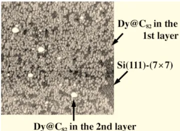
The STM image of the Si(111)-(7⫻7) surface covered with⬃1 ML of Dy@C82 at 295 K is shown in Fig. 3. The
dark regions are the bare surface of Si(111)-(7⫻7). The gray blobs on the Si surface can be ascribed to the Dy@C82
molecules in the first layer, and the bright near-circular fea-tures can be ascribed to the Dy@C82molecules in the second layer. The STM image shows no specific nucleation in the first layer. The first layer is not ordered, as is seen from Fig. 3, and no second layer islands are observed before comple-tion of the first layer. These results indicate that the interac-tion between the Si atoms and the Dy@C82molecules in the
first layer is stronger than the intermolecular interaction be-tween the Dy@C82 molecules. The height of the Dy@C82 molecule共bright ball兲 in the second layer is estimated to be 10.8 Å from the STM image. This value is close to the van der Waals diameter of the Dy@C82molecule, 11.2–11.4 Å.8
This implies that the electronic structure of the Dy@C82
molecules in the second layer is not substantially affected by the Si surface.
The STM image of ⬃0.01 ML Dy@C60 molecules
ad-sorbed on the Si(111)-(7⫻7) surface observed at 295 K is shown in Fig. 4共a兲. The nearly spherical features can be as-cribed to the Dy@C60molecules. This image is similar to a
bright spherical feature for La@C60 on a HOPG reported
previously.4 It was reported that neither La@C60 nor
Ce@C60 molecules formed an island on the HOPG at room
temperature.4The Dy@C60 molecules are also adsorbed on
the surface without islands and do not migrate at 295 K. No spots ascribable to the Dy atoms are observed around the nearly spherical image. A close-up of the image of the Dy@C60molecule is shown in Fig. 4共b兲, which also exhibits
a nearly spherical image. The destruction of the C60 cage is
not found in this image, i.e., the Dy@C60molecule exhibits
a cage-form structure, as suggested from Raman and
ex-tended x-ray absorption fine structure analyses.11The height of the Dy@C60 molecule is estimated to be ⬃7 Å, a value suggesting a strong interaction between the Si atoms and the Dy@C60molecules, as in the Dy@C82molecule. In the STM
image of the Dy@C60 molecules, the spot of the Dy atom
could not clearly be observed inside the cage as in the Dy@C82molecules. Internal structures of the C60cage were
not observed in this image.
IV. CONCLUSION
The adsorption of Dy@C82 and Dy@C60 on the
Si(111)-(7⫻7) surface has been studied by STM at 295 K. In the first layer of Dy@C82 molecules, the molecules are strongly bound by the Si surface, and the internal structures of the C82cage are clearly observed. The internal structure of
the Dy@C82 molecule is first observed at room temperature
owing to the freezing of its dynamical motion through the formation of chemical bonds between the molecule and the Si adatoms on the Si(111)-(7⫻7) surface. The driving force for the arrangement of Dy@C82 in the second layer is van
der Waals interaction. The STM image of the Dy@C60 mol-ecule shows a nearly spherical spot. This is direct and im-portant evidence of a cage-form structure because the struc-ture of metal endohedral C60 has not yet been established.
Information on the structures of Dy@C82and Dy@C60
mol-ecules on a semiconductor surface will open doors to build up nanoscale molecular assemblies with high functionality as well as clarifying directly the nature of individual molecules.
FIG. 3. STM image for ⬃1 ML of Dy@C82 adsorbed on the Si(111)-(7⫻7) surface (80⫻80 nm2). V
sand Itwere⫺2.6 V and
0.25 nA, respectively.
FIG. 4.共a兲 STM images for ⬃0.01 ML of Dy@C60adsorbed on the Si(111)-(7⫻7) surface (40⫻20 nm2). Vsand Itwere⫺2.0 V
and 0.20 nA, respectively. 共b兲 Close-up of a STM image of Dy@C60molecule (10⫻5 nm2).
FUJIKI et al. PHYSICAL REVIEW B 69, 045415 共2004兲
ACKNOWLEDGMENTS
This work was supported by CREST of Japan Science and Technology Corporation, by a Grant-in-Aid 共No. 15350089兲
from the Ministry of Education, Science, Sports and Culture of Japan, and by the Special Research Project and Joint Stud-ies Program of Institute for Molecular Science. S.F. thanks JSPS for financial support.
*Electronic address: [email protected]
1H. Shinohara, Rep. Prog. Phys. 63, 843共2000兲.
2H. Shinohara, N. Hayashi, H. Sato, Y. Saito, X.-D. Wang, T.
Hashizume, and T. Sakurai, J. Phys. Chem. 97, 13 438共1993兲.
3
X.-D. Wang, Q. K. Xue, T. Hashizume, H. Shinohara, Y. Nishina, and T. Sakurai, Phys. Rev. B 48, 15 492共1993兲.
4R. Klingeler, G. Kann, I. Wirth, S. Eisebitt, P. S. Bechthold, M.
Neeb, and W. Eberhardt, J. Chem. Phys. 115, 7215共2001兲.
5B.-R. Shi, X.-S. Wang, H. Huang, S.-H. Yang, A. Bachmann, and
N. Cue, J. Vac. Sci. Technol. B 20, 2388共2002兲.
6C. Ton-That, A. G. Shard, S. Egger, A. Taninaka, H. Shinohara,
and M. E. Welland, Surf. Sci. 522, L15共2003兲.
7T. Hashizume, X.-D. Wang, Y. Nishina, H. Shinohara, Y. Saito,
and T. Sakurai, Jpn. J. Appl. Phys., Part 1 32, L132共1993兲.
8S. Iida, Y. Kubozono, Y. Slovokhotov, Y. Takabayashi, T.
Kan-bara, T. Fukunaga, S. Fujiki, S. Emura, and S. Kashino, Chem. Phys. Lett. 338, 21共2001兲.
9Y. Takabayashi, Y. Kubozono, T. Kanbara, S. Fujiki, K. Shibata,
Y. Haruyama, T. Hosokawa, Y. Rikiishi, and S. Kashino, Phys. Rev. B 65, 073405共2002兲.
10
Y. Kubozono, Y. Takabayashi, K. Shibata, T. Kanbara, S. Fujiki, S. Kashino, A. Fujiwara, and S. Emura, Phys. Rev. B 67, 115410
共2003兲.
11T. Kanbara, Y. Kubozono, Y. Takabayashi, S. Fujiki, S. Iida, Y.
Haruyama, S. Kashino, S. Emura, and T. Akasaka, Phys. Rev. B
64, 113403共2001兲.
12X.-D. Wang, T. Hashizume, H. Shinohara, Y. Saito, Y. Nishina,
and T. Sakurai, Jpn. J. Appl. Phys., Part 2 31, L983共1992兲.
13J. I. Pasucal, J. Go´mez-Herrero, C. Rogero, A. M. Baro´, D.
Sa´nchez-Portal, E. Artacho, P. Ordejo´n, and J. M. Soler, Chem. Phys. Lett. 321, 78共2000兲.
14A. Taninaka, K. Shino, T. Sugai, S. Heike, Y. Terada, T.