with Fermi Operator Expansion:
Application to Vacancy Defects in Silicon
Sasfan Arman Wella
a,b, Makoto Nakamura
a, Masao Obata
a, Suprijadi
b, Tatsuki Oda
ca
Graduate School of Natural Science and Technology, Kanazawa University, Kanazawa 920-1192 Japan,
E-mail: [email protected], [email protected], [email protected]
b
Faculty of Mathematics and Natural Sciences, Institut Teknologi Bandung, Jl. Ganesha 10, Bandung 40132 Indonesia,
E-mail: [email protected]
c
Institute of Science and Engineering, Kanazawa University, Kanazawa 920-1192 Japan, E-mail: [email protected]
Abstract. By using tight-binding molecular dynamics with Fermi operator expansion, we study vacancy defects in Silicon. The code has been developed for checking silicon crystal, point defect formation energies, etc. The crystal configuration for checking varies among the systems of 64, 216, 512, and 1000 atoms. We have also checked the expansion condition of Fermi operator; the smearing width (∆ε), the maximum order of expansion polynomials. The testing shows the good results, compared with the ab initio results. The dynamical behaviors of defects both in the liquid state and the non-self-diffusion state, are still being investigated. In order to support the data analysis, a visualization of multi-vacancy is also constructed.
Keywords: Fermi expansion, molecular dynamics, tight-binding, vacancy
1 Introduction
Silicon has great economic and technological importance, even nowadays when the limitation of silicon electronic device is claimed. The defects in crystal silicon have been argued and properties of vacancy have interested researchers for a long time in the view point for controlling the defect in electronic devices. In order to investigate silicon defects system, a large system is required. Classical potentials can be applied to large system. However, since they do not treat electronic structure deeply, they are relatively inaccurate when predict many properties. First principle calculations, or ab initio, can be quite accurate, but their calculation cost are very high, so that the great computer resources are required. Tight-Binding (TB) method offers a reasonable advantage between these other methods. TB calculation can be faster than first principle calculation and also can handle large system. Compared with classical potentials, TB also gives better accuracy because it treats electronic structure.
In order to investigate dynamical properties of the system, TB method can be applied with
molecular dynamics (MD) simulation. Tight-binding molecular dynamics (TBMD) [5, 6] is widely
used to investigate dynamical properties of clustering atoms and disordered material and, espe-
cially, expected to be able to reveal processes of bond breaking or re-bonding. However, there
useful for this recent work.
2 Tight Binding Molecular Dynamics Model
Adapted from previous study [11], total energy E
totof a crystalline system of nucleus and valence electrons for our TBMD model can be written as
E
tot= X
i
1
2 m
ir ˙
2i+ E
pot+ µ (N
ele− 2 Tr[f (x)]) , (1) with E
pot= E
tb+E
rep+E
ent. First part of equation (1) is total kinetic energy of electrons. Second part is total potential energy, which is represented by three terms of energies: band structure energy E
tb, effective repulsive potential E
rep, and electronic entropy energy E
ent. N
ele, µ, and f (x), in the last part, are the number of total valence electron, chemical potential, and Fermi distribution function, respectively. This part is added to satisfy charge neutrality. When the charge neutrality is satisfied, it should be vanish.
To calculate band structure energy E
tb, it could be obtained from the sum over all the eigen- values up to Fermi level with the weight of the Fermi distribution:
E
tb= 2 X
i
ε
if
ε
i− µ
∆ε
, (2)
where ε
iis the i-th eigenvalue of the TB Hamiltonian H
tband ∆ε is the smearing width of the Fermi level. Equation (2) can also be expressed in terms of trace of H
tbwith any basis sets:
E
tb= 2 Tr
H
tbf
H
tb− µ
∆ε
. (3)
Using a linear combination of orthogonal atomic orbitals {φ
lα}, equation (3) can written as E
tb= 2 X
l α
X
l0α0
hφ
l α|H
tb|φ
l0α0ihφ
l0α0|f (x)|φ
l αi, (4) where, x = (H
tb− µ)/∆ε, l is quantum numbers index and α is label of nuclei.
As shown in equation (4), matrix elements of H
tband f (x) are required to obtain the band
structure energy. Construction of H
tbfor silicon system is different with construction of H
tbfor
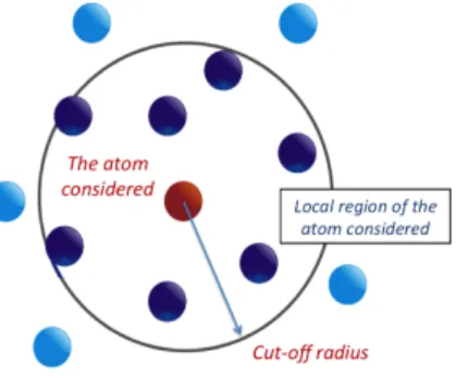
Figure 1: Localization region scheme.
by cubic spline method [1]. These parameters is only fitted for radius range 1.50–5.24 ˚ A, which is correspond to the first four neighbor shells in the diamond structure. Each matrix element will go smoothly to zero between the third and fourth neighbor shells. For matrix elements of Fermi operator f (x), we can calculate directly by Fermi operator expansion [9, 11], as described in Appendix A.
For electronic entropy energy could be calculated by E
ent= −2∆εTr[s(x)]
with
s(x) = − {f (x)lnf (x) + (1 − f (x)) ln (1 − f (x))} .
To construct the matrix elements of s(x), we can use the same procedure as for matrix elements of Fermi f (x) with another set of expansion coefficients. And for repulsive energy, it calculated by
E
rep= X
i,j
1 2 φ(r
ij), where, φ(r) can be obtained also from previous work [10].
For MD implementation, the equation of motion, which is derived from Lagrangian of the system, can be written as
m
id
2r
idt
2= F
i= −2Tr dH
tbdr
if (x)
− d
dr
iE
rep. (5)
Equation of motion as shown in equation (5) is integrated with Verlet algorithm to update the
position and velocity of atoms. During we calculate the force, a localization region (LR) are
introduced, which is associated with each atom. The number of atom will be determined by
cut-off radius r
cutoffof the region (see Figure 1). This feature allow us to reduce the number of
Tight-Binding bases without lossing the accuracy of the calculations. This feature also allow us to
parallelize the calculation because force calculation for each atom is totally independent.
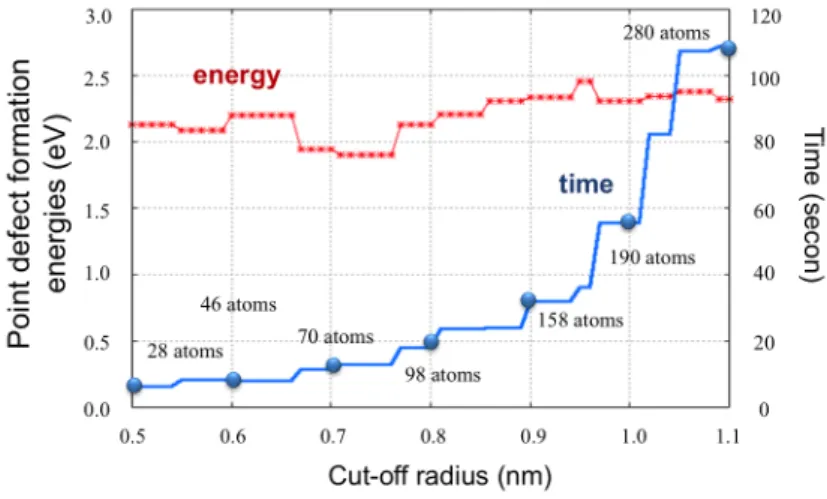
Figure 2: Dependence of cut-off radiusrcutoff to accuracy and time of calculation.
In this investigation, we determine point defect formation energy. Point defect formation energy is important to know the stability of the system while the complete system losses some atom. From previous study [2], point defect formation energy is written by
E
f= E
vacancy−
N − 1 N
E
bulk+ qµ, (6)
where, E
fis point defect formation energy, E
vacancyis total energy of vacancy defect system, E
bulkis total energy of complete system, q is charge, and µ is chemical potential. We use equation (6) to
determine point defect formation energy for several smearing (∆ε). Because of charge neutrality,
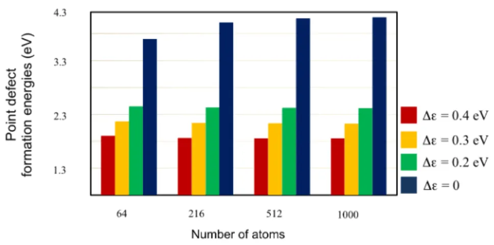
the last part should be neglected. Figure 3 showed us point defect formation energy for several
smearing (∆ε) and also for several size of silicon system: 2 × 2 × 2 (64 atoms), 3 × 3 × 3 (216
atoms), 4 × 4 × 4 (512 atoms), and 5 × 5 × 5 (1000 atoms). When larger smearing is used, we will
get smaller point defect formation energy compare with calculation with small smearing. This case
comes from electronic entropy energy, because when smearing is increase (temperature increase),
possibility to find electrons above Fermi level is also increase. To calculate point defect formation
energy with small smearing, high accuration is required. Degree of polynomial (n
pl) should be
Figure 3: Point defect formation energy for several smearing (∆ε).
Table 1: Point defect formation energies (in eV) in unrelaxed defect configuration.
Our model Lenosky et al. [10] Kwon et al. [3] Ab initio [7]
64 216 512 1000 64 216 64 216
3.645 3.989 4.076 4.102 3.639 3.984 4.720 5.570 4.400
Table 2: Point defect formation energies (in eV) in relaxed defect configuration.
Our model Lenosky et al. [10] Kwon et al. [3] Ab initio [7]
64 216 512 1000 64 216 64 216
3.505 3.801 3.897 4.102 3.949 3.397 3.780 3.390 3.600
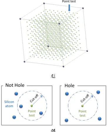
choose a cut-off range associated with each test point. If silicon atom is exist inside the region, the test point will be removed, otherwise will be kept.
(a)
(b)
Figure 4: (a) Test points configuration, (b) Test points selection scheme.
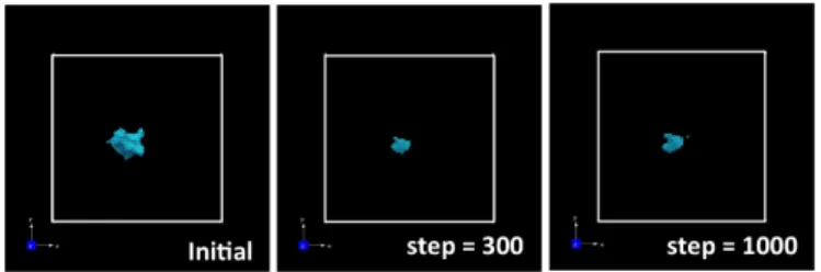
Using this method, we can consider the dynamical behaviors of defects quite easily. As shown
in Figure 5, for liquid state case, the hole will be disappear because atoms near hole will be diffused
8(b), we can see both in liquid state case and non-self-diffusion case, total energies are convergen.
Figure 5: Dynamical behavior of defects in liquid state (1700 K).
Figure 6: Dynamical behavior of defects in non-self-diffusion (1100 K).
4 Summary
TMBD with FEO has been applied to crystal silicon system (with defects) and the results (point defect formation energies) show the value comparable to ab initio result and other previous works.
For Condition of Fermi operator also has been checked. Better result has been obtained, especially when we consider zero temperature case. In this case, however, high degree of polynomial is required to increase the accuracy. To consider behaviors of the defects in multi-vacancy system, a visualization has been constructed. The movement of the hole will be possible to found in non- self-diffusion with long time calculation. For liquid state case, the hole will be disappear because atoms near the hole will be diffuse to fill the hole.
Acknowledgment
The authors would like to JASSO (Japan Student Services Organization) and Beasiswa Unggulan
DIKTI (Ministry of Education and Culture of Indonesia) for finansial support of this research.
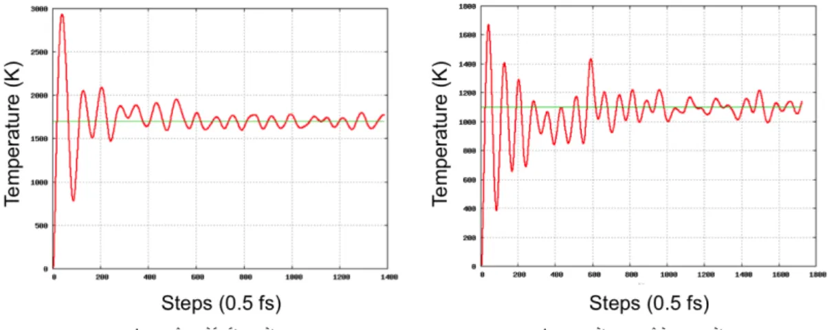
(a) Liquid state case (b) Non-self-diffusion case Figure 7: Time evolution of temperature system.
(a) Liquid state case (b) Non-self-diffusion case
Figure 8: Time evolution of total energy system.
References
[1] A. L. Burden and J. D. Faires (2010). Numerical Analysis, Ninth Edition. Rooks-Cole, Cengage Learning, Boston.
[2] F. Corsetti and A. A. Mostofi (2011). System-size convergence of point defect properties: The case of the silicon vacancy. Phys. Rev. B, 84, 035209.
[3] I. Kwon et al. (1994). Transferable tight-binding models for silicon. Phys. Rev. B, 49, 7242–
7250.
[4] J. C. Slater and G. F. Koster (1954). Simplified LCAO Method for the Periodic Potential Problem. Phys. Rev., 94, 1498–1524.
[5] L. Goodwin, A. J. Skinner, and D. G. Pettifor (1989). Generating transferable tight-binding parameters: application to silicon. Europhys. Lett., 9, 701.
[6] L. Goodwin (1991). A new tight binding parameterization for carbon. J. Phys. Condens.
Matter, 3, 3869.
[7] P. J. Kelly and R. Car (1992). Greens-matrix calculation of total energies of point defects in silicon. Phys. Rev. B, 45, 6543–6563.
[8] S. Goedecker and L. Colombo (1994). Efficient linear scaling algorithm for tight-binding molec- ular dynamics. Phys. Rev. Lett., 73, 122–125.
[9] S. Goedecker and M. Teter (1995). Tight-binding electronic-structure calculations and tight- binding with localized orbital. Phys. Rev. B, 51, 9455–9464.
[10] T. J. Lenosky et al. (1997). Highly optimized tight-binding model of silicon. Phys. Rev. B, 55, 1528–1544.
[11] T. Oda and Y. Hiwatari (2000). Order-N tight-binding molecular dynamics simulation with a
Fermi operator expansion approach: application to a liquid carbon. J. Phys. Condens. Matter,
12, 1627–1639.
2 2
where, x
maxand x
minare the maximum and the minimum eigenvalues of x, respectively. With this scaling, the eigenvalues of t should be in the range between -1 and 1. The degree of polynomial in equation (7), can be chosen by following relation:
n
pl= C W
∆ε
where W ∼ 2∆ε max (x
max, |x
min|) represent a bandwidth of the electronic structure, and C is a constant. For expansion coefficients, it can be obtained by this following formula:
c
j= 2 π
Z
1−1