Kyushu University Institutional Repository
Triplet exciton management towards electrically driven organic lasers
コホナ, パハラ, ワラウェ, ブッディカ, サンジーワ, バンダラ, カルナティ ラカ
http://hdl.handle.net/2324/4110478
出版情報:九州大学, 2020, 博士(工学), 課程博士 バージョン:
権利関係:
2020
Doctoral Dissertation
Triplet exciton management towards electrically driven organic lasers
Kohona Pahala Walawwe Buddhika Sanjeewa Bandara Karunathilaka
Department of Chemistry and Biochemistry Graduate School of Engineering
Kyushu University
Table of contents
Chapter 1
Introduction ... 1
1.1 History of lasers ... 2
1.2 Introduction to organic lasers... 2
1.2.1 Organic semiconductor materials ... 2
1.2.2 Organic laser gain materials... 4
1.2.3 Optically pumped organic lasers ... 6
1.2.4 Organic light-emitting diodes and electrical injection organic semiconductor laser diodes ... 8
1.2.5 Advantages of OSLDs ... 13
1.3 Triplet excitons management in organic laser ... 14
1.3.1 Triplet accumulation ... 14
1.3.2 Short pulse excitation to overcome STA ... 17
1.3.3 Spectral separation to overcome STA ... 18
1.3.4 Triplet management to overcome STA ... 18
1.4 Aim and outline of this thesis ... 20
References ... 21
Chapter 2 An organic laser dye having a small singlet-triplet energy gap makes the selection of a host material easier ... 27
2.1 Introduction ... 28
2.2 Experimental ... 28
2.3 Results and discussion ... 32
2.3.1 Synthesis and characterization ... 32
2.3.2 Photo-physical properties ... 37
2.3.3 ASE properties ... 48
2.3.4 Fabrication of DFB resonators ... 52
2.3.5 Lasing studies in DFB structures under short pulsed excitation ... 54
2.3.6 Lasing studies in DFB structures under CW operation ... 60
2.4 Conclusion ... 65
References ... 65
Chapter 3 Suppression of external quantum efficiency rolloff in organic light-emitting diodes by scavenging triplet excitons ... 67
3.1 Introduction and advantage of using a triplet scavenging host material for EL ... 68
3.2 Experimental ... 69
3.3 Results and discussion ... 72
3.3.1 Frontier molecular orbitals and charge carrier balance in thin-film diodes ... 72
3.3.2 Electrical and electroluminescent properties ... 74
3.3.3 Suppressed EL quenching with long lived excitons ... 77
3.4 Conclusion ... 80
References ... 80
Chapter 4 Summary and perspectives ... 82
4.1 Summary of all Chapters ... 83
4.2 Future perspectives ... 83
4.2.1 From OLED to OSLD ... 83
4.2.2 Prospects of OSLDs ... 85
4.2.3 Future aspects of triplet-management ... 87
References ... 87
Appendix A Fundamentals of DFB lasers ... 90
Chapter 1
Introduction
1.1 History of lasers
The word “laser” is an acronym for “Light Amplification by Stimulated Emission of Radiation”. Albert Einstein in 1917 theoretically proved that the process of stimulated emission must exist[1,2]. In fact, very first amplification of electromagnetic radiation was demonstrated in microwave wavelength, i.e., “Microwave Amplification by Stimulated Emission of Radiation (Maser)[3], by the group of scientists headed by Charles S. Towns in 1954. In 1960, T. H. Maiman of the Hughes Research Laboratories achieved the very first laser action from Ruby crystal in optical frequency[4]. Successively, in 1962, Robert N. Hall demonstrated the first semiconductor laser using Gallium-Arsenide[5]. Since 1962, the development of lasers has been extremely rapid[2,6]. In particular, the very first stimulated emission from an organic material was reported by Sorokin et al. in 1966[7]. Figure 1.1 shows the important milestones in the invention and innovations of laser technology.
Figure 1.1. Significant milestones of laser technology[2,6].
Now, the term of “laser” stands for a device having a gain medium which amplifies light by stimulated emission, a resonator which induces feedback of light (i.e., light travels back and forth through the gain medium) and a pumping source which keeps the population inversion during stimulated emission[8,9].
1.2 Introduction to organic lasers 1.2.1 Organic semiconductor materials
Energy levels of inorganic semiconductors are well explained based on the band
Chapter 1 structures which originate from the properties of crystalline structures of inorganic materials[10]. In general, there are valence and conduction bands which are separated by a forbidden energy gap (bandgap). However, unlike inorganic crystals, organic molecules are usually characterized with molecular orbital theory. Therefore, although there are significant differences in their electronic structures, it is usually assumed that the highest occupied molecular orbital (HOMO) and lowest unoccupied molecular orbital (LUMO) of an organic solid-state are analogous to the valence and conduction bands of an inorganic solid-state, respectively[11–13].
Figure 1.2. Schematic device architectures of conventional (a) inorganic and (b) organic LEDs. Energy-level diagrams of conventional (c) inorganic and (d) organic LEDs. In these figures, EC is the energy level of a conduction band, EF is the energy of a Fermi level, EV is the energy level of a valence band. HIL is the hole injection layer, HTL is the hole transport layer, EML is the emitting layer, ETL is the electron transport layer, and EIL is the electron injection layer.
In addition, here I highlight the difference of electroluminescence (EL) processes between organic and inorganic semiconductors. In inorganic semiconductors, an electron
and a hole recombination occur through the electron transition between the conduction and valence bands, leading to radiative or non-radiative decay with photon or phonon emission respectively (Figure 1.2a,c). In contrast, injected and transported holes and electrons recombine in a molecule, forming an exciton[13] (Figure 1.2b,d) with the branching ratio of 1:3 in singlet and triplet states[14]. Compared to the band-to-band transition in inorganic semiconductors, the exciton generation is the most unique process in organic semiconductors.
1.2.2 Organic laser gain materials
Analogous to a four-level energy scheme of inorganic laser materials, common organic fluorescent materials possess the similar energy diagram[15] (Figure 1.3). In general, internal conversion between vibration energy levels within the same electronic state is faster than the transition between different electronic states. As depicted in Figure 1.3a, the vibrational transitions between E3 to E2, and E1 to E0 are usually in a picosecond regime. The transition between E2 to E1 is either radiative or non-radiative, and this spontaneous transition is called fluorescence emission. Relationship between radiative and non-radiative transitions can be expressed using the following equation:
𝛷𝑃𝐿 = 𝑘𝑟× 𝜏𝑠 = 𝑘𝑟
𝑘𝑟+𝑘𝑛𝑟 (Eq. 1.1)
where, ΦPL, kr, τs and knr are the photoluminescence quantum yield (PLQY), radiative decay constant, fluorescence emission lifetime (corresponding to a lifetime of singlet excited state) and nonradiative decay constant, respectively. As depicted in Figure 1.3b, a fluorescence emission spectrum is a combination of several transitions between the lowest vibrational energy level of the upper electronic state (E2) to several different vibrational states of the ground electronics state (E1). Thus, using a waveguided feed- back resonator, it is possible to isolate one particular transition as the stimulated emission while suppressing other transitions.
Chapter 1
Figure 1.3. (a) Frank-Condon energy level diagram of a four-level organic fluorescent laser gain material. (b) Respective absorption and emission spectra showing vibrational peaks[16].
When the excitation pump energy is increased, the gain of stimulated emission surpasses the optical losses, and then the light amplification begins[15,17]. The minimum required pump energy to begin light amplification is defined as the threshold energy, Eth. The Eth of a slab-waveguide thin film on a low-refractive-index substrate can be expressed as amplified spontaneous emission (ASE) threshold, which is given by;
𝐸𝑡ℎ = 𝐶′ 1
𝛤𝑛𝑒𝑓𝑓𝛷𝑃𝐿(∫𝜎𝜆𝑎𝑑𝜆)−2 (Eq. 1.2)
where C' is a constant, Γ is the confinement factor, neff is the effective refractive index in an emission region, σa is the steady-state absorption cross-section, and λ is the wavelength.
Here, if Eq. 1.3 satisfies;
(∫𝜎𝜆𝑎𝑑𝜆) = 𝑐𝑜𝑛𝑠𝑡𝑎𝑛𝑡 (Eq. 1.3) Then, Eth is inversely proportional to kr as;
𝐸𝑡ℎ ∝ 1 +𝑘𝑛𝑟
𝑘𝑟 (Eq. 1.4)
Therefore, to reduce Eth, we have to use a material with higher PLQY, shorter τs or higher kr[17,18]. There are thousands of organic molecules exhibiting laser characteristics reported from 1966 up to date which have different, unique and special properties based on each class of molecules[11,13,15]. Figure 1.4 shows few common examples of polymers and small
molecules that exhibit light amplification under optical excitation over whole visible region[19,20].
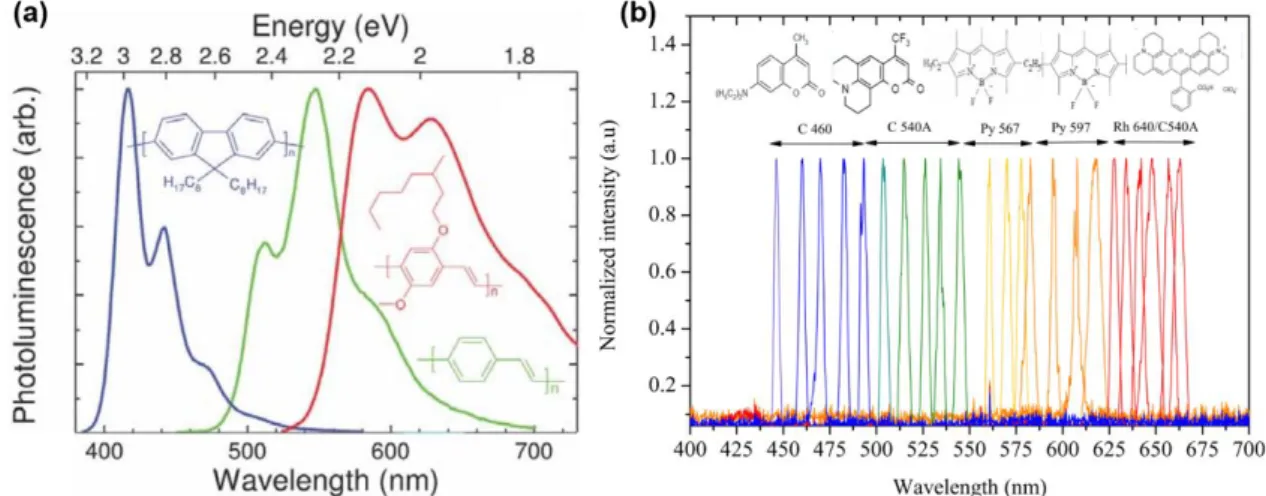
Figure 1.4. (a) Emission spectra of three commonly used conjugated polymers for lasing.
(a-inset) respective polymer structures[21]. (b) Laser spectra of coumarin 460 (C 460, blue solid line), coumarin 540 A (C 540 A, green solid line), pyrromethene 567 (Py 567, light orange solid line), pyrromethene 597 (Py 597, dark orange solid line), and a blend of rhodamine 640 (Rh 640) and C 540 A (red solid line)[22].
1.2.3 Optically pumped organic lasers
After the first demonstration of ASE from an organic material in March 1966[7], Schafer et al. reported the first organic laser in September 1966[23]. Later, the continuous- wave (CW) operation from organic lasers was demonstrated by Peterson et al. in 1970[24]. However, most of the organic lasers used solutions of π-conjugated highly luminescent molecules as the gain medium, which were sometimes inconvenient to solid-state applications[25]. Another organic laser was proposed in 1967[26], with the incorporation of organic laser dyes into solid-state polymeric matrices, indicating that these devices have the benefit to convenient, compact light sources with a low cost[27]. The first organic solid-state semiconductor laser (OSSL) under optical pulse pumping was demonstrated by Hide et al. in 1996[28,29], and the lasing from solid-state conjugated polymer microcavities was also reported by Tessler et al. in the same year[30].
Chapter 1
Figure 1.5. The milestones in the history of breakthrough innovations and inventions of organic lasers.
Subsequently, many researchers then focused on improving the photostability of laser dyes and host matrix molecules to decrease the required pump thresholds under the CW condition and to realize electrically driven organic semiconductor laser diodes (OSLDs)[27,29,31]. The first optically pumped quasi-CW lasers from organic solid-state films were realized by Rabe et al. in 2006[32], and an indirect electrical pumping OSSLs, which otherwise called as a tandem laser diode, was reported by Yang et al. in 2008[33,34]. Further, Sandanayaka et al., demonstrated low threshold surface- emitting OSSLs operating in the quasi-CW regime at 80 MHz as well as under long pulse photo-excitation of 30 ms in 2017[35–37]. Now, true-CW (t-CW) lasing in organic semiconductor films attracts great interest. The milestones in the organic laser history are
summarized in Figure 1.5.
1.2.4 Organic light-emitting diodes and electrical injection organic semiconductor laser diodes
The very first EL from organic materials was reported in 1963 by Pope et al.[38]
and the first practical multi-layered OLEDs were realized in 1986 by Hayashi et al.[39,40]. Later, Tang and Vanslyke demonstrated efficient EL using a bilayer device, which produced high brightness ( > 1000 cd m-2) with the voltage less than 10 V and high external quantum efficiency (EQE) of about 1 %[39]. Then, Adachi et al. reported a fundamental double hetero-architecture consisting of an HTL, an EML and an ETL in 1988[40]. These first-generation OLEDs are referred to as fluorescent OLEDs based on the radiative recombination of singlet excitons. Later, Baldo et al. reported a phosphorescent mechanism, i.e., all singlet excitons rapidly decay to a triplet state by intersystem crossing (ISC) and the generated triplet excitons decay radiatively by employing organometallic compounds such as Ir(ppy)3 in 1998[41]. The devices exploiting such a mechanism are called phosphorescent OLEDs (PHOLEDs) and became the second generation of OLEDs[42]. Later, a very promising alternative mechanism that converts triplet excitons into a singlet state was firstly demonstrated by Adachi group in 2009[43] and their successive studies realized ultimate OLEDs with a high EQE over 20 % by utilizing very efficient triplet up-conversion via reverse-ISC (RISC)[44]. This mechanism is named as thermally activated delayed fluorescence (TADF) and became the third generation of OLEDs as TADF-OLEDs[45,46].
Although the performance of OLEDs has been rapidly developed to the level of practical applications such as displays and lighting, fabricating OSLDs has been a still very difficult task due to Joule heating[47], wave guiding loss[37], quenching of radiative singlets by triplets (singlet-triplet annihilation; STA) or polarons (singlet-polaron
Chapter 1 annihilation; SPA) simultaneously[48–52]. In particular, utilization of organic materials with low laser thresholds is crucial to make the threshold currents lower for OSLDs[53,54].
Figure 1.6. Work done in Adachi laboratory to overcome issues affecting for the realization of current injection OSLDs.
To overcome the aforementioned issues, as shown in Figure 1.6, Adachi laboratory has been developed many organic laser dye materials having low ASE and laser thresholds[55–59] with emission colors ranging from deep blue to near IR regime[59]. Light amplification from a TADF material was also reported in 2017[60]. Degradation mechanism of laser dyes[61] and design strategies of robust laser dyes[62] have been clarified. Molecular orientation of efficient laser gain materials has been investigated in order to get better lasing characteristics[63]. Several device and resonator architectures
were investigated to decrease wave guiding losses of distributed feed-back resonators (DFBs)[20,36,37] in OLED and organic field effect transistor (OFET) structures[57]. Use of short pulse electrical excitation has been investigated in order to drive OLEDs and OSLDs at higher current densities with reduced joule heat[47,53,64]. Using triplet quencher molecules in order to manage triplet excitons and effects of STA has been investigated[35,61,65]. Moreover, laser operation under quasi-CW operation has been demonstrated by Sandanayaka et al.[35–37]. More interestingly, a record-breaking publication about an indication of current injection lasing from OSLDs was reported recently in 2019 by Sandanayaka et al.[53]. Afterward, there are huge attentions has been paid about current excitation and various efforts for reducing the current threshold have been started.
One of the big issues frequently observed in OLEDs is the significant decrease in external quantum efficiency (EQE) at high current densities. This decrease in EQE is termed as “efficiency roll-off”. Major reasons for the efficiency roll-off are triplet induced emission quenching such as STA[37,52,55,66] and SPA. In fact, to suppress roll-off characteristics, it has been clarified that the use of non-heterostructured device architecture leads to suppression of roll-offs (Figure 1.7e), since the heterointerfaces tend to accumulate charge carriers and squeezing the carrier recombination width (Figure 1.7b).
Due to the localization of charge carriers and excitons in organic molecules in case of organic semiconductors, the interaction between charge carriers (radical cations and anions; polarons) and the adjacent molecules is much stronger than that of inorganic compounds. Thus, polaron induced exciton quenching causes serious issues in OSLD performance at higher current densities[53,64]. As shown in Figure 1.7a,c, charge injection in a multilayer device is relatively easier and controllable by combining appropriate HTL and ETL materials. Other advantage of the multilayer devices is charge blocking ability at either side of EML that can confine charges in EML, leading to high efficiency
Chapter 1 (Figure 1.2d and Figure 1.7b)[46]. However, in case of OSLDs, these HTLs and ETLs can yield additional emission quenching sites by the cation and anion absorptions in HTL and ETL, respectively (Figure 1.8), since light travels back and forth between anode and cathode before light is outcoupled[53,64].
Figure 1.7. Schematic of multilayer OLED; (a) hole injection from anode (b) charge hopping and recombination (c) electron injection from cathode. Schematic of single layer OLED; (d) hole injection from anode (e) charge hopping and recombination (f) electron injection from cathode[53,67–70].
Therefore, single layer OLED architecture is vital since we only need to consider about the polaron absorption of an EML material to suppress polaron quenching (Figure 1.7e, Figure 1.8)[53,64]. However, even if the numbers of injected electrons and holes are same, the mobilities of holes and electrons may still be different. Thus, this may lead to non-radiative recombination of holes and electrons near the interface between the injection layer and EML, leading to low efficiency and a high driving voltage[53,67–70]. Specially at high voltages, holes and electrons may drift towards the counter electrodes without recombination each other[47,64]. Therefore, in order to get ideal charge balance in
single layer devices, we have to carefully optimize charge injection and transport characteristics (Figure 1.7d,f)[53,64,71].
Figure 1.8. Various quenching mechanisms affecting to a typical organic laser gain material under current injection; (a) Jablonski energy diagram (b) respective emission and absorption spectra. CR, CS, VR and ISC stands for charge separation, charge recombination, vibrational relaxation and intersystem crossing respectively.
1.2.5 Advantages of OSLDs
Lasers have extremely unique and useful properties such as high intensity, directionality, monochromatic emission, and coherence. Due to these properties, lasers have found applications in almost every industrial sector, for example, in scanners,
Chapter 1 printers, and sensors. Until now, lasers for these applications are typically based on inorganic materials which are generally brittle, nonflexible, and high cost processing[8,17]. In contrast to inorganic semiconductors, organic semiconductor materials are generally easier to process, and the resulting devices can be mechanically flexible. Thus, lasing from organic semiconductor materials can be used for a wide range of applications such as displays[72], lighting[29,31], sensors[73], optical communications[74,75] and spectroscopy[31]. Interestingly, OLEDs paved the way to curved displays which are commercially available now. Pixels in those displays outcouples light with Lambertian distribution. However, if we can make those pixels with OSLDs which outcouple highly directional laser light, OSLDs can pioneer new applications such as curved holographic displays that can create virtual objects in 3D space outside of the display plane[76–79].
Figure 1.9. Potential applications of current injection OSLDs.
Moreover, due to the ultimate opportunities to change the molecular structures of lasing materials, we can tune the emission wavelength[27] and may optimize the material stability[62], crystallinity, PLQY and electronic energy levels[80]. In addition, organic emitter materials are often biodegradable, and devices based on them will be
environmental-friendly. Due to their facile processability, they are compatible with a large variety of optical resonator structures and, in many cases, the resonator can be inscribed directly into the organic gain medium, leading to versatile and relatively low-cost laser devices. Few examples for future potential applications of current injection OSLD is given in Figure 1.9.
1.3 Triplet excitons management in organic laser 1.3.1 Triplet accumulation
Regarding organic laser materials, the formation of long-lived triplet excitons and triplet accumulation is one of the major disadvantages. The population of triplet excitons mainly depends on the rates of triplet formation and relaxation (Figure 1.10a,b).
In a pristine film, the rate of triplet exciton formation solely depends on the rate of intersystem crossing (ISC) from a singlet state to a triplet state which is an intrinsic property of the molecule. However, as shown in Figure 1.10a, in case of a guest-host system, the rate of triplet exciton formation depends on triplet sensitization and the molar ratio. On the other hand, under electrical excitation, triplets are formed on emitter molecules either as direct exciton formation by charge recombination on emitter molecules or as triplet sensitizing by host molecules in a guest-host system (Figure 1.10b).
Therefore, with an increase of current density, the rate of triplet formation significantly increases due to the branching ratio of singlets and triplets (1:3)[14]. Therefore, at high current densities, triplet accumulation and triplet induced losses can be a serious problem in OSLDs and decrease the operational durability[61].
Chapter 1
Figure 1.10. Rate of exciton dynamics related to triplet accumulation; (a) optical excitation (b) electrical excitation. Calculated exciton density versus long pulsed electrical excitation in a guest-host film at a current density of 1 kA/cm2; (c) without (d) with considering electric field across the electrodes. The closed symbols indicate the dynamics for the low kTTA of the host:guest system. The open symbols (dashed lines) have been calculated with a TTA rate of kTTA = 5.0 × 10⁻¹³ cm3 s-1.[81]
As shown in Figure 1.10c,d Kasemann et al. calculated, singlet and triplet population of 40 nm thick 2 wt.% 4-dicyanomethylene-2-methyl-6-p- dimethylaminostyryl-4H-pyran (DCM) in tris(8-hydroxyquinoline) (Alq3) guest:host film under electrical excitation at 1 kA cm-2. Figure 1.10c shows the population when the electron mobility is 1×10⁻⁵ cm2 V-1 s-1 and Figure 1.10d shows the population when the electron mobility is 2×10⁻⁴ cm2 V-1 s-1. The results clearly showing the population of triplets are increasing with excitation time, while singlet exciton population is decreasing, and the behavior is more severe under high current mobilities[81–83]. Thus, these accumulated triplets can hamper light amplification by singlet excitons even without
annihilation processes. Moreover, the open symbols with dashed lines in Figure 1.10d shows when a triplet-triplet annihilation (TTA) mechanism involved in, the population of singlets could increase while decreasing the population of triplets[81].
The accumulated triplets will induce two major exciton quenching processes, i.e., STA and TTA. Note that quenching of singlet excitons by other singlet excitons [singlet- singlet annihilation (SSA)], quenching of singlet excitons by polarons (SPA), Joule heating [singlet-heat quenching (SHQ)][84], electric field induced quenching are other exciton quenching mechanisms of singlets which are not induced by triplet excitons.
Here, I explain STA and TTA processes in more detail. In the event of TTA, the collision of two excited state triplets (T1) in the absence of a magnetic field may result in one ground state singlet molecule and nine equally probable statistical outcomes of excited state molecules, one of which is singlet (Sn), three are triplets (Tn) and five are quintets (Qn) which can represent by following Eq. 1.5;
𝑇1+ 𝑇1 → 𝑆0+1
9𝑆𝑛+3
9𝑇𝑛 +5
9𝑄𝑛 (Eq. 1.5)
Here, the event of TTA requires close proximity of two triplet excitons by high triplet exciton density, thus this is a bimolecular Dexter energy transfer (DET) process.
TTA is relatively significant at high current densities of electrical excitation due to 75 % triplet formation efficiency. Low doping ratio of triplet accumulating molecules in a blend can increase the distance between triplet excitons, thus it decreases the DET efficiency for TTA. Interestingly, a TTA process can yields singlet excitons after the annihilation process, leading to the enhancement of EL efficiency in case of fluorescence emitters[85–
90].
On the other hand, quenching of singlets by long-lived triplets, which is known as STA (Figure 1.11a), is the most serious triplet induced quenching process for organic lasers[52,81,91–95]. When the singlet emission (S1-S0 energy gap) of a donor molecule is
Chapter 1 approximately equal to the triplet absorption (T1-Tn energy gap) of an accepter molecule, the STA takes place (Figure 1.11a). Since this is a Förster resonance energy transfer (FRET) process, a long-range energy transfer is possible at STA. Moreover, since triplet population is three times larger than singlet population at electrical excitation, STA is much more severe and detrimental. Thus, as explained in section 1.2.4, the major cause for the efficiency rolloff in OLEDs is STA[37,52,55,66].
Figure 1.11. Schematic exciton energy transfer mechanism of STA; (a) Energy level diagram, (b) molecular orbital diagram. Abs, ISC, FRET and TA stands for steady state absorption, intersystem crossing, Förster resonance energy transfer and triplet absorption respectively.
1.3.2 Short pulse excitation to overcome STA
Since triplet lifetime is longer than singlet lifetime, using long pulse excitation increases the population density of triplets (Figure 1.10). Therefore, one way to suppress the triplet accumulation is to use optically and electrically short-pulse excitation (nanoseconds or lower) with longer rest time (low pulse frequency). Thus, shorter pulse excitation leads smaller triplet population and those triplets relax to a ground state after longer relaxation time. In addition, this short-pulsed excitation helps to dissipate joule heat and thereby increase device stability. However, there are plenty of organic materials that show lasing under a short-pulsed optical excitation but do not show lasing under long pulse or CW optical excitation.
1.3.3 Spectral separation to overcome STA
One way to suppress the STA is to design and synthesis organic emitters, which have no spectral overlap between the singlet emission (S1-S0) and the triplet absorption (T1-Tn). The FRET efficiency between singlet and triplet excitons will be minimized (Figure 1.11a). Therefore, as depicted in Figure 1.12, strong STA can be observed when there is the large spectral overlap. There are few molecules such as 4-4΄-bis[(N- carbazole)styryl]biphenyl (BSBCz)[36,53,96,97] and ter(9,9'-spirobifluorene) (TSBF)[55]
which satisfy this condition[52,92,98]. Moreover, even though no spectral overlap could completely overcome STA, it is hard to avoid triplet accumulation on emitter molecules specially under CW operation and electrical excitation.
Figure 1.12. Depicts three representative cases of an organic compounds that exhibits (A) strong (B) moderate and (C) small FRET efficiencies of STA. S-S denotes steady state singlet-singlet absorption, FL denotes fluorescence emission from S1 to S0 and T-T denotes excited state triplet-triplet absorption from T1 to Tn.[52]
1.3.4 Triplet management to overcome STA
Another intrinsic way to manage triplet excitons can be realized by blending organic emitters with triplet manager molecules[93,99,100]. In this case, it is important to consider the spectral overlap of the singlet emission of an emitter molecule and the triplet
Chapter 1 excited-state absorption of a scavenger molecule, because this spectral overlap causes the STA between them. To have efficient triplet scavenging, the triplet manager molecule should meet a set of important requirements[101];
1) Triplet manager should be able to accept a triplet exciton from the emitter molecules, implying that the triplet energy level of a triplet manager molecule should be low enough than that of the emitter.
2) At the same time, the singlet energy level of a triplet manager should be high enough to prevent quenching of singlet excitons of the emitter molecules. This implies that the S1–T1 splitting for the triplet manager should be enough large.
3) Triplet manager should possess a reasonably short intrinsic triplet lifetime to quickly deplete the triplet population so that triplet accumulation would not happen.
4) It should have the spectral separation between the emission region and the excited state absorption, i.e., triplet absorption (TA), polaron absorption (PA) of triplet managers.
5) Triplet manager should not enhance ISC of the emitter molecules to prevent converting singlets into triplet excitons. This criterion imposes certain limitations for employing compounds containing heavy atoms (such as metal–organic complexes) as triplet managers[101,102].
Mostly, triplet oxygen[65,100], perylene derivatives[103], cyclooctatetraene (COT)[101,104], and anthracene derivatives[101,105–107] have been used as triplet managers in previous studies. However, in most of these scenarios, the triplet managers are either in gas phase or in solid-state with high crystallinity, which implies that those cannot be used as an efficient host material. Therefore, finding such materials, which possess requirements for a host as well as requirements for a triplet scavenger, is rather hard[101].
In general, a good host molecule should possess the following set of important requirements[108–110];
1) Effective spectral overlap between the emission spectra of a host molecule and the absorption spectra of an emitter molecule, thereby having efficient forward FRET.
2) Bipolar charge transport properties for use in electrical operation.
3) Crystallization should be minimum so that the charge accumulation and light scattering at grain boundaries can be minimized.
4) It should not form degenerated energy states at the aggregation of host molecules such as excimer or dimer states.
5) It should not form an exciplex with an emitter molecule to avoid any degenerated energy states.
6) It should have proper matching of highest occupied molecular orbital (HOMO) and lowest unoccupied molecular orbital (LUMO) levels compatible with an emitter molecule and electrodes for use in electrical operation.
1.4 Aim and outline of this thesis
Although it is obvious that organic lasers have many advantages as a potential alternative[58] to inorganic semiconductor lasers, organic lasers have to overcome several issues to realize high performance CW lasing[24,111–114] and current injection organic lasers[48,50,53]. Major obstacles of organic laser materials for enhancing laser device performance originate from the accumulation of triplet excitons which lead to various deactivation effects such as STA.
In this thesis, instead of designing a molecule with all requirements for a triplet scavenger and for a host molecule, I selected a fluorescent material having a small singlet- triplet energy gap (ΔEST). Hence, the triplets of a guest emitter are easily transferred to a
Chapter 1 host material, realizing efficient removal of triplets from emitter molecules. In Chapter 2, the proposed strategy is proved by incorporating a novel fluorescent emitter having a rather small ΔEST into a host layer having efficient triplet scavenging capability. Then, the proposed guest-host matrix is embedded into a DFB architecture to demonstrate optically driven CW lasers. Based on the promising result under optical excitation, Chapter 3 demonstrate the suppression of efficiency roll-off at high current densities and long-pulse excitation in the OLED. Chapter 4 summarizes this thesis and discuss future perspectives. Finally, fundamentals of DFB lasers are discussed in Appendix A, to clarify optical physics behind DFB optical resonators, and its usage for integrated organic lasers.
References
[1] A. Einstein, Physiol Z 1917, 18, 121.
[2] M. Rose and H. Hogan, A History of the Laser : 1960 – 2019, Available at:
https://www.photonics.com/Articles/A_History_of_the_Laser_1960_- _2019/a42279.
[3] A. L. Schawlow and C. H. Townes, Phys. Rev. 1958, 112, 1940.
[4] T. H. Maiman, Nature 1960, 187, 493.
[5] R. N. Hall, G. E. Fenner, J. D. Kingsley, T. J. Soltys, R. O. Carlson, Phys. Rev. Lett.
1962, 9, 366.
[6] On the shoulders of giants. Photonics media 2019, Available at:
https://www.photonics.com/Article.aspx?AID=42280.
[7] P. P. Sorokin, J. R. Lankard, IBM J. Res. Dev. 1966, 10, 162.
[8] W. F. Coleman, J. Chem. Educ. 1982, 59, 441.
[9] R. M. Herd, J. S. Dover, K. A. Arndt, Dermatol. Clin. 1997, 15, 355.
[10] R. Dabu, Crystals 2019, 9, 347.
[11] R. Goyena and A. Fallis, Hand book of organic materials for optical and (opto)electronic devices; Woodhead Publishing Series in Electronic and Optical Materials:, 2013; Vol. 39, pp. 17.
[12] A. Köhler, H. Bässler, Mater. Sci. Eng. R Reports 2009, 66, 71.
[13] Z. Li, H. Meng, Organic Light Emitting Materials and Devices; Taylor & Francis Group, 2007; pp. 12.
[14] M. A. Baldo, D. F. O’Brien, M. E. Thompson, S. R. Forrest, Phys. Rev. B - Condens.
Matter Mater. Phys. 1999, 60, 14422.
[15] M. Anni, S. Lattante, Organic Lasers Fundamentals, Developments and Application; Pan Stanford Publishing Pte. Ltd., 2018; pp. 6.
[16] Wikimedia Commons contributors, File:Vibration-fluor-abs.png. Wikimedia Commons, Free media Repos, DOI:361032222.
[17] W. T. Silfvast, Fundamentals of Photonics; Lasers (Module 5 of 10). Mater. Dev.
under Proj. STEP (Scientific Technol. Educ. Photonics) by Univ. Connect. CORD 2003; pp. 5.
[18] H. Ye, Development of deep-red and near-infrared organic luminescent materials and their applications in organic light-emitting diodes and continuous-wave organic semiconductor lasers. Doctoral thesis, Graduate School of Engineering Kyushu University, 2019.
[19] H. Xia, C. Hu, T. Chen, D. Hu, M. Zhang, K. Xie, Polymers (Basel) 2019, 11(3),433.
[20] J. H. Kim, M. Inoue, L. Zhao, T. Komino, S. Seo, J. C. Ribierre, C. Adachi, Appl.
Phys. Lett. 2015, 106, 053302.
[21] I. D. W. Samuel, G. A. Turnbull, Mater. Today 2004, 7(9), 28.
[22] O. Mhibik, T. Leang, A. Siove, S. Forget, S. Chénais, Appl. Phys. Lett. 2013, 102, 041112.
[23] F. P. Schäfer, W. Schmidt, J. Volze, Appl. Phys. Lett. 1966, 9, 306.
[24] O. G. Peterson, S. A. Tuccio, B. B. Snavely, Appl. Phys. Lett. 1970, 17, 245.
[25] D. Strickland, G. Mourou, Opt. Commun. 1985, 56, 219.
[26] B. H. Soffer, B. B. McFarland, Appl. Phys. Lett. 1967, 10, 266.
[27] I. D. W. Samuel, G. A. Turnbull, Chem. Rev. 2007, 107, 1272.
[28] M. A. Díaz-García, F. Hide, B. J. Schwartz, M. D. McGehee, M. R. Andersson, A.
J. Heeger, Appl. Phys. Lett. 1997, 70, 3191.
[29] A. J. C. Kuehne, M. C. Gather, Chem. Rev. 2016, 116, 12823.
[30] N. Tessler, G. J. Denton, R. H. Friend, Nature 1996, 382, 695.
[31] S. Chénais, S. Forget, Polym. Int. 2012, 61, 390.
[32] T. Rabe, K. Gerlach, T. Riedl, H. H. Johannes, W. Kowalsky, J. Niederhofer, W.
Gries, J. Wang, T. Weimann, P. Hinze, F. Galbrecht, U. Scherf, Appl. Phys. Lett.
2006, 89, 87.
[33] Y. Yang, G. A. Turnbull, I. D. W. Samuel, Appl. Phys. Lett. 2008, 92, 92.
[34] F. J. Duarte, L. S. Liao, K. M. Vaeth, Opt. Lett. 2005, 30, 3072.
[35] A. S. D. Sandanayaka, L. Zhao, D. Pitrat, J. C. Mulatier, T. Matsushima, C.
Andraud, J. H. Kim, J. C. Ribierre, C. Adachi, Appl. Phys. Lett. 2016, 108, 223301.
[36] A. S. D. Sandanayaka, T. Matsushima, F. Bencheikh, K. Yoshida, M. Inoue, T.
Fujihara, K. Goushi, J. C. Ribierre, C. Adachi, Sci. Adv. 2017, 3(4), e1602570.
[37] A. S. D. Sandanayaka, K. Yoshida, M. Inoue, C. Qin, K. Goushi, J. C. Ribierre, T.
Matsushima, C. Adachi, Adv. Opt. Mater. 2016, 4(6), 834.
Chapter 1 [38] M. Pope, H. P. Kallmann, P. Magnante, J. Chem. Phys. 1963, 38, 2042.
[39] C. W. Tang, S. A. Vanslyke, Appl. Phys. Lett. 1987, 51, 913.
[40] C. Adachi, S. Tokito, T. Tsutsui, S. Saito, Jpn. J. Appl. Phys. 1988, 27, 269.
[41] M. A. Baldo, D. F. O’Brien, Y. You, A. Shoustikov, S. Sibley, M. E. Thompson, S.
R. Forrest, Nature 1998, 395, 151.
[42] C. Adachi, M. A. Baldo, M. E. Thompson, S. R. Forrest, J. Appl. Phys. 2001, 90, 5048.
[43] A. Endo, M. Ogasawara, A. Takahashi, D. Yokoyama, Y. Kato, C. Adachi, Adv.
Mater. 2009, 21, 4802.
[44] H. Uoyama, K. Goushi, K. Shizu, H. Nomura, C. Adachi, Nature 2012, 492, 234.
[45] F. B. Dias, T. J. Penfold, A. P. Monkman, Methods Appl. Fluoresc. 2017, 5, 012001.
[46] H. Nakanotani, K. Masui, J. Nishide, T. Shibata, C. Adachi, Sci. Rep. 2013, 3, 2127.
[47] H. Nakanotani, T. Oyamada, Y. Kawamura, H. Sasabe, C. Adachi, Japanese J. Appl.
Physics, Part 1 Regul. Pap. Short Notes Rev. Pap. 2005, 44, 3659.
[48] M. A. Baldo, R. J. Holmes, S. R. Forrest, Phys. Rev. B - Condens. Matter Mater.
Phys. 2002, 66, 353211.
[49] S. Z. Bisri, T. Takenobu, Y. Iwasa, J. Mater. Chem. C 2014, 2, 2827.
[50] M. Chakaroun, A. Coens, N. Fabre, F. Gourdon, J. Solard, A. Fischer, A. Boudrioua, C. C. Lee, Opt. Express 2011, 19(2), 493.
[51] F. J. Duarte, K. M. Vaeth, Chapter 11; Electrically-pumped organic semiconductor laser emission, Organic Lasers and Organic Photonics; IOP Publishing, 2018; pp.
2053-2563.
[52] T. G. Pavlopoulos, Prog. Quantum Electron. 2002, 26, 193.
[53] A. S. D. Sandanayaka, T. Matsushima, F. Bencheikh, S. Terakawa, W. J.
Potscavage, C. Qin, T. Fujihara, K. Goushi, J. C. Ribierre, C. Adachi, Appl. Phys.
Express 2019, 12, 061010.
[54] J. Lin, Y. Hu, Y. Lv, X. Guo, X. Liu, Sci. Bull. 2017, 62, 1637.
[55] M. Inoue, T. Matsushima, C. Adachi, Appl. Phys. Lett. 2016, 108, 133302.
[56] D. H. Kim, A. S. D. Sandanayaka, L. Zhao, D. Pitrat, J. C. Mulatier, T. Matsushima, C. Andraud, J. C. Ribierre, C. Adachi, Appl. Phys. Lett. 2017, 110, 023303.
[57] H. Nakanotani, S. Akiyama, D. Ohnishi, M. Moriwake, M. Yahiro, T. Yoshihara, S. Tobita, C. Adachi, Adv. Funct. Mater. 2007, 17, 2328.
[58] V. T. N. Mai, A. Shukla, M. Mamada, S. Maedera, P. E. Shaw, J. Sobus, I. Allison, C. Adachi, E. B. Namdas, S. C. Lo, ACS Photonics 2018, 5, 4447.
[59] A. D’Aléo, M. H. Sazzad, D. H. Kim, E. Y. Choi, J. W. Wu, G. Canard, F. Fages, J.-C. Ribierre, C. Adachi, Chem. Commun. 2017, 53, 7003.
[60] H. Nakanotani, T. Furukawa, T. Hosokai, T. Hatakeyama, C. Adachi, Adv. Opt.
Mater. 2017, 5(12), 1700051.
[61] T. Matsushima, S. Yoshida, K. Inada, Y. Esaki, T. Fukunaga, H. Mieno, N.
Nakamura, F. Bencheikh, M. R. Leyden, R. Komatsu, C. Qin, A. S. D.
Sandanayaka, C. Adachi, Adv. Funct. Mater. 2019, 29, 1807148.
[62] Y. Oyama, M. Mamada, A. Shukla, E. G. Moore, S.-C. Lo, E. B. Namdas, C.
Adachi, ACS Mater. Lett. 2020, 2, 161.
[63] D. Yokoyama, A. Sakaguchi, M. Suzuki, C. Adachi, Org. Electron. 2009, 10(1), 127.
[64] F. Bencheikh, A. S. D. Sandanayaka, T. Fukunaga, T. Matsushima, C. Adachi, 2019, 126, 185501.
[65] L. Zhao, M. Inoue, K. Yoshida, A. S. D. Sandanayaka, J. H. Kim, J. C. Ribierre, C.
Adachi, IEEE J. Sel. Top. Quantum Electron. 2016, 22, 26.
[66] C. Murawski, K. Leo, M. C. Gather, Adv. Mater. 2013, 25, 6801.
[67] C. Poriel, J. Rault-Berthelot, Adv. Funct. Mater. 2020, 30(17), 1910040.
[68] Z. Wu, Z. Yang, K. Xue, C. Fei, F. Wang, M. Yan, H. Zhang, D. Ma, W. Huang, RSC Adv. 2018, 8, 11255.
[69] N. B. Kotadiya, P. W. M. Blom, G. J. A. H. Wetzelaer, Nat. Photonics 2019, 13, 765.
[70] X. Kai, Y. Minnan, P. Fei, T. Mengying, P. Xudong, Z. Hongmei, Acta Phys. - Chim.
Sin. 2019, 35, 896.
[71] I. D. W. Samuel, E. B. Namdas, G. A. Turnbull, Nat. Photonics 2009, 3, 546.
[72] J. Zhao, Y. Yan, Z. Gao, Y. Du, H. Dong, J. Yao, Y. S. Zhao, Nat. Commun. 2019, 10, 870.
[73] A. Rose, Z. Zhu, C. F. Madigan, T. M. Swager, V. Bulović, Nature 2005, 434, 876.
[74] D. A. Vithanage, P. P. Manousiadis, M. T. Sajjad, S. Rajbhandari, H. Chun, C.
Orofino, D. Cortizo-Lacalle, A. L. Kanibolotsky, G. Faulkner, N. J. Findlay, D. C.
O’Brien, P. J. Skabara, I. D. W. Samuel, G. A. Turnbull, Appl. Phys. Lett. 2016, 109, 013302.
[75] J. Clark, G. Lanzani, Nat. Photonics 2010, 4, 438.
[76] J. Hahn, H. Kim, Y. Lim, G. Park, B. Lee, Opt. Express 2008, 16, 12379.
[77] M. Guillaumee, S. P. Vahdati, E. Tremblay, A. Mader, G. Bernasconi, V. J. Cadarso, J. Grossenbacher, J. Brugger, R. Sprague, C. Moser, IEEE/OSA J. Disp. Technol.
2014, 10, 444.
[78] J. Park, K. R. Lee, Y. K. Park, Nat. Commun. 2019, 10, 1304.
[79] W. Wan, W. Qiao, D. Pu, R. Li, C. Wang, Y. Hu, H. Duan, L. J. Guo, L. Chen, iScience 2020, 23, 100773.
[80] M. Goossens, A. Ruseckas, G. A. Turnbull, I. D. W. Samuel, Appl. Phys. Lett. 2004, 85, 31.
[81] D. Kasemann, R. Brückner, H. Fröb, K. Leo, Phys. Rev. B 2011, 84, 115208.
[82] T. Hori, K. Totani, S. Hirata, T. Watanabe, Chem. Phys. Lett. 2018, 704, 5.
[83] S. Hirata, M. Vacha, Adv. Opt. Mater. 2016, 4, 297.
Chapter 1 [84] K. Yoshida, T. Matsushima, Y. Shiihara, H. Kuwae, J. Mizuno, C. Adachi, J. Appl.
Phys. 2017, 121.
[85] N. Chitraningrum, T. Y. Chu, P. T. Huang, T. C. Wen, T. F. Guo, Org. Electron.
2018, 62, 505.
[86] A. S. Gertsen, M. Koerstz, K. V. Mikkelsen, Phys. Chem. Chem. Phys. 2018, 20, 12182.
[87] R. R. Islangulov, D. V. Kozlov, F. N. Castellano, Chem. Commun. 2005, 1, 3776.
[88] J. E. Auckett, Y. Y. Chen, T. Khoury, R. G. C. R. Clady, N. J. Ekins-Daukes, M. J.
Crossley, T. W. Schmidt, J. Phys. Conf. Ser. 2009, 185, 6.
[89] D. Y. Kondakov, Philos. Trans. R. Soc. A Math. Phys. Eng. Sci. 2015, 373.
[90] J. Saltiel, G. R. Marchand, W. K. Smothers, S. A. Stout, J. L. Charlton, J. Am. Chem.
Soc. 1981, 103, 7159.
[91] Y. Zhang, M. Whited, M. E. Thompson, S. R. Forrest, Chem. Phys. Lett. 2010, 495, 161.
[92] M. Lehnhardt, T. Riedl, T. Weimann, W. Kowalsky, Phys. Rev. B 2010, 81, 165206.
[93] Y. Zhang, S. R. Forrest, Phys. Rev. B 2011, 84, 241301.
[94] E. B. Namdas, A. Ruseckas, I. D. W. Samuel, S. C. Lo, P. L. Burn, Appl. Phys. Lett.
2005, 86, 091104.
[95] A. Dey, N. Chandrasekaran, D. Chakraborty, P. Johari, C. R. McNeill, A. Rao, D.
Kabra, npj Flex Electron. 2018, 2, 28.
[96] H. Nakanotani, C. Adachi, S. Watanabe, R. Katoh, Appl. Phys. Lett. 2007, 90, 4.
[97] T. Aimono, Y. Kawamura, K. Goushi, H. Yamamoto, H. Sasabe, C. Adachi, Appl.
Phys. Lett. 2005, 86, 071110.
[98] C. Xiang, X. Fu, W. Wei, R. Liu, Y. Zhang, V. Balema, B. Nelson, F. So, Adv. Funct.
Mater. 2016, 26, 1463.
[99] A. Salehi, C. Dong, D. H. Shin, L. Zhu, C. Papa, A. Thy Bui, F. N. Castellano, F.
So, Nat. Commun. 2019, 10, 2305.
[100] M. Inoue, T. Matsushima, H. Nakanotani, C. Adachi, Chem. Phys. Lett. 2015, 624, 43.
[101] S. Schols, A. Kadashchuk, P. Heremans, A. Helfer, U. Scherf, ChemPhysChem 2009, 10, 1071.
[102] A. Dey, D. Kabra, J. Phys. Chem. A 2019, 123, 4858.
[103] M. Ahmad, M. D. Rahn, T. A. King, Appl. Opt. 1999, 38, 6337.
[104] T. N. Das, K. I. Priyadarsini, J. Chem. Soc. Faraday Trans. 1994, 90, 963.
[105] S. Schols, A. Kadashchuk, P. Heremans, A. Helfer, U. Scherf, In Organic Light Emitting Materials and Devices XIII; So, F.; Adachi, C., Eds.; SPIE, 2009; Vol.
7415, pp. 43.
[106] Y. Zhang, M. Slootsky, S. R. Forrest, in Conference on Lasers and Electro-Optics 2012, OSA Technical Digest, 2012, paper CW1L.6.
[107] Y. J. Pu, G. Nakata, F. Satoh, H. Sasabe, D. Yokoyama, J. Kido, Adv. Mater. 2012, 24, 1765.
[108] X. Ren, J. Li, R. J. Holmes, P. I. Djurovich, S. R. Forrest, M. E. Thompson, Chem.
Mater. 2004, 16, 4743.
[109] C. Han, Y. Zhao, H. Xu, J. Chen, Z. Deng, D. Ma, Q. Li, P. Yan, Chem. - A Eur. J.
2011, 17, 5800.
[110] S. Gong, X. He, Y. Chen, Z. Jiang, C. Zhong, D. Ma, J. Qin, C. Yang, J. Mater.
Chem. 2012, 22, 2894.
[111] T. Rabe, K. Gerlach, T. Riedl, H. H. Johannes, W. Kowalsky, J. Niederhofer, W.
Gries, J. Wang, T. Weimann, P. Hinze, F. Galbrecht, U. Scherf, Appl. Phys. Lett.
2006, 89, 081115.
[112] R. Bornemann, U. Lemmer, E. Thiel, Opt. Lett. 2006, 31, 1669.
[113] P. Brenner, O. Bar-On, M. Jakoby, I. Allegro, B. S. Richards, U. W. Paetzold, I. A.
Howard, J. Scheuer, U. Lemmer, Nat. Commun. 2019, 10, 988.
[114] T. Riedl, In 2015 European Conference on Lasers and Electro-Optics - European Quantum Electronics Conference, 2015, paper CE_8_1.
Chapter 2
An organic laser dye having a small singlet-triplet energy gap
makes the selection of a host material easier
- 28 - 2.1 Introduction
In this Chapter, I proposed and proved an ideal lasing system that induces efficient triplet scavenging by developing a novel laser material having a rather small singlet-triplet energy gap (ΔEST) which promotes efficient triplet energy transfer from a guest to a host while the single energy transfer only occurs from a host to a guest. Here, I synthesized a promising lasing molecule of 2,6-dicyano-1,1-diphenyl-λ5σ4-phosphinine (DCNP) based on the synthesis route reported by N. Hashimoto et al.[1]. I used DCNP as a laser dye and BSBCz as a triplet scavenging host to realize a stable green organic laser.
Since the triplet exciton formed on DCNP is easily transferred to BSBCz, I was able to eliminate the triplet-induced losses. Here, the excited state absorption spectrum of BSBCz[2–4] does not seriously overlap with the laser emission spectrum of DCNP. In addition, BSBCz as a triplet-scavenging-host molecule fulfills most of the requirements described in Chapter 1, such as a high S1 than that of the emitter, a low T1 than that of the emitter, faster nonradiative relaxation from the T1, no heavy metals, no serious crystallization, bipolar charge transport characteristics, matching HOMO and LUMO levels, and the capability of vacuum deposition. By taking these advantages, in this Chapter, I realized high performance from an optically pumped laser system based on DCNP-doped BSBCz films.
2.2 Experimental
Synthesis and molecular characterization of DCNP
Detail methods and explanation are given in section 2.3.1.
Organic film fabrication
DCNP, BSBCz neat films and 0.5, 1, 2, 4, 8 wt.%-DCNP doped BSBCz films each with a thickness of 200 nm were fabricated on clean fused quartz substrates by vacuum deposition under a pressure of 2×10⁻⁴ Pa. The deposition rate was set at
Chapter 2
- 29 -
0.25 nm s−1. These films were transferred directly into a nitrogen-filled glove box without exposure to air and then encapsulated using a sapphire plate and transparent fluoropolymer CYTOP® as reported previously[3]. PMMA films doped with DCNP at 0.1, 0.3, 0.5, 1, 2, 3, 4, 5, 6, and 8 wt.%, each with a thickness of approximately 200 nm, were also prepared using a spin-coating method for comparison.
Photo-physical characterization
Steady-state absorption spectra, PL spectra and PL quantum yields of the aforementioned films were measured using a double beam absorption spectrometer (Lambda 950, Perkin Elmer), a spectro- fluorometer (FP 8600 by JASCO) and an absolute PL quantum yield measurement system (Quantaurus-QY plus, Hamamatsu Photonics), respectively. Time-resolved PL decays were measured using a transient emission spectrometry setup, in which the excitation source was; Nd:YAG/YVO laser (EKSPLA PL-2250, third harmonic wave generation) with an excitation wavelength of 355 nm and pulse duration of 30 ps and the detector was a streak camera (C10910-01, Hamamatsu Photonics). Excited-state absorption spectra were measured using two separate transient absorption setups designed for ns and μs time scales. The measurement with the ns-time scale was taken using the same excitation laser source used for transient emission measurement by coupled with a Xe lamp and streak camera (C7700, Hamamatsu Photonics). The measurement at the μs time scale was taken using third-harmonic-wave laser light from a Nd:YAG laser with a wavelength of 355 nm (Quanta-Ray GCR-130, Spectra-Physics) as the pump light, and pulsed white light from a Xe lamp as the probe light and the streak camera (C7700, Hamamatsu Photonics) as the detector. The ionization energies of BSBCz and 1 wt.%-DCNP:BSBCz films were measured using photoelectron yield spectroscopy (AC-3, Riken Keiki).
ASE characterization
200 nm thick films were prepared on quartz substrates. For the ASE
- 30 -
measurements, pulsed excitation light from a N2 laser (KEN-2020, Usho) was focused on the edge of the films in a stripe shaped irradiation area of 0.12×0.32 cm2 using a lens and slit. For the pulsed excitation, an excitation wavelength was 337 nm, pulse width was 0.8 ns, and repetition rate was 20 Hz. The emitted light from the films was collected from the edge of the substrates using a multichannel spectrometer (PMA-12, Hamamatsu Photonics). All the measurements were performed in a nitrogen atmosphere to prevent any degradation resulting from moisture and oxygen. The ASE threshold values were estimated from PL intensity versus excitation power plots, without taking account of transmission losses, i.e., optical density (OD) of the films.
DFB structure fabrication
Silicon substrates covered with a thermally grown silicon dioxide layer with a thickness of 1 μm were cleaned by ultrasonication using alkali detergent, pure water, acetone, and isopropanol followed by ultraviolet-ozone treatment. The silicon dioxide surfaces were treated with hexamethyldisilazane by spin coating at 4000 rpm for 15 s and annealed at 120 °C for 120 s. A resist layer with a thickness of around 70 nm was spin- coated on the substrates at 4000 rpm for 30 s from a ZEP520A-7 solution (ZEON Co.) and baked at 180 °C for 240 s. Electron beam lithography was performed to draw grating patterns on the resist layer using a JBX-5500SC system (JEOL) with an optimized dose of 0.1 nC cm−2. After the electron beam irradiation, the patterns were developed in a developer solution (ZED-N50, ZEON Co.) at room temperature. The patterned resist layer was used as an etching mask. Then the substrate was plasma-etched with CHF3
using an EIS-200ERT etching system (Elionix). To completely remove the resist layer from the substrate, the substrate was further plasma-etched with O2 using a FA-1EA etching system (SAMCO). The gratings formed on the silicon dioxide surfaces were observed with SEM (SU8000, Hitachi)[3–5].
Chapter 2
- 31 - Organic laser devices for optical pumping
To complete the laser devices, 1 wt.%-DCNP:BSBCz blend films with a thickness of 200 nm was deposited on the grating structures by vacuum thermal evaporation under a pressure of 2.0×10⁻⁴ Pa with a total evaporation rate of 0.25 nm s−1. Finally, 0.05 ml of CYTOP® (Asahi Glass Co. Ltd.) was directly spin-coated at 1000 rpm for 30 s onto the DFB laser devices, sandwiched with sapphire lids to seal the top of the laser devices, and dried in a vacuum overnight.
Laser characterization at short pulsed excitation
For the characterization of the pulsed organic lasers, pulsed excitation light from a nitrogen gas laser (NL100, N2 laser, Stanford Research System) was focused on a 6.89×10⁻³ cm2 area of the devices through a lens and slit. The excitation wavelength was 337 nm, the pulse width was 3 ns, and the repetition rate was 20 Hz. Excitation intensities were controlled using a set of neutral density filters. For the surface emitter DFB device characterization, the excitation light was incident upon the devices at around 20° with respect to the normal to the device plane. The emitted light was collected normal to the device surface with an optical fiber connected to a multichannel spectrometer (PMA-50, Hamamatsu Photonics) and placed 3 cm away from the device. Excitation intensities were controlled using a set of neutral density filters. Near-field patterns far-field patterns of DFB-OSSL were taken using a laser beam profiler (C9164-01, Hamamatsu Photonics) and (C9664-01G02, Hamamatsu Photonics) respectively.
CW and long pulse characterization
CW laser diode, with a maximum power of 25 mW (coherent, OBIS), was used to generate excitation light with an excitation wavelength of 355 nm. In these measurements, excitation pulses were delivered using an acousto-optic modulator (Gooch and Housego) that was triggered with a pulse generator (WF 1974, NF Co.). The excitation light was focused on a 3.52×10⁻⁶ cm2 area of the devices through a lens and
- 32 -
slit, and the emitted light was collected using a streak scope (C7700, Hamamatsu Photonics) with a time resolution of 100 ps, which was connected with a digital camera (C9300, Hamamatsu Photonics). The emission intensities were recorded using a photomultiplier tube (PMT) (C9525-02, Hamamatsu Photonics) for the measurement of temporal emission profiles. Both the PMT response and the driving square wave signal were monitored with a multichannel oscilloscope (MSO6104A, Agilent Technologies).
The same irradiation and detection angles were used for this measurement, as described in short pulsed excitation. The size of the excitation area was carefully checked by using a beam profiler (WinCamD-LCM, DataRay). Excitation power was measured using a laser power meter (OPHIR Optronics Solution Ltd., StarLite 7Z01565).
2.3 Results and discussion
2.3.1 Synthesis and characterization
A novel organic laser gain material, DCNP, which is a member of λ5-phosphinine was synthesized according to a method reported by Naoki Hashimoto et al.[1] The Synthesis scheme of DCNP is shown in Figure 2.1.
Figure 2.1. Synthesis scheme of DCNP
Chapter 2
- 33 -
First, N,N'-diphenyl-1,3-diiminopropane (2) was synthesized from 1,1,3,3 tetramethoxypropane (1) and aniline in ethanol. Similarly, the phosphonium salt (4) was prepared by the treatment of commercially available diphenyltrimethylsilylphosphine (3) with an excess of chloroacetonitrile. Then the cyclisation reaction of N,N'-diphenyl-1,3-diiminopropane (2) with phosphonium salt (4) in the presence of 1,8-diazabicyclo(5.4.0)undec-7-ene (DBU) gave DCNP (5) as a yellow solid in 90 % yield. DCNP was freely soluble in common organic solvents and purified by column chromatography using a mixture of ethylacetate / chloroform / n-hexane as the eluent.
Further, the purity was performed by a few consecutive vacuum train sublimation steps.
The chemical structure was ascertained by nuclear magnetic resonance (NMR) and mass spectrum analysis (Figure 2.2, 2.3 and 2.4).
Figure 2.2. 1H-NMR spectra of DCNP
- 34 - Figure 2.3. 13C-NMR spectra of DCNP
Figure 2.4. 31P-NMR spectra of DCNP
Chapter 2
- 35 -
Figure 2.5. Thermogravimetric analysis (TGA) and differential thermal analysis (DTA) results of DCNP at ambient pressure.
Figure 2.6. TGA and DTA results of DCNP at low pressure (1 Pa).
- 36 -
Figure 2.7. Differential scanning calorimetry (DSC) results of DCNP.
Even though the DTA revealed an absorption of energy (an endothermic process) at 167.9 ˚C, on the basis of TGA, there is no weight loss occurring at this temperature (Figure 2.5). Thus, the peak at 167.9 ˚C can be assigned for a phase transition of DCNP (the melting point). With further increase of temperature, I observed the boiling point at 280.4 ˚C under ambient pressure. On the other hand, when the pressure was reduced to 1 Pa, the TGA result revealed the weight loss occurred at 110.8 ˚C, corresponding to the sublimation temperature without going through the liquid phase (Figure 2.6). Differential scanning calorimetry (DSC) measurement of DCNP provided the glass transition temperature (Tg) of 27 °C (Figure 2.7) and a peak for the endothermic process appeared at 170.7 ˚C, which nearly agrees with the aforementioned phase transition temperature at 167.9 ˚C in Figure 2.5. Exothermic peaks observed at 64.8 °C and 123.7 °C in the DSC curve are assigned to the release of heat, which is associated with the crystallization of DCNP. (Figure 2.7). A proposed simple phase diagram is depicted for making it clearer to understand by readers as given in Figure 2.8. Thus, at low pressure, DCNP molecules are easier to sublimate without going through the liquid phase or decomposition.
Chapter 2
- 37 -
Figure 2.8: Proposed phase diagram for DCNP based on the results of TGA and DTA.
2.3.2 Photo-physical properties
The samples, which were used to measure the photo-physical properties, were DCNP solutions with various solvents, DCNP-doped poly(methylmethacrylate) (PMMA) films, DCNP neat films, and DCNP-doped BSBCz films. Figure 2.9a shows the photographs of these films under UV light. As shown in Figure 2.9b, the large overlap of the BSBCz emission band and the DCNP absorption band enables efficient Förster-type energy transfer from BSBCz to DCNP[6,7]. The effective FRET from BSBCz to DCNP was further confirmed by the fact that the PL of a 1 wt.%-DCNP:BSBCz film fully originates from DCNP and no shoulder peaks observed from BSBCz. Here, the PL was measured with an excitation wavelength of 337 nm, which is mainly absorbed by BSBCz host molecules.
- 38 -
Figure 2.9. (a) Molecular structures of DCNP and BSBCz and photographs of (i) a DCNP neat film, (ii) a BSBCz neat film and, (iii) a 1 wt.%-DCNP-doped BSBCz film (200 nm) fabricated on quartz substrates under UV light irradiation (λex = 356 nm). DCNP easily crystallized in neat films [see (i) in (a)]. However, this crystallization was suppressed by doping DCNP into BSBCz [see (iii) in (a)] because BSBCz forms stable amorphous films without crystallization [see (ii) in (a)]. (b) Absorbance and normalized emission spectra of these samples. The excitation wavelength used for the PL measurement was λex = 337 nm.
An additional shoulder peak appeared around 575 nm in the PL spectrum of a DCNP neat film (Figure 2.9b), which was not observed in both solution and doped films.
Thus, this additional peak is caused by the degenerated energy states of aggregated DCNP molecules in neat films. This common phenomenon of aggregation-induced emission quenching and considerably large concentration quenching of DCNP emission lead to a low PLQY of 5±2 % in the neat film. However, the PLQY was nearly 100 % in a diluted solution (1×10⁻⁵ M, in toluene). To investigate the emission quenching and identify the optimum doping concentration, several drop-casted DCNP:PMMA films and vacuum- deposited DCNP:BSBCz films were fabricated. The PLQY values increased as the DCNP concentrations were decreased, because of the suppressed concentration quenching and aggregation. The optimum PLQY reached (83~90 %) at a DCNP concentration of 0.3 wt.% for drop-casted PMMA films and 1 wt.% for vacuum-deposited BSBCz films (Figure 2.10).
Chapter 2
- 39 -
Figure 2.10. (a) Photograph under UV light (λex = 356 nm) when DCNP of different concentrations was doped into PMMA films. (b) Plot of PLQYs as a function of DCNP doping concentration in PMMA or BSBCz host films (λex = 337 nm).
The doping concentration of DCNP in BSBCz has to be optimized in order to obtain minimum concentration quenching of emission, efficient FRET from the BSBCz’s singlets to the DCNP’s singlets (FRETS-S), high DET efficiency of reverse triplet transfer from the emitter to the host (DETT-T) and suppressed STA by minimum FRET efficiency of emitter-emitter and emitter-host (FRETSTA). Here, I discussed the distance between excitons (molecules) to express the effect of doping concentration.
Figure 2.11. Schematic energy level diagram for plausible exciton energy transfer mechanisms in a DCNP:BSBCz guest-host system. FRETS-S, FRETSTA, DETT-T, kISC, kTnr, and TA stands for bimolecular FRET of singlet to singlet, FRET of singlet to triplet (STA), DET of triplet to triplet,and monomolecular intersystem crossing, triplet relaxation, and triplet absorption, respectively.
- 40 -
The rate of bimolecular FRET is expressed by the equation:
𝑘𝐹𝑅𝐸𝑇 = 1
𝜏𝐷∙ (𝑅0
𝑟)6 (Eq. 2.1) where, τD is the donor lifetime (when no energy transfer occurs, ~ns), R0 is the Förster radius, and r is the distance between the donor and acceptor molecules. Here, R0 is defined as the distance at which spontaneous decay from the donor and energy transfer to the acceptor are equally probable. Thus, decreasing the doping concentration increases the distance between the host and guest molecules, and eventually the FRET efficiency decreases. Therefore, it is important to decrease the doping concentration until the marginal level of residual host emission can be observed. At this marginal concentration, we can get the maximum distance to suppress STA while keeping efficient FRET from the host to guest molecules.
In an effort to understand an energy transfer process, time-resolved PL decay curves were measured from BSBCz neat films, 1 wt.%-DCNP:BSBCz films, and 1 wt.%-DCNP:PMMA films (Figure 2.12). The photophysical parameters of the BSBCz neat films and 1 wt.%-DCNP:PMMA films are shown in Table 2.1. As depicted in Figure 2.12d, 1 wt.%-DCNP:BSBCz films had two distinctive decay components in their transient PL decay curves. Here, I selected the two separate wavelength regions of interest (ROI), i.e., (A) 350–420 nm (BSBCz emission only) and (B) 550–700 nm (DCNP emission only), in order to estimate the decay lifetimes of a BSBCz host and a DCNP emitter, respectively. By assuming complete energy transfer from BSBCz to DCNP, the rate constants were estimated and tabulated in Table 2.2 and Figure 2.12e. The rate constants of the energy transfer (kSET) and radiative emission (kr) of the DCNP-doped BSBCz system were estimated to be >2.0×10¹⁰ s−1 and 1.0×10⁸ s−1, respectively, which implies the high possibility of a DCNP-doped BSBCz composite film for a laser gain medium.