©Research Institute for Integrated Science, Kanagawa University
■ Full-Length Paper ■ By a grant from Research Institute for Integrated Science, Kanagawa University
Abstract: We investigated the synthesis of SiC nanocrystals (NCs) of several nanometers on a crystalline Si(001) surface, aiming at sample preparation for scanning tunneling lu- minescence using a novel conductive transparency probe. Two methods for C implantation and CO diffusion to SiO2/Si(001) samples were adopred for the formation of nanocrystal- line SiC aligned on the Si(001) surface. The characterization of NCs: crystalline structure, shape, size and areal density, were analyzed by reflection high-energy electron diffraction, scanning probe microscopy and Rutherford backscattering spectroscopy. The C implanta- tion method could not form sufficient NCs on the surface since the diffusion of C to the in- terface was not adequarely promoted by thermal annealing. On the other hand, almost an ideal structure of SiC NCs of ~10 nm on the Si(001) surface was realized by CO anneal- ing under 0.2 bar at 1100℃ for 0.5 h. The size of NCs primarily depends on the annealing time: the annealing conditions should be optimized for further decrement of the NC size.
Keywords: nanocrystal, scanning tunneling microscope, electroluminescence, silicon carbide, resonant elastic Rutherford backscattering
Formation of SiC Nanocrystals Aligned at the SiO
2/Si Interface Aiming at Sample Preparation
for Scanning Tunneling Luminescence Spectroscopy
Yasushi Hoshino
1,3,4, Yu Soga
2and Jyoji Nakata
1,31 Department of Mathematics and Physics, Faculty of Science, Kanagawa University, Hiratsuka City, Kanagawa 259-1293, Japan
2 Field of Physics, Graduate School of Science, Kanagawa University, Hiratsuka City, Kanagawa 259- 1293, Japan
3 Research Institute for Integrated Science, Kanagawa University, Hiratsuka City, Kanagawa 259-1293, Japan
4 To whom correspondence should be addressed. E-mail: [email protected]
Introduction
Nanocrystals (NCs) exhibit novel characteristics especially in the optical and electronic properties derived from a quantum size effect. The character- ization of luminescence from individual NCs partic- ularly attracts our interests to understand the prop- erties of nanomaterials. However, the experimental method to detect electronic and optical features from an identical NC at the same time has been limited.
Murashita et al. designed and developed a new spec- troscopy using scanning probe microscope for the si- multaneous measurements of luminescence as well as electronic states of a certain NC 1, 2). The scanning tunneling luminescence (STL) spectroscopy makes it possible to collect both photons and electrons emit- ted from an individual NC by injecting tunnel elec-
trons or lights through a conductive and transparent (CT) probe with a small curvature.
In this study, we aim to synthesize nanometer- scale SiC crystals exposed on the surface of a crys- talline Si substrate as a standard sample to evalu- ate the electroluminescence in the STL spectroscopy.
The STL spectroscopy is an only method to detect lo- cal luminescence emitted from a NC when the elec- trons excited by injection of tunneling-electron from the tip to the sample recombine with holes. This method, which has special features of small tunnel- ing-electron beam diameter and variable injection energy, can inject and pull out tunneling-electrons by applying bias voltage to the probe.
We prepared in this study SiC NCs on the crystal-
2 Science Journal of Kanagawa University Vol. 30, 2019
line Si substrate as the standard sample emitting light from the nanometer area. Since SiC is indirect transition type semiconductor, its light emission probability is extremely low in the bulk structures.
Three-dimensional carrier confinement by form- ing SiC NCs with several nm, however, makes the light emission probability increase. This is because the band structure and the dipole selection rule are significantly relaxed, resulting in the increase of the recombination probability between electrons and holes. Since the emission wavelength of semiconduc- tor NCs varies with size, it is important to evaluate both size and optical property at the atomic level and at the same point of sample. It is required that SiC nanocrystals within 10 nm in diameter are ex- posed on the surface and are not to dense in order to individually measure the luminescence from a single NC through the CT probe.
Materials and Methods
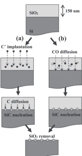
We prepared samples with two kinds of methods of C ion implantation and CO thermal diffusion to synthesize SiC NCs at SiO2/Si interface. These pro- cesses are schematically shown in Fig. 1.
In the former process, we first performed 25 keV C+ ion implantation with a fluence of 2×1016 cm-2 at RT in a thin SiO2 layer with 150 nm thick synthe- sized by dry thermal oxidation of Si(001) substrates at 1000℃ for 3 h under atmospheric pressure. The in- cident energy of 25 keV was chosen to be implanted in the SiO2 layer in the very vicinity of the interface.
The C-implanted samples were then annealed at 1000 and 1100 ℃ for 1 h in Ar ambience to enhance the diffusion of the C atoms to the interface. The depth profile of the implanted C, before and after eliminating the capped SiO2 layer, was analyzed by resonant elastic Rutherford backscattering (RBS) of
12C(p, p)12C at 1.737 MeV using a 1-MV tandem-type Pelletron accelerator 3).
In the latter process, the same SiO2/Si(001) samples were thermally annealed in CO ambience at 1100℃ for 0.5, 1 and 2 h under a pressure of 0.2 bar. In the previous works, SiC NCs are known to be synthesized at the SiO2/Si interface because of CO diffusion through the SiO2 network and chemical reaction with the interfacial Si. Since the nucleation density of SiC nanocrystals depends on the CO pres- sure, we controlled the CO pressure to be 0.2 bar so
that the density of nanocrystals did not become too large 4-8). Surface morphology was observed by atom- ic force microscopy (AFM) and scanning tunneling microscope (STM) after removing the SiO2 layer by HF treatment.
Results
Calibration of incident energy and scattering cross section for 12C(p, p)12C resonance
The detection sensitivity of low atomic number (Z) elements existing in high Z materials is quite poor in the conventional RBS analysis due to low scatter- ing cross section. However, the cross section is reso- nantly enhanced when the summation of incident energy in the center of mass system and nuclear energy generated by the formation of compound nu- cleus corresponds to the exited energy levels of the compound nucleus. The energy conservation rule is written by
Fig. 1. Formation processes of SiC NCs in SiO2/Si samples by C ion implantation (a) and CO thermal dif- fusion methods (b).
where and are the mass of projectile and tar- get atoms, respectively. is the incident energy of projectile in the laboratory system (L-system).
is the energy levels of exited states for compound nucleus. is the energy generated by mass defect in the nuclear compound reaction; defined by
In the present resonance of 12C(p, p)12C, the nuclear reaction equation is given by
and the value is estimated to be 1.9435 MeV.
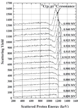
Fig. 2 shows the energy levels of 13N atomic nucle- us3). We can find that the first to third exited states with the nuclear spins and parities of J = 1/2+, 3/2-, and 5/2+ at Eex = 2.365, 3.502, and 3.547 MeV, re- spectively. It is well known that the last state of J = 5/2+ at 3.547 MeV shows significantly narrow reso- nance of 50 keV at 1.737 MeV in the L-system.
We first calibrated the terminal voltage of accel- erator measured by a generating voltmeter (GVM) using the narrow resonance of 12C(p, p)12C at 1.737 MeV. Figure 3 shows the RBS spectra observed for a graphite substrate at a scattering angle of 160° as a function of terminal voltage monitored by GVM from 0.850 to 0.950 MV. In accordance with kine- matic relations in the elastic collision at the surface, the proton energy scattered from the carbon atoms existing on the top surface at a scattering angle of 160°is calculated to be 1.290 MeV for the incident proton beam with the resonant energy of 1.737 MeV.
As can be shown in Fig. 2, the surface resonance is clearly observed at the GVM voltage of 0.92 MV,
suggesting that the proton ions accelerated by that voltage was found to correspond to the resonance energy of 1.737 MeV.
Next, we calibrated the resonant differential cross section at 1.737 MeV by a shallowly C-implanted sample in a Si substrate with an areal density of 4.0
×1016 cm-2. Fig. 4 shows RBS spectrum obtained by
12C(p, p)12C resonance at 1.737 MeV. It is well known that Si has also broad resonance around 1.7 MeV.
A small sharp peak is clearly observed around the energy of 1240 keV, which corresponds to the signal of the 12C(p, p)12C resonance. From the scattering yield, the differential scattering cross section for the resonance at a scattering angle of 160° was estimated to be 8×10-25 cm2 sr-1, which was 50 times higher than that for the ordinary Rutherford scattering. It is suggested that the number of 12C atoms with an order of 1015 cm-2 can be sensitively detected.
Formation of SiC NCs at SiO2/Si interface by C implantation
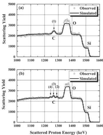
In this section, we show the results of SiC NCs formed by C ion implantation in SiO2/Si followed by annealing 9). Fig. 5 shows resonant RBS spec- tra observed for the samples as-implanted (a) and Fig. 2. Energy levels of 13N atomic nucleus3).
Fig. 3. RBS spectra observed for graphite at various ac- celeration voltages monitored by GVM.
4 Science Journal of Kanagawa University Vol. 30, 2019
post-annealed at 1000℃ (b). According to the scatter- ing yield from 12C atoms observed in Fig. 5(a), the areal density of 12C was estimated to be 2 ×016 cm-2, which is found to be the same as the C fluence. In a RBS spectrum, the energy of scattered projectiles is strongly related to the depth in which the scatter- ing centers are located. The scattered proton energy arrowed in Fig. 5(a) indicates that the implanted C atoms were distributed in the SiO2 layer around the depth of 50 nm measured from the surface. On the other hand, three small peaks were separately observed after annealing at 1000℃ as shown in Fig.
5(b). The peaks located at higher (2) and lower (4) energies correspond to the C atoms diffused to sur- face and interface, respectively. The intermediate peak (3) is attributed to the C atoms in SiO2 layer.
This fact shows that half of implanted C atoms was segregated to the surface and the interface by posta- nealing at 1000℃.
After eliminating the capped SiO2 layer by dip- ping the sample in diluted HF solution, the signal from C was entirely disappeared as shown in Fig. 6.
It shows that the postannealing at 1000℃ enhances the C diffusion to the surface and the interface; how- ever, the sufficient C atoms could not be fixed at the sites by this method.
Formation of SiC NCs at SiO2/Si interface by direct CO annealing
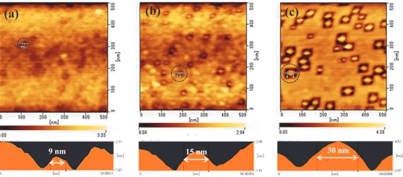
We then investigated the formation of SiC NCs by direct annealing of SiO2/Si specimen in CO gas am- bience. Fig. 7 shows surface protrusion image and cross-sectional shapes of one of NCs for the samples with different annealing time after removing the
SiO2 layer by HF treatment observed by AFM. It is clearly found that epitaxially oriented NCs were formed on the Si(001) surface. The nucleation densi- ty of NCs is found to be about 1.0×1010 cm-2 regard- less of annealing time. This density is sufficiently low necessary for the optical measurement of the individual NCs by STL spectroscopy. The diameter of NCs observed for the samples annealed for 0.5, 1 and 2 h was estimated to be 10, 15 and 30 nm, re- spectively. It is found that the cluster size strongly depends on the annealing time. It should be noted that the quantum size effect becomes remarkable Fig. 4. RBS spectra at the resonance observed for shal-
lowly C-implanted Si (001) substrate with 4×1016 cm-2.
Fig. 6. RBS spectra after eliminating the capped SiO2
layer entirely.
Fig. 5. Resonant RBS spectra observed for the samples as-implanted (a) and post-annealed at 1000℃ (b).
when the size of NCs is 10 nm or less, so that the semiconductor NCs are likely to emit luminescence.
The annealing period of 0.5 h or less should be therefore suitable for the synthesis of NCs for the measurement of STL spectroscopy.
Fig. 8 shows a typical RHEED pattern observed for the samples on which the NCs were formed.
The electron beam with an energy of 20 keV was incident along the [110]-axis. The streak patterns indicated by yellow arrows are attributed to the dif- fraction from the Si(001) surface. In addition, one can see bright spot-like patterns, whose configura- tion was independent of the azimuth direction of incident electron beam. It is suggested that the ob- served pattern is therefore derived to be the diffrac- tion laterally transmitted through 3-dimensional fine structure. The symmetry and distance of the diffraction spots indicated that the NCs are crystal-
line 3C-SiC.
As can be clearly seen in Fig. 7, the NCs of each sample have characteristic shape surrounded by squared pits. These pits are caused by forming SiOx
compound in accordance with the following reaction at the SiO2/Si interface:
2CO + 3Si → 2SiC + SiO2,
after CO diffuses in SiO2 without dissociating and dissociates. The pits are thus formed after removing thermal oxide and SiOx with HF 10).
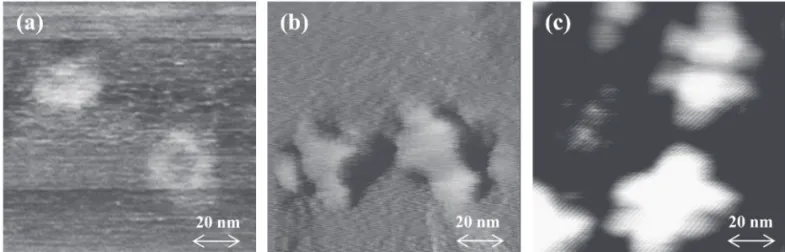
Fig. 9 shows the surface protrusion obtained by STM observation. In order to emerge NCs on the surface for STM measurements, we performed wet chemical preparations by alternately dipping in HNO3 and HF solution several times. In the STM images, we can clearly see SiC NCs with a charac- teristic cross shape, whose size strongly depends on the annealing time. The NCs were found to be co- alesced each other with increasing annealing time.
Discussion
We performed the synthesis of SiC NCs on a crystal- line Si(001) surface with two kinds of procedures of C implantation and CO thermal diffusion into SiO2/Si interface. In the former process, we could not form sufficient SiC NCs at the SiO2/Si(001) interface since the diffusion of C to the interface was not enough promoted by thermal annealing at 1000℃. We also tried higher temperature annealing of 1100℃; however the superficial SiO2 layer was damaged by the annealing process; eventually Formation of SiC NCs at SiO2/Si interface by
direct CO annealing
We then investigated the formation of SiC NCs by direct annealing of SiO2/Si specimen in CO gas ambience. Figure 7 shows surface protrusion image and cross-sectional shapes of one of NCs for the samples with different annealing time after removing the SiO2 layer by HF treatment observed by AFM. It is clearly found that epitaxially oriented NCs were formed on the Si(001) surface. The nucleation density of NCs is found to be about 1.0×1010 cm-2 regardless of annealing time. This density is sufficiently low necessary for the optical measurement of the individual NCs by STL spectroscopy. The diameter
of NCs observed for the samples annealed for 0.5, 1, and 2 h was estimated to be 10, 15, and 30 nm, respectively. It is found that the cluster size strongly depends on the annealing time. It should be noted that the quantum size effect becomes remarkable when the size of NCs is 10 nm or less, so that the semiconductor NCs are likely to emit luminescence. The annealing period of 0.5 h or less should be therefore suitable for the synthesis of NCs for the measurement of STL spectroscopy.
Figure 8 shows a typical RHEED pattern observed for the samples on which the NCs were formed. The electron beam with an energy of 20 keV was incident along the ሾͳͳതͲሿ-axis. The streak patterns indicated by yellow arrows are attributed to the diffraction from the Si(001) surface. In addition, one can see bright spot-like patterns, whose configuration was independent of the azimuth direction of incident electron beam. It is suggested that the observed pattern is therefore derived to be the diffraction laterally transmitted through 3-dimensional fine structure. The symmetry and distance of the diffraction spots indicated that the NCs are crystalline 3C-SiC.
As can be clearly seen in Fig. 7, the NCs of each sample have characteristic shape surrounded by squared pits. These pits are caused by forming SiOx compound in accordance with the following reaction at the SiO2/Si interface:
Fig.7. AFM images and cross-sectional shapes of NC for the samples with different annealing times of 0.5 (a), 1 (b), and 2 h (c).
(a) (b) (c)
9 nm 15 nm 30 nm
Fig.8.RHEED pattern for the NC-formed Si(001) surface.
○○,○○ 他
:○○○○○○○○○○○○○○○○○○○○○○○○○
23Formation of SiC NCs at SiO2/Si interface by direct CO annealing
We then investigated the formation of SiC NCs by direct annealing of SiO2/Si specimen in CO gas ambience. Figure 7 shows surface protrusion image and cross-sectional shapes of one of NCs for the samples with different annealing time after removing the SiO2 layer by HF treatment observed by AFM. It is clearly found that epitaxially oriented NCs were formed on the Si(001) surface. The nucleation density of NCs is found to be about 1.0×1010 cm-2 regardless of annealing time. This density is sufficiently low necessary for the optical measurement of the individual NCs by STL spectroscopy. The diameter
of NCs observed for the samples annealed for 0.5, 1, and 2 h was estimated to be 10, 15, and 30 nm, respectively. It is found that the cluster size strongly depends on the annealing time. It should be noted that the quantum size effect becomes remarkable when the size of NCs is 10 nm or less, so that the semiconductor NCs are likely to emit luminescence. The annealing period of 0.5 h or less should be therefore suitable for the synthesis of NCs for the measurement of STL spectroscopy.
Figure 8 shows a typical RHEED pattern observed for the samples on which the NCs were formed. The electron beam with an energy of 20 keV was incident along the ሾͳͳതͲሿ-axis. The streak patterns indicated by yellow arrows are attributed to the diffraction from the Si(001) surface. In addition, one can see bright spot-like patterns, whose configuration was independent of the azimuth direction of incident electron beam. It is suggested that the observed pattern is therefore derived to be the diffraction laterally transmitted through 3-dimensional fine structure. The symmetry and distance of the diffraction spots indicated that the NCs are crystalline 3C-SiC.
As can be clearly seen in Fig. 7, the NCs of each sample have characteristic shape surrounded by squared pits. These pits are caused by forming SiOx compound in accordance with the following reaction at the SiO2/Si interface:
Fig.7. AFM images and cross-sectional shapes of NC for the samples with different annealing times of 0.5 (a), 1 (b), and 2 h (c).
(a) (b) (c)
9 nm 15 nm 30 nm
Fig.8.RHEED pattern for the NC-formed Si(001) surface.
Fig. 7. AFM images and cross-sectional shapes of NC for the samples with different annealing times of 0.5 (a), 1 (b) and 2 h (c).
Fig. 8. RHEED pattern for the NC-formed Si(001) sur- face.
6 Science Journal of Kanagawa University Vol. 30, 2019
some cracks were formed on the sample. The an- nealing time should be considered carefully.
In the latter process of CO diffusion, we suc- ceeded in the synthesis of SiC NCs within the size of about10 nm by short annealing of 0.5 h. The sizes of the SiC NCs became bigger by annealing for longer period (> 0.5 h), though the number of the NCs was almost constant (1×1010 cm-2). It is suggested that NCs grow randomly on the SiO2/Si interface at the early stage of CO diffusion (< 0.5 h). After a criti- cal time, the nucleation takes place beside already formed NCs. Consequently, the annealing time should be shorter (< 0.5 h) to form small NCs with several nanometers. However, there have been also some discussions that the critical time is existed for beginning the formation of NCs in the previous stud- ies 11). The detailed formation process of NCs should be considered on pressure, temperature, and time in CO annealing process. The optimization of such pa- rameters in annealing is therefore a quite important issue to make SiC NCs with a quantum size.
In summary, we investigated the synthesis of SiC NCs within 10 nm on a crystalline Si(001) sur- face by C implantation and CO diffusion processes aiming at the sample preparation for tunneling luminescence spectroscopy. By annealing the SiO2/ Si sample in 0.2 bar CO ambience at 1000℃ for 0.5 h, NCs in about 10 nm size were formed at the in- terface. RHEED pattern showed that the NCs con- sist of cubic silicon carbide structure. Parameters in annealing such as pressure, temperature, and time should be optimized for further decrement of the NC size for the suitable sample of STL measurements by CT probe.
References
1) Murashita T (1997) Novel conductive transparent tip for low-temperature tunneling-electron luminescence microscopy using tip collection. J. Vac. Sci. Technol.
B 15: 32-37.
2) Omi H, Sychugov I, Kobayashi Y and Murashita T (2009) New microscope combines optical and electri- cal excitation into a single scanning tunneling micro- scope unit for simultaneous characterization of near- field luminescence for individual nanostructures.
Kenbikyo 44: 174-178.
3) Ajzenberg-Selove F (1991) Energy Levels of Light Nuclei A = 13-15. Nuclear Physics A 523: 1-196.
4) Cavellin CD, Trimaille I, Ganem JJ, D’Angelo M, Vickridge I, Prongrácz A and Battistig G (2009) An
18O study of the interaction between carbon monox- ide and dry thermal SiO2 at 1100°C. J. Appl. Phys.
105: 033501/1-7.
5) Pongrácz A, Hoshino Y, D’Angelo M, Cavellin CD, Ganem JJ, Trimaille I, Battistig G, Josepovits KV, and Vickridge I (2009) Isotopic tracing study of the growth of silicon carbide nano-crystals at the SiO2/ Si interface by CO annealing. J. Appl. Phys. 106:
024302/1-5.
6) Deokar, G, D’Angelo M and Deville Cavellin C (2011) Synthesis of 3C-SiC Nanocrystals at the SiO2/Si Interface by CO2 Thermal Treatment. J. Nanosci.
Nanotechnol. 11: 1-5.
7) Pécz B, Makkai Zs, Pongrácz A, Bársony I, Deák P and Battistig G (2007) Formation of epitaxial SiC nanocrystals. Surf. Sci. 601: 2671-2674.
8) Pongrácz A, Battistig G, Dücső Cs, Josepovits KV and Deák P (2007) Structural and electronic proper- ties of Si/SiO2 MOS structures with aligned 3C-SiC nanocrystals in the oxide. Mater. Sci. Eng. C 27:
Fig. 9. Surface protrusion images observed by STM for CO diffused samples at 1100℃ for 0.5 (a), 1.0 (b), and 2.0 h (c).
Acknowledgments
The authors would like to acknowledge Mr. Y. Saito and Dr. T. Murashita for his great supports and valuable comments in this study. This research was partly supported by a grant from the Research In- stitute for Integrated Science, Kanagawa University (RIIS201801).
1444-1447.
9) Voelskow M, Panknin D, Polychroniadis EK, Ferro G, Godinnion P, Mestres N, Skorupa W, Monteil Y and Stoemenos J (2004) Epitaxial SiC formation at the SiO2/Si interface by C+ implantation into SiO2
and subsequent annealing. Mater. Sci. Forum 483- 485: 233-236.
10) Zhang L, Chen LQ and Du Q (2007) Morphology of critical nuclei in solid-state phase transformations.
Phys. Rev. Lett. 98: 265703/1-4.
11) Sugimoto T (2007) Underlying mechanisms in size control of uniform nanoparticles. J. Colloid Interface Sci. 309: 106-118.