INVITED PAPER
Special Section on Josephson Junctions — Past 50 years and Future —NbN-Based Overdamped Josephson Junctions for Quantum Voltage Standards
Hirotake YAMAMORI†a),Nonmember, Takahiro YAMADA†,Member, Hitoshi SASAKI†, andSatoshi KOHJIRO†,Nonmembers
SUMMARY 524,288 NbN-based Josephson junctions were integrated to produce a programmable Josephson voltage standard (PJVS) on a die of 15 mm×15 mm, and the PJVS circuit was cooled to 10 K using a cryo- cooler and operated with a current margin of about 1.0 mA. Although an output voltage of 10 V was required for a voltage standard, the circuit was designed to generate the maximum output voltage of 17 V because it was difficult to avoid a reduction of the output voltage due to defects. Although a perfect chip without any defect was rarely fabricated, the high voltage chip that generated at least 10 V was fabricated with the fabrication yield of larger than 30%. The fabrication yield was also improved by optimizing the film growth conditions to reduce the film stress and the number of par- ticles. Applications for a secondary voltage standard and an ac Josephson voltage standard are also described.
key words: NbN, TiN, SNS, voltage standard, cryocooler
1. Introduction
NbN is a promising material for high-frequency radiation detectors such as low-noise terahertz SIS mixers because it has large gap frequencies of up to 1.4 THz [1], [2]. NbN/Nb oxide/NbN [3], [4] and NbN/MgO/NbN [5] tunnel junc- tions have been demonstrated for LSI logic circuits. These NbN-based tunnel junctions tend to have relatively high leakage currents, whereas an NbN/AlN/NbN tunnel junc- tion has been demonstrated that has a small leakage current and a high current density for SIS mixer applications [8], [9]. In addition, NbN has a relatively high transition tem- peratureTc, and it is preferable for a phonon-cooled hot- electron bolometer (HEB) superconducting mixer because the IF bandwidth depends on the electron-phonon interac- tion time, which is temperature dependent [6], [7]. NbN is also promising for voltage standard circuits because it has a high operating temperature, which significantly reduces the size and cost of cryocoolers required to cool the cir- cuits. Hamilton et al. demonstrated a programmable Joseph- son voltage standard (PJVS) with a binary divided Joseph- son junction (JJ) array using resistor-shunted Nb/AlOx/Nb junctions [10].
An overdamped junction with non-hystereticI–Vchar- acteristics is necessary for D/A conversion; superconductor- normal metal- superconductor (SNS) JJs are preferable to tunnel junctions with external shunt resistors because SNS
Manuscript received July 4, 2011.
Manuscript revised October 18, 2011.
†The authors are with the National Institute of Advanced In- dustrial Science and Technology (AIST), Tsukuba-shi, 305-8568 Japan.
a) E-mail: [email protected] DOI: 10.1587/transele.E95.C.329
JJs have small floating inductances and high critical current densities of over 50 kA/cm2 that provide a large operating current margin [11]. PJVS circuits have also been demon- strated with overdamped Nb/AlOx/Nb/AlOx/Nb(SINIS) [12] and Nb/Al-AlOx/Nb (SNIS) [13] junctions. Various normal metals (e.g., PdAu [11], MoSi [14], NbSi [15] and HfTi [16]) have been proposed for Nb-based SNS junctions, whereas metal nitrides (e.g., TiN [17] and TaN [18]) have been proposed for NbN-based junctions. While PJVS cir- cuits with output voltages of over 10 V have been demon- strated with Nb/AlOx/Nb/AlOx/Nb [19], Nb/NbSi/Nb [20]
junctions, it is challenges to fabricate such large circuits containing larger than 100,000 JJs with a practical fabrica- tion yield. We have demonstrated a 10-V PJVS circuit using double-stacked NbN/TiN/NbN JJs with a practical fabrica- tion yield of larger than 30% [21].
This paper describes the fabrication and characteristics of an NbN film, an NbN-based overdamped junction, and a JJ array for a voltage standard circuit. It also presents efforts to improve the fabrication yield and the operating current margin. In addition, current under-developed metrological applications are mentioned.
2. NbN-Based Overdamped Josephson Junction
2.1 NbN Film Preparation
Polycrystalline NbN films rather than epitaxial NbN films were used for Josephson voltage standard circuits because many JJs need to be integrated in a relatively large chip area (e.g., 15 mm ×15 mm) and fabrication process for epitax- ial NbN films using a 3-inch-diameter wafer has not been established at the AIST.
The NbN films were deposited on a 3-inch diameter Si wafer by reactive rf-magnetron sputtering using a 6-inch- diameter niobium target in an N2, Ar, and C2H2 gas mix- ture at ambient temperature without intentional heating. The NbN films were deposited using a total pressure of 2 Pa, an Ar gas flow rate of 52 standard cubic centimeters per minute (sccm), an N2 gas flow rate of 2.7 sccm, and an incident power of 600 W, which gave a deposition rate of 1.3 nm/s.
We confirmed the long-term process stability over more than 10 years since NbN films with a critical temperature of about 16 K could be reproducibly prepared at the same N2 flow rate and the same total gas pressure.
The stress in the deposited films was evaluated by esti- Copyright c2012 The Institute of Electronics, Information and Communication Engineers
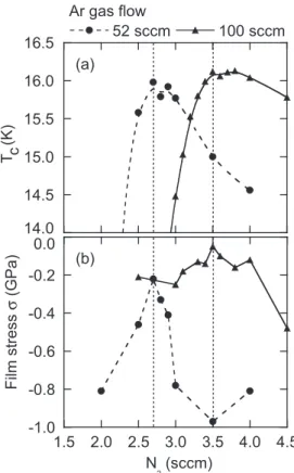
Fig. 1 Dependence ofTcandσon the N2gas flow rate for various Ar gas flow rates.
mating wafer bending using Stoney’s equation [22]. In reac- tive NbN sputtering, the N2partial pressure determines the critical temperature and the Ar partial pressure mainly influ- ences the intrinsic stress [23], [24]. Films with a highTcpre- pared with a low Ar pressure tend to have high film stresses [25]. An NbN film with a highTcand a low film stress is preferable for large-scale integrated circuits because a high film stress may reduce the fabrication yield due to delamina- tion of the film. Figure 1 shows the N2flow rate dependence of the critical temperatureTcand the film stressσsputter de- posited using different Ar flow rates. The film thicknesses are about 200 nm. This result suggests that using higher Ar gas flow rate reduces the film stress. It is also found that the N2 flow rate that maximizeTcand that minimize the film stress are equal, as shown by the broken lines in Fig. 1. As a result, a nearly stress-free NbN film withTc=16 K and ρ20 K=152.3μΩ·cm was obtained at a total sputtering pres- sure of 2 Pa with an Ar gas flow rate of 100 sccm.
2.2 NbN/TiN/NbN Junction
The junctions have an optimum operating frequency Ω(= f/IcRnKj)≈1, whereKj=483 597.9 GHz/V, and the great- est tolerance of the step position to critical current varia- tion in arrays is also obtained atΩ≈1. Consequently, the productIcRn of the junction has to be carefully adjusted by varying the TiN film thickness. Figures 2(a) and (b) respec- tively show the dependences of the critical current Ic and
Fig. 2 Dependence of critical current and junction resistance of NbN/TiN/NbN JJ at 10 K on TiN thickness.
the normal resistanceRnmeasured at 10 K on the TiN thick- nessd. The normal coherent lengthξn is estimated to be about 3.7 nm from the slope in Fig. 2(a) and the equation of Ic ∝ exp(−d/ξn). The TiN film was deposited by reac- tive rf-magnetron sputtering using a titanium target in an N2 gas at the total pressure of 1.33 Pa with the incident power of 600 W. During deposition of the TiN film, the substrate holder was rotated at 10 rpm to improve the uniformity. The TiN film was deposited at a rate of typically 0.02 nm/s. The TiN film had a resistivity ρf of 733μΩ·cm at 4.2 K, and it varied little in the temperature range of 4 to 300 K. The TiN film may be N rich relative to the stoichiometric composi- tion, and it was dark brown and had a transition tempera- ture of 2.7 K. The resistivity of the TiN film was strongly dependent on the total N2 pressure and the N2 flow rate in an Ar and N2 gas mixture. In contrast, the normal junc- tion resistanceRnwas approximately constant; specifically, the normal resistance of the NbN/TiN/NbN junctionRndid not depend on the resistivity of the TiN film. The resistiv- ityρjis estimated to be approximately 318μΩ·cm from the slope in Fig. 2(b) and the equation ofRn =(ρj/L2)d, where L = 2.8μm is the junction size; this resistivity is much smaller than that of the TiN filmρf measured by the four- probe method. The reason for this discrepancy in the re- sistivities is unclear; the films were grown on different sub- strates with different top passivation layers, which may af-
fect the resistivity. Another possible cause is columnar grain growth. Electron scattering from grain boundaries generally dominates the in-plane resistivity, whereas there are no grain boundaries for the vertical resistivity [26].
3. Voltage Standard Circuit
3.1 Design and Fabrication
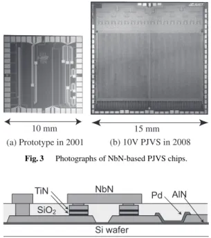
The National Institute of Advanced Industrial Science and Technology (AIST) and the National Institute of Standards and Technology (NIST) jointly demonstrated a D/A conver- sion using 4,096 NbN/TiN/NbN JJs and a 10-V PJVS circuit with 327,680 JJs [21]. Figure 3(a) shows the first proto- type of the PJVS chip and Fig. 3(b) shows the latest PJVS chip that contains 524,288 JJs. The PJVS chip consists of co-planar waveguides (CPWs), JJ arrays, low-pass filters, dc-block capacitors, microwave termination resistors, and a microwave power divider. They were numerically optimized by an electromagnetic simulator.
Figure 4 shows a cross-sectional view of the PJVS cir- cuit and Table 1 lists its specifications. In the chip, the junc- tion arrays were divided into 64 parallel arrays each con- taining 4096 double-junction stacks (8192 JJs). A 16 GHz quarter-wavelength CPW with a specific impedance of 36Ω was connected to two 50ΩCPWs, which functioned as two- way splitters. Six consecutive stages of the two-way splitters were connected in series to divide the microwave into 64 ar- rays. Sixteen cells containing four arrays generate about 1 V each; two of them have binary subarrays with resolutions of 9 bits. The 10 cells having the higher operating current mar- gins were selected from 16 cells to generate a maximum voltage of 10 V; namely, it functions as a decimal DAC and one of the 10 cells with the binary subarrays functions as a 1 V binary DAC to give a high resolution.
The fabrication process for the NbN-based cir- cuit [21] was almost compatible with that for the Nb- based circuit. An AlN film (as an etch stop) and an NbN/TiN/NbN/TiN/NbN multilayer were consecutively de- posited by reactive rf-magnetron sputtering on a 3-inch- dameter Si wafer. The TiN barrier was typically thick 24 nm; this thickness was chosen to provide anIcRnof 33μV at 10 K. The NbN counter electrode, two TiN barriers, and an NbN middle electrode were patterned to define Josephson junctions by reactive ion etching (RIE), and the base elec- trode was subsequently patterned by RIE. The photoresist was removed using an N-methyl-2-pyrrolidone (NMP) jet, which was 0.1 mm in diameter and had a pressure of 8 MPa.
To fabricate the termination resistors, a Pd film was sputter deposited and then patterned by the lift-offmethod. A 400- nm-thick SiO2film as the electrical isolation was deposited by rf sputtering. Via holes were formed by RIE of the SiO2
layer and a portion of the counter electrodes. A 600-nm- thick NbN film was deposited as a wiring layer. However, because of the previously patterned structures, this NbN film was not flat and had grain boundaries at the step edges. To prevent a significant reduction in the wiring critical current,
Fig. 3 Photographs of NbN-based PJVS chips.
Fig. 4 Cross-sectional view of PJVS circuit with a double barrier JJ.
Table 1 Specifications.
Chip size 15.28 mm×14.70 mm
Number of JJs 524 288
Number of JJs/stack 2 (double barrier) Junction size 3.4μm square (design)
2.8μm square (measured) Electrode material polycrystalline NbN Normal metal material TiN
Minimum line and space 1.6μm Critical current density 70 kA/cm2 Junction resistance 6.0 mΩ Maximum output voltage 17 V @ 16.0 GHz
20 V @ 18.5 GHz Operating temperature 10 K
the surface of the NbN wiring was planarized by chemical- mechanical polishing (CMP). An additional NbN film was deposited on the flat surface and these films were patterned by RIE. Finally, a SiO2passivation layer was deposited and contact holes were formed to the dc bias pad by RIE.
3.2 Fabrication Yield
There is generally a trade-off between the microwave fre- quency of the JJ array and the number of junctions to ob- tain a constant voltage. Since the microwave frequency was 16 GHz, the cost of the microwave source, cables and other components was relatively low. The constant volt- age step was relatively small. At this frequency, more than 300,000 JJs are required to generate an output voltage of 10 V, whereas only 70,000 junctions are needed to gener- ated the same output voltage at a frequency of 90 GHz [19].
A large chip area is required to integrate so many junctions, which could significantly reduce the fabrication yield. One way to overcome this problem is to vertically stack JJs; for example, more than 300,000 JJs can be integrated on a sin-
gle die of about 200 mm2 using double- or triple-stacked junctions [20], [21].
There were major and minor defects for the PJVS cir- cuit. A short circuit between the array and the ground and an open or resistive junction across the array are critical defects because they affect a total voltage of the array. On the other hand, missing junctions due to a superconducting bridge be- tween electrodes or a pin hole in the barrier are admissible because it does not generate any voltage. Defects can also damage microwave circuits and reduce the operating current margin. We primarily attempted to reduce the probability of critical defects to fabricate as many available die as possi- ble. A microscopy observation suggested that both short and open circuits are formed by delamination of the insulating layer due to particles, film stress, or contamination. To re- move particles and contamination from the wafer, an NMP jet was used to remove the photoresist after patterning by RIE. In addition, the air conditioner in the clean room was upgraded to maintain the relative humidity at about 50%, and eventually water marks due to a dew condensation were prevented from forming on the wafer surface.
We have used an MgO as etch stop layers for many years, but we have neglected to consider that the etch stop layer also contains particles that reduce the fabrication yield.
We found that Al or AlN layers contained smaller particles than MgO layers and that the particle density depended on the film deposition conditions (e.g., pressure and incident rf-power). Figure 5 shows the dependences of the particle density in the AlN film and the film thickness on the inci- dent rf power for film deposition. The films were deposited for 300 s; the film thickness was approximately proportional to the rf power. The number of particles in the film was esti- mated by counting the number of particles in a certain area of a microscopy image; this method was precise enough for qualitative estimation. Fewer particles were formed when the AlN film was sputter deposited at higher incident rf pow- ers and for shorter deposition times.
In addition, we experimentally confirmed that the ef-
Fig. 5 Dependence of particle density in an AlN film on incident rf power during film deposition.
fective fabrication yield was significantly improved by using a PJVS chip with additional JJs. Although an output voltage of 10 V was required for a voltage standard, the circuit was designed to generate the maximum output voltage of 17 V.
The junction array is divided into 16 cells, and dc-bias cur- rents will not be supplied to the cells including minor defects such as a missing junction so that they constantly generate zero volt. Although a perfect chip without any defect was fabricated with the fabrication yield of a few percent, the high voltage chip that generated at least 10 V was fabricated with that of larger than 30%.
3.3 Operating Current Margin
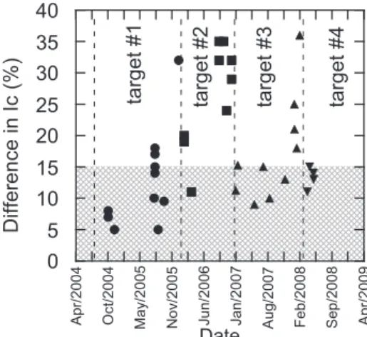
Since the operating current margin of the PJVS is deter- mined by both the zeroth (n =0) and firstn = 1 constant voltage steps and since the n = 0 step is typically much larger than then=1 step, we discuss the operating current margin in terms of the n = 1 step. The double-barrier JJ reduced the chip area and increased the number of dies on a wafer, which lowered the cost and increased the fabrication yield. Figure 6 shows a plot of the secular change in the difference between theIcof the upper and lower junctions over about 5 years. It suggests that this difference is smaller than 15% up to about 1 year after exchanging the Nb target and it exceeds 30% after about 1 year. Therefore, we ex- changed the Nb target after 100 elapsed hours even if the Nb target was still thicker than half of the Nb target. Figure 7 shows the relation between the normalizedn = 1 Shapiro step height and the difference inIcfor the upper and lower junctionsΔIc; it was numerically calculated using the resis- tively shunted junction (RSJ) model [27]. For simplicity, the variation inRnwas not taken into account. A difference in Icof 15%, which is experimentally observed in typical double-barrier junctions, suppressed the current margin by about 20%, while a difference inIcof 40% suppressed the margin by about a factor of two. These results suggest that a difference inIcfor the upper and lower junctions of about 15% does not critically affect the practical operating current
Fig. 6 5-year secular change in the difference inIcfor the double-barrier junctions sputter deposited using different Nb targets.
Fig. 7 Numerically calculatedn=1 Shapiro step height as a function of the difference inIcbetween the upper and lower junctions.
Fig. 8 Dependence of then=1 step height on the number of JJs. Closed circles and triangles show measured step heights and closed and broken lines indicate numerical calculation results using the RSJ model for differ- ent variations inIc.
margin.
The applied microwave power decreased rapidly in the dissipative junction array. The microwave power at the end of the arrayPendis given by Pend ∝exp(−RnN/Z0), where Rn is the junction resistance, N is the number of JJs, and Z0 is the characteristic impedance of the array. Then = 1 Shapiro step heightIs1 is expressed by the Bessel function J1(vend) as a function of the microwave voltagevend when biased with a current source. When the microwave voltage vendis sufficiently small to use the approximationJ1(vend)∝ vend, then=1 Shapiro step heightIs1can be approximated by
Is1∝exp
−Rn 2Z0
N
(1) This is a simple qualitative approximation. For a quanti- tative investigation, a numerical simulation using the RSJ model was performed. Figure 8 shows the dependence of the n=1 step height on the number of JJs. The solid and bro-
Fig. 9 Dependence of the operating current margin for the 8192 JJs array on the temperature and microwave power.
ken lines indicate step heights numerically calculated using the RSJ model for different variations in Ic, and the closed circles and triangles show the experimentally measured val- ues. Since the variation inRnwas not taken into account in the calculation, the calculated step heights were larger than the measured ones. The effect of the Josephson penetration depth was not taken into account, which could account for the discrepancy between the measured and calculated values for smallNand largeIs1.
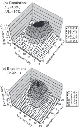
Figure 9(a) shows the numerically calculated depen- dence of then = 1 Shapiro step height on the microwave current and temperature for 4096 double-stacked junctions (=8192 JJs). The microwave bias applied to the junctions had a frequency of 16 GHz. Ic andRn for the upper and lower junctions were assumed to differ by 10%. In this cal- culation, measured values for the temperature dependences of IcandRn were used, while the temperature dependence ofRnin the temperature range of 7 to 13 K was sufficiently small forRnto be approximated by a constant value of 6 mΩ.
Figure 9(b) shows the measured dependence of then = 1 Shapiro step height on the microwave current and temper- ature for 4096 double-stacked junctions (=8192 JJs). For both the calculations and the measurements, the maximum step heights were obtained at a temperature of about 10 K for which the productIcRnwas 33μV; these maximum step heights were approximately equal.
Figure 10 shows the current-voltage (I–V) character- istics of 16 array cells in a 10 bit 1 V PJVS circuit that has double-junction stack arrays. TheI–Vs characteristics
Fig. 10 Current-voltage characteristics of binary divided double-barrier JJ arrays containing 64, 64, 128, 256, 512, 1024, 2048, 4096, and 8192
×7 JJs measured with no microwave bias at 10.5 K. The difference inIc
(δIc=50%) due to the magnetic flux trap is much larger than that (ΔIc= 16%) between the upper and lower JJs.
Fig. 11 Current-voltage characteristics of perfect chip with 524,288 NbN/TiN/NbN junctions irradiated by 16 GHz microwaves at 9.79 K. All 16 cells were biased with the same dc currents and the common step height to all cells was about 1.0 mA (see inset).
were measured without a microwave bias at a temperature of 10.5 K, which was obtained by cooling with a cryocooler.
There are 64, 64, 128, 256, 512, 1024, 2048, 4096, and 8192
×7 junctions in each cell. A magnetic flux trapδIccauses a 50% variation inIc, which is much larger than the 16%
variation between the upper and lower junctionsΔIc. We at- tempted to eliminate the magnetic flux by heating the chip aboveTc, but it was not possible to remove all the magnetic flux. The variation inIcdue to magnetic flux is currently the most critical bottleneck for improving the operating current margin.
Figure 11 shows typical current voltage characteristics of a perfect chip that has 524,288 NbN/TiN/NbN junctions irradiated by 16 GHz microwave at 9.79 K. The inset shows that the flat step was about 1 mA, which was about five times higher than that generated by a conventional Josephson volt- age standard. The total voltage was 17 V, and it was con- firmed that there was no missing junction because the mea- sured voltages generated by all 16 cells containing 32,768
JJs each agreed with the theoretical ones within the gain er- ror of the voltmeter in a smaller voltage range [28].
4. Current Challenges
4.1 Compact Josephson Voltage Standards
Figure 12(a) shows a 10-V PJVS system that was cooled by a cryocooler rather than liquid helium. Josephson volt- age standard systems are used as primary voltage standards at national metrology institutes and Zener voltage standards are used as secondary voltage standards. However, a low- cost and transportable PJVS system would be more suitable for secondary voltage standards at laboratories and facto- ries. NbN-based JJ can reduce the volume and cost of PJVS system since they can use a more compact cryocooler due to their high critical temperature (see Fig. 12). The chip for the PJVS has a high power consumption (≈100 mW) and the binary array requires many wires for the dc bias current, resulting in a high heat flow (≈300 mW) from room tem- perature. An increase in the operating temperature of 1 K reduces the required cooling power by about 200 mW al- though it depends on the cryocooler and compressor used.
Therefore, to realize a rack-mountable system it is neces- sary to increase the operating temperature and to reduce the output voltage.
Figure 12(b) shows a rack-mountable PJVS system that is currently being developed as a secondary standard. Ex- cept for the He gas compressor, all the components are en- closed in a chassis with dimensions 430(W) ×250(H) × 500(D) mm (19 inch 6U case). A 2-V PJVS chip rather than a 10-V PJVS chip is chosen to reduce the heat generated in the chip and an output voltage of 20 V is generated using a voltage-multiplier circuit at room temperature [29]. The intrinsic accuracy of the PJVS will be degraded by the use of semiconductor circuits, but it is sufficiently accurate as a secondary voltage standard. Since there is no secular change in the Josephson voltage standard, the period between cali- brations will be reduced, which represents a significant ad- vantage of using Josephson voltage standards as secondary voltage standards.
4.2 Ac Josephson Voltage Standards
The ac-dc transfer standard is one of the basic electrical standards by which the ac voltage and ac current are de- duced from their dc counterparts for frequencies in the range 10 Hz to 1 MHz. Although dc voltage standards are estab- lished using a Josephson voltage standard, ac voltage stan- dards are still derived from the dc voltage standard by com- paring the electric power between ac and dc voltages by converting the power to heat. Therefore, direct synthesis of an ac (sine) waveform by using a high-precision D/A con- verter is being attempted. The Josephson arbitrary wave- form synthesizer (JAWS) proposed by the NIST is one of the most promising techniques for covering a high-frequency range from kilohertz to megahertz. Benz et al. achieved
Fig. 12 (a) 10-V PJVS system for use as a primary standard. (b) Rack- mountable PJVS system that is currently being developed as a secondary standard. It has dimensions 430(W)×250(H)×500(D) mm (19-inch 6U case).
a record rms voltage of 275 mV using Nb-based JJs; they aim to eventually fabricate a 1 V system [30]. Maruyama et al. generated bipolar sinusoidal voltage waveforms at a fre- quency of 16 kHz with a peak-to-peak amplitude of 36.1 mV (which corresponds to an rms voltage of 12.7 mV) using 1600 NbN/TiN/NbN JJs [31]. For successful operation of JAWS with wide margins and high output voltages, many uniform JJs have to be integrated into an array. Meander ar- rays [16], tapered arrays [32], and self-phase-locked arrays [33] have been proposed. The next-generation ac voltage standard based on the Josephson effect is important and in- teresting not only for metrological studies but also from a physics perspective (e.g., redefining the Boltzmann’s con- stant [34]).
5. Conclusion
A 10-V PJVS using double-stacked NbN/TiN/NbN JJs was successfully demonstrated at 10 K cooled with a cryocooler.
The fabrication yield for the chip containing 524,288 JJs was improved by optimizing the film growth conditions, and a design delivering the higher output voltage of 17 V also contributed to increase the number of available chips for the 10-V PJVS. The NbN-based PJVS operating at 10 K with a compact cryocooler was significantly smaller and cheaper than conventional systems, which makes it promising for
use as a secondary voltage standard in laboratories and fac- tories. We are continuing to reduce its size and cost. In ad- dition, an arbitrary waveform synthesizer is currently being developed as a quantum ac voltage standard for metrological and industrial applications.
Acknowledgement
We thank P.D. Dresselhaus and S.P. Benz for their par- ticipation in a joint project on developing of 10-V pro- grammable Josephson voltage standards. We also thank A. Shoji, H. Yoshida, and Y. Nakamura for their support and encouragement.
References
[1] Y. Uzawa, Z. Wang, and A. Kawakami, “Terahertz NbN/AlN/NbN mixers with Al/SiO/NbN microstrip tuning circuits,” Appl. Phys.
Lett., vol.78, pp.680–682, 1998.
[2] A. Kawakami, Y. Uzawa, and Z. Wang, “Development of epitaxial NbN/MgO/NbN- superconductor- insulator- superconductor mixers for operations over the Nb gap frequency,” Appl. Phys. Lett., vol.83, pp.3954–3956, 2003.
[3] S. Kosaka, A. Shoji, M. Aoyagi, F. Shinoki, H. Nakagawa, S.
Takada, and H. Hayakawa, “High speed logic operations of all re- fractory Josephson integrated circuits,” Appl. Phys. Lett., vol.43, pp.213–215, 1983.
[4] S. Kosaka, A. Shoji, M. Aoyagi, F. Shinoki, S. Tahara, H. Ohigashi, H. Nakagawa, S. Takada, and H. Hayakawa, “An integration of all refractory Josephson logic LSI circuit,” IEEE Trans. Magn., vol.21, no.2, pp.102–109, 1985.
[5] A. Shoji, M. Aoyagi, S. Kosaka, F. Shinoki, and H. Hayakawa, “Nio- bium nitride Josephson tunnel junctions with magnesium oxide bar- riers,” Appl. Phys. Lett., vol.46, pp.1098–1100, 1985.
[6] G.N. Gol’tsman, A.D. Semenov, Y.P. Gousev, M.A. Zorin, I.G.
Gogidze, E.M. Gershenzon, P.T. Lang, W.J. Knott, and K.F. Renk,
“Sensitive picosecond NbN detector for radiation from millime- ter wavelength to visible light,” Supercond. Sci. Technol., vol.4, pp.453–456, 1991.
[7] B.S. Karasik, W.R. McGrath, and R.A. Wyss, “Optimal choice of material for HEB superconducting mixers,” IEEE Trans. Appl. Su- percond., vol.9, no.2, pp.4123–4216, 1999.
[8] Z. Wang, A. Kawakami, Y. Uzawa, and B. Komiyama, “High crit- ical current density NbN/AlN/NbN tunnel junctions fabricated on ambient temperature MgO substrates,” Appl. Phys. Lett., vol.64, pp.2034–2036, 1994.
[9] Z. Wang, Y. Uzawa, and A. Kawakami, “NbN/AlN/NbN tunnel junctions applied as terahertz SIS mixers,” IEICE Trans. Electron., vol.E80-C, no.10, pp.1258–1264, Oct. 1997.
[10] C.A. Hamilton, C.J. Burroughs, and R.L. Kautz, “Josephson D/A converter with fundamental accuracy,” IEEE Trans. Instrum. Meas., vol.44, no.2, pp.223–225, 1995.
[11] S.P. Benz, “Superconductor- normal- superconductor junctions for programmable voltage standard,” Appl. Phys. Lett., vol.67, pp.2714–2716, 1995.
[12] H. Schulze, F. M¨uller, R. Behr, J. Kohlmann, J. Niemeyer, and D.
Balashov, “SINIS Josephson junctions for programmable Joseph- son voltage standard circuits,” IEEE Trans. Appl. Supercond., vol.9, no.2, pp.4241–4244, 1999.
[13] V. Lacquaniti, N.D. Leo, M. Fretto, A. Sosso, F. M¨uller, and J.
Kohlmann, “1 V programmable voltage standards based on SNIS Josephson junction series arrays,” Supercond. Sci. Technol., vol.24, 045004, 2011.
[14] Y. Chong, P.D. Dresselhaus, S.P. Benz, and J.E. Bonevich, “Ef- fects of interlayer electrode thickness in Nb/(MoSi2/Nb)N stacked
Josephson junctions,” Appl. Phys. Lett., vol.82, pp.2467–2469, 2003.
[15] B. Baek, P.D. Dresselhaus, and S.P. Benz, “Co-sputtered amorphous NbxSi1−x barriers for Josephson-junction circuits,” IEEE Trans.
Appl. Supercond., vol.16, no.4, pp.1966–1970, 2006.
[16] O.F. Kieler, J. Kohlmann, and F. M¨uller, “Improved design of su- perconductor/normal conductor/superconductor Josephson junction series arrays for an ac Josephson voltage standard,” Supercond. Sci.
Technol., vol.20, pp.S318–S322, 2007.
[17] Q. Wang, T. Kikuchi, S. Kohjiro, and A. Shoji, “Preparation of NbCxN1−x Josephson junctions with TiNxbarriers,” IEEE Trans.
Appl. Supercond., vol.7, no.2, pp.2801–2804, 1997.
[18] A.B. Kaul, S.R. Whiteley, T. Van Duzer, L. Yu, N. Newman, and J.M. Rowell, “Internally shunted sputtered NbN Josephson junctions with a TaNx barrier for nonlatching logic applications,” Appl. Phys.
Lett., vol.78, pp.99–101, 2001.
[19] H. Schulze, R. Behr, J. Kohlmann, F. M¨uller, and J. Niemeyer,
“Design and fabrication of 10 V SINIS Josephson arrays for pro- grammable voltage standards,” Supercond. Sci. Technol., vol.13, pp.1293–1295, 2000.
[20] P.D. Dresselhaus, M.M. Elsbury, D. Olaya, C.J. Burroughs, and S.P. Benz, “10 volt programmable Josephson voltage standard cir- cuits using NbSi-barrier junctions,” IEEE Trans. Appl. Supercond., vol.21, no.3, pp.693–696, 2011.
[21] H. Yamamori, M. Ishizaki, A. Shoji, P.D. Dresselhaus, and S.P.
Benz, “10 V programmable Josephson voltage standard circuits using NbN/TiNx/NbN/TiNx/NbN double-junction stacks,” Appl.
Phys. Lett., vol.88, 042503, 2006.
[22] G.C. Stoney, “The tension of metallic films deposited by electroly- sis,” Proc. R. Soc. Lond. A, vol.82, pp.172–175, 1909.
[23] Z. Wang, A. Kawakami, Y. Uzawa, and B. Komiyama, “Supercon- ducting properties and crystal structures of single-crystal niobium nitride thin films deposited at ambient substrate temperature,” J.
Appl. Phys., vol.79, pp.7837–7842, 1996.
[24] N.N. Iosad, T.M. Klapwijk, S.N. Polyakov, V.V. Roddatis, E.K.
Kov’ev, and P.N. Dmitriev, “Properties of DC magnetron sputtered Nb and NbN films for different source conditions,” IEEE Trans.
Appl. Supercond., vol.9, no.2, pp.1720–1723, 1999.
[25] S. Kiryu, A. Shoji, S. Kohjiro, and S. Kodaira, “Stress in NbCxN1−x films prepared by reactive Rf magnetron sputtering,” Jpn. J. Appl.
Phys., vol.32, pp.L834–L836, 1993.
[26] S. Kohjiro, A. Shoji, and S. Kiryu, “Magnetic penetration depth and normal-state resistivities of epitaxial and polycrystalline NbCxN1−x
films,” Jpn. J. Appl. Phys., vol.31, pp.L239–L241, 1992.
[27] W.C. Stewart, “Current-voltage characteristics of Josephson junc- tions,” Appl. Phys. Lett., vol.12, pp.277–280, 1968.
[28] T. Yamada, C. Urano, H. Nishinaka, Y. Murayama, A. Iwasa, H.
Yamamori, H. Sasaki, A. Shoji, and Y. Nakamura, “Single-chip 10- V programmable Josephson voltage standard system based on a re- frigerator and its precision evaluation,” IEEE Trans. Appl. Super- cond., vol.20, no.1, pp.21–25, 2010.
[29] H. Sasaki, H. Yamamori, T. Yamada, and A. Shoji, “High-precision voltage multiplier circuit for programmable Josephson voltage stan- dards,” 12th International Superconductive Electronics Conference (ISEC’09), HF-P10, June Fukuoka, Japan, 2009.
[30] S.P. Benz, P.D. Dresselhaus, A. R¨ufenacht, N.F. Bergren, J.R.
Kinard, and R.P. Landim, “Progress toward a 1 V pulse-driven AC Josephson voltage standard,” IEEE Trans. Instrum. Meas., vol.58, no.4, pp.838–843, 2009.
[31] M. Maruyama, C. Urano, N. Kaneko, H. Yamamori, A. Shoji, M.
Maezawa, Y. Hashimoto, H. Suzuki, S. Nagasawa, T. Satoh, M.
Hidaka, and S. Kiryu, “Utilization of a Cryo-prober system for op- eration of a pulse-driven Josephson junction array,” J. Phys.: Conf.
Series, vol.234, p.042020, 2010.
[32] P.D. Dresselhaus, M.M. Elsbury, and S.P. Benz, “Tapered transmis- sion lines with dissipative junctions,” IEEE Trans. Appl. Supercond., vol.19, no.3, pp.993–998, 2009.
[33] H. Yamamori, C. Urano, M. Maruyama, H. Sasaki, and S. Kohjiro,
“Large constant voltage generated with a single array including 65 536 Nb/TiN/Nb Josephson junctions,” Supercond. Sci. Technol., vol.23, 075011, 2010.
[34] S.P. Benz, J. Qu, H. Rogalla, D.R. White, P.D. Dresselhaus, W.L.
Tew, and S.W. Nam, “Improvements in the NIST Johnson noise thermometry system,” IEEE Trans. Instrum. Meas., vol.58, no.4, pp.884–890, 2009.
Hirotake Yamamori was born in Toyama, Japan, in 1968. He received the B.E., M.E., and Ph.D. degrees from Nagoya University, Nagoya, Japan, in 1991, 1993, and 1996, respectively.
In 1996, he joined the Electrotechnical Labo- ratory (ETL), presently the National Institute of Advanced Industrial Science and Technology (AIST), Tsukuba, Japan. From 2003 to 2004, he was with the National Institute of Standards and Technology (NIST), Boulder, CO, as a guest re- searcher.
Takahiro Yamada received the B.E., M.E., and Ph.D. degrees in quantum engineering from Nagoya University, Nagoya, Japan, in 2000, 2002, and 2006, respectively. He was engaged in the research of single-flux-quantum circuits.
In 2006, he joined the National Institute of Advanced Industrial Science and Technology (AIST). His current research interests include a programmable Josephson voltage standard. He is a member of the Japan Society of Applied Physics.
Hitoshi Sasaki was born in Hokkaido, Japan in 1954. He received the M.S. degree in Physics from the Hokkaido University, and Ph.D. de- gree in Engineering from Nagoya University.
In 1979, He joined the Electrotechnical Lab- oratory (ETL), presently the National Institute of Advanced Industrial Science and Technology (AIST), where he has been working on precision electrical measurements. Dr. Sasaki is a member of the Japan Society of Applied Physics and the Institute of Electrical Engineers of Japan.
Satoshi Kohjiro received the B.E., M.E., and Ph.D. degrees from Kyushu University, Fukuoka, Japan, in 1984, 1986, and 1989, re- spectively. In 1989, he joined Electrotechni- cal Laboratory, presently the National Institute of Advanced Industrial Science and Technology.
His specialty is superconducting mixers, oscilla- tors, and SQUIDs. He is a member of the Japan Society of Applied Physics.