SUMMARY Superconducting Transition edge sensor (TES) coupled with a heavy metal absorber is a promising microcalorimeter for Gamma- ray (γ-ray) spectroscopy with ultra-high energy resolution and high detec- tion efficiency. It is very useful for the non-destructed inspection of the nu- clide materials. High resolving power ofγ-ray peaks can precisely identify multiple nuclides such as Plutonium (Pu) and Actinides with high efficiency and safety. For this purpose, we have developed the TES coupled with a tin absorber. We suggest the new device structure using the gold bump post which connects a tin absorber to the thermometer of the superconducting Ir/Au bilayer. High thermal conductivity of the gold bump post realized strong thermal coupling between the thermometer and theγ-ray absorber, and it brought the benefit of large pulse height and fast decay time. Our TES achieved the good energy resolution of 84 eV FWHM at 59.5 keV. Us- ing this TES device, we also succeeded to demonstrate the nuclear material measurements. In the measurement of a Pu sample, we detected the sharp γ-ray peaks from239Pu and240Pu, and of a Fission Products (FP) sample, we observed fluorescence X-ray peaks emitted by the elements contained in FP. The TES could resolve the fine structures of each fluorescence X-ray line like Kα1and Kα2. In addition to that, we developed the TES coupled with tantalum absorber, which is expected to have higher absorption effi- ciency forγ-rays. This device reported the best energy resolution of 465 eV at 662 keV.
key words: transition edge sensor, gamma-ray, nuclide analysis
1. Introduction
The nuclide analysis methods are broadly separated into two categories. One is the non-destructed inspection based on the measurement of Gamma-ray (γ-ray) or neutron emit- ted by the nuclide samples, and another is the destructed inspection based on chemical analysis. It is notable that Ac- tinides are considered as most hazardous radionuclides due to their high radiological and chemical toxicities. Separation
Manuscript received July 11, 2016.
Manuscript revised November 28, 2016.
†The author is with Nuclear Professional School, the School of Engineering, The University of Tokyo, Ibaraki-ken, 319–1188 Japan.
††The authors are with Department of Nuclear Engineering and Management, the School of Engineering, The University of Tokyo, Tokyo, 113–8656 Japan.
†††The author is with Terahertz Sensing and Imaging Team, RIKEN, Wako-shi, 351–0198 Japan.
††††The authors are with Oarai Research and Development Cen- ter, Japan Atomic Energy Agency, Ibaraki-ken, 311–1393 Japan.
†††††The author is with Hitachi, Ltd., Hitachi-shi, 319–1292 Japan.
††††††The author is with the Faculty of Electrical Engineering, Uni- versity of Moratuwa, Katubedda, 10400 Sri Lanka.
a) E-mail: [email protected] DOI: 10.1587/transele.E100.C.283
of Actinide elements applying the solvent extraction and the collection of the chemical precipitate is allowed to analyze the samples accurately, however, it is extremely inefficient because it requires many complicated and dangerous work for many hours. On the other hand, the non-destructed in- spection by applying theγ-ray spectroscopy allows a rapid analyzation and also it is superior in the safety and the ef- ficiency than the destructed inspection. However, it is quite difficult to precisely identify the nuclides because the energy peaks derived from the nuclide elements such as Pu (Pluto- nium) and Am (Americium) overlap each other on theγ-ray energy spectra due to the low energy resolution of the con- ventionalγ-ray detectors, such as the scintillation detectors or the High-purity Germanium (HPGe) detectors. In order to maintain effective nuclear safeguards, it is necessary to establish the non-destructive inspection of the nuclide ele- ments like the spent nuclear fuel, with high efficiency, safety and more accuracy. These requirements lead us to the pre- ciseγ-ray spectroscopy using the ultra-high energy resolu- tion superconducting transition edge sensor (TES)[1],[2].
2. Transition Edge Sensor for Gamma-Ray Spec- troscopy
2.1 Principle of the Sensor Operation
The TES is able to precisely detect the energy of an inci- dent photon, such asγ-ray, by detecting the temperature in- crease derived from the absorption of the photon. It is a very sensitive thermometer, utilizing the superconducting phase transition between the superconducting state and the normal state. The operating principle of the TES microcalorime- ter is shown in Fig. 1. The sensor consists of the radia- tion absorber, the thermometer and the thermal link. The thermometer is made by a superconducting thin film which is biased in a constant voltage. Now we assume that the temperature of the thermometer is in the region of the su- perconducting phase transition, such as the superconducting film is heated by the Joule heating. When aγ-ray photon is incident on the TES, temperature of the superconduct- ing film is increased and its resistance is also increased.
Therefore Joule heating is decreased because the Joule heat- ing is in inversely proportional to R. The TES is cooled down quickly by this negative electrothermal feedback (ETF). Then the deposited energy is removed by the reduc- Copyright c⃝2017 The Institute of Electronics, Information and Communication Engineers
Fig. 1 The operating principle of the ETF-TES.
tion of the Joule heating. A constant heat flows from the sensor to the heat bath through the weak thermal link, and the power reduction of the Joule heating compensates the energy of the depositedγ-ray photon. Applying this neg- ative feedback mechanism, the constant voltage bias stabi- lizes the operating point on the transition curve, where heat flow to the heat bath is equal to the Joule heating, and very high count rate is allowed[3].
2.2 γ-Ray Absorber
To realize a higher detection efficiency forγ-rays, a heavy metal bulk is the ideal material for theγ-ray absorber due to its high stopping power forγ-rays[1]. We considered three kinds of heavy metals, Sn (tin), Ta (tantalum) and Pb (lead).
The heat capacity at 100 mK and absorption efficiency for γ-rays of each material is shown in Table 1. These values are calculated for each absorber size of 0.5 mm×0.5 mm
×0.3 mm-thick. Figure 2 shows the calculated absorption efficiency of each material. Because all of these materials have relatively higher superconducting transition tempera- tures, the electronic specific heat drops below the normal electronic specific heat at about T∼Tc/2 and then it drops to zero quickly as the temperature decreases. Therefore each heat capacity is quite suppressed at the sensor oper- ating temperature of around 100 mK. However, especially the heat capacities of Sn and Ta are much more smaller than that of lead at 100 mK. Furthermore, the stopping power for γ-rays of Ta is superior to that of Sn. Especially, for the γ-ray of 600 keV, the absorption efficiency of Ta is about 4 times larger than that of Sn. Considering these qualities, Ta is looked like the best candidate as the material ofγ-ray absorber. However, in our research works, it becomes clear that the Ta has a variation of the heat capacity. We consider that this variation is brought by the molecular adsorption characteristics on the Ta surface[1].
Fig. 2 Absorption efficiency forγ-rayof Sn, Pb, Ta.
Table 1 Properties of Gamma-ray absorber material.
3. γ-Ray TES Coupled with Tin Absorber
3.1 The Structure of the Sensor and the Sensor Fabrication In theγ-ray energy spectrum obtained from the nuclear sam- ple of the spent nuclear fuel, many of the energy peaks de- rived from the nuclide elements such as Pu, U (uranium), Am, and Np (neptunium), are concentrated in the energy range from 30 keV to 150 keV. In order to achieve the pre- cisionγ-ray spectroscopy for this energy region, we have developed the TES coupled with a Sn absorber. We con- sider that the strong thermal coupling between the thin su- perconducting film and the Sn absorber provides the inte- grally operation with theγ-ray absorber and the thermome- ter, although only the superconducting film is heated directly by Joule heating, and suppression of the thermal fluctua- tion noise which depends on the thermal conductance be- tween theγ-ray absorber and the thermometer. To realize the strong thermal coupling between the thermometer and theγ-ray absorber, we have introduced the gold bump post which connects the tin absorber to the superconducting film.
We used an Ir (Iridium)/Au (gold) bilayer supercon- ducting film as the thermometer[4]. Figure 3 shows our Ir/Au -TES device of 0.25 mm×0.25 mm in size coupled with a Sn absorber of 0.5 mm×0.5 mm×0.3 mm in size.
Fig. 3 The TES with a tin absorber for Gamma-ray detection.
The Ir/Au TES film was deposited on a 1µm thick silicon ni- tride membrane. This thin silicon nitride membrane is used as the weak thermal link which has very low thermal con- ductivity, which restricted the heat flow from the TES to the heat bath. Ir/Au film was fabricated on the center of a 1.2 mm×1.2 mm silicon nitride membrane. The silicon nitride was deposited on both sides of silicon wafer by LPCVD.
For the silicon etching, windows were opened in the silicon nitride film on the back surface of the wafer. The Ir/Au bi- layer film was deposited on the front side by a magnetron sputtering method while heating the substrate to 600 K and it was etched by a reactive ion etching method using BCl3 reactive gas. The thickness of the Ir and the Au are 100 nm and 15 nm respectively and this Ir/Au film showed the repro- ducible sharp superconducting transition at 145 mK with a transition width of less than 1 mK. Nb (Niobium) electrode was deposited by the sputtering method and patterned using a lift-offprocess. Before silicon etching from back surface, the gold bump post was made on the center of the Ir/Au bilayer film. Then silicon was wet etched in a hydrazine mono-hydrate solution from the back surface of the wafer.
In the final process the Tin absorber was mounted on the gold bump post using a tiny amount of epoxy glue[5],[6].
3.2 Performance of Gamma-Ray Detection
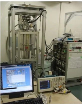
The detector and the current read out circuit were mounted on a cold stage in a dilution refrigerator with pulse-tube pre- cooling head. Our experiments ofγ-ray detection indicated that the mechanical vibration derived from the pulse-tube had great effect on the base line noise of the output cur- rent from the TES detector coupled with the heavy metal absorber. Therefore to achieve the good energy resolution, propagation of the mechanical vibration from the pulse-tube unit to the cold stage in the dilution refrigerator should be suppressed as small as possible. Figure 4 shows the pho- tograph of our dilution refrigerator system which is used for theγ-ray TES operation. The pulse-tube unit, which was suspended from a top board through several vibration dampers, is separated from the dilution Dewar vessel, and they are connected with welding bellows. Current through the TES was measured with a one-stage superconducting
Fig. 4 The dilution refrigerator with pulse-tube pre-cooling head.
quantum interference device (SQUID) current amplifier that consists of 100 series-array dc-SQUIDs. The TES is con- nected in series to the SQUID input coils and in parallel to the shunt resistor, in which resistance is much smaller than the TES resistance, such as a constant voltage bias is ap- plied to the TES. As this device showed a normal resistance of 850 mΩat 1 K, we choose a shunt resistor of 20 mΩ.
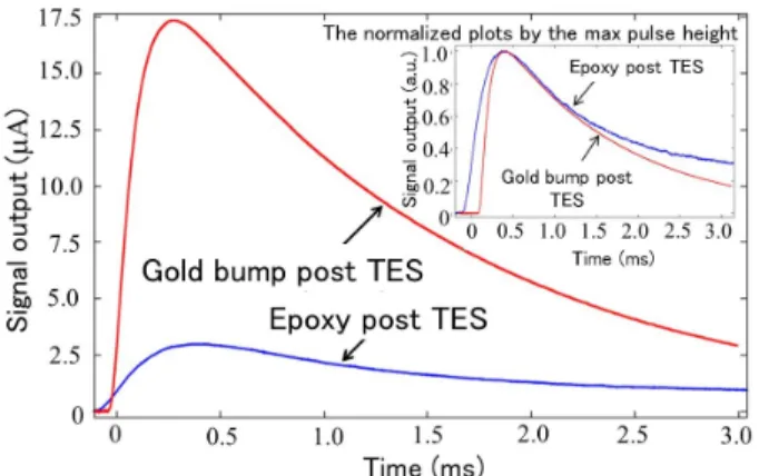
The TES was cooled to around 100 mK, and it was bi- ased at the resistance of 85 mΩ(10% of normal resistance) in the transition edge. Then theγ-rays were incident on the TES from aγ-ray source at the room temperature through a beryllium window of the dilution Dewar vessel. Figure 5 shows the measured current pulse of241Am (59.5 keV)γ-ray event. In this figure the pulse shape of the new device us- ing the gold bump post is compared with the pulse shape of the previous device using the epoxy post (Stycast 2850FT).
The pulse height of the signal of the Au bump post TES was larger than that of the epoxy post TES by more than 6 times. The inset of Fig. 5 shows the normalized plot of these pulse shapes with respect to the maximum pulse height of the Fig. 5. In the decay curve of each plot we can observe a slow component following the fast component. However the difference between the slow component and the fast compo- nent of the epoxy post TES seems to be larger than that of the gold bump post TES. The time constant of slow decay component improved from 24 ms of the epoxy post TES to less than 5 ms of the gold bump post TES. Although the ori- gin of these two time components in the decay curve is still not clearly understood, we consider that the strong thermal coupling between the Ir/Au film and the Sn absorber, which
Fig. 5 The signal current pulse of241Am (59.54 keV)γ-ray event, mea- sured by the TES with a gold bump post compering with that of the TES with the epoxy post, and the normalized plots by the max pulse height (in- set).
is brought by the high thermal conductivity of the gold bump post, may suppress the decay time constant of the slow de- cay component[7],[8].
γ-ray measurements taken by putting twoγ-ray sources of241Am and57Co together in front of the beryllium win- dow, obtained the energy spectrum as shown in Fig. 6. We observed the photopeak of241Am at 59.54 keV, and two es- cape peaks at 31.07 keV and 34.35 keV, which correspond to the escape energy loss of the Sn Kβand KαX-rays, re- spectively. And also, we observed the photopeak of57Co at 122.06 keV and the small peaks at around 95 keV, which arise from the escape events of Sn Kβand KαX-rays. In the analysis ofγ-ray spectrum obtained by the TES detector, we should pay attention to these escape events and need to clean up these artifacts. These escape events complicate identifi- cation of the nuclide much more in heavy metal materials used forγ-ray absorber than in Si (Silicon) or Ge (Germa- nium), due to the much higher energies of the characteristic X-rays. In this spectrum as shown in Fig. 5, the energy reso- lution of 59.54 keV peak is estimated to 84 eV FWHM. This resolution is more than 4 times better than the energy reso- lution of HPGe whose theoretical limit is 400 eV at 60 keV by the Fano statistics of electrons and holes, produced by the incident photons. However, our energy resolution is still limited by the low frequency noise and the mechanical vi- bration of the pulse-tube pre-cooling head of our dilution re- frigerator system dominates it. Figure 7 shows the base line noise power spectrum of this TES detector. We observed the very large noise peaks, at 873 Hz, 1.77 kHz and 2.87 kHz which is derived from the vibrations of the refrigerator, be- cause we confirmed that these noise peaks were disappeared by temporary stopping of the pulse-tube unit. These effects of the mechanical vibration on the frequency band around these noise peaks might contribute considerably to degrade the energy resolution. We consider that vibration level is much higher because our refrigerator system uses the valve motor integrated pulse-tube unit. Therefore now we are re- placing it to a pulse-tube unit, which is separated from the valve motor unit to achieve a better energy resolution.
Fig. 6 The energy spectrum of γ-ray from241Am source and 57Co source, measured by the TES with a tin absorber.
Fig. 7 The base line noise power spectrum of TES coupled with tin absorber, which cooled by the dilution refrigerator with pulse-tube pre- cooling unit.
4. Nuclear Material Measurement
To demonstrate the precision measurements of nuclear ma- terial samples by the TES coupled with a Sn absorber, we moved the dilution refrigerator integrated TES detector and the signal read out system described above, to the facilities of Japan Atomic Energy Agency (JAEA).
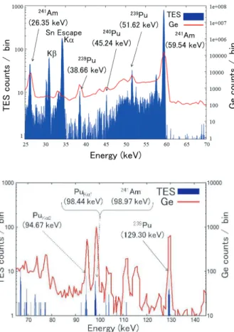
First, γ-ray measurements from a Pu nitrate sample were performed. Also, for reference of the energy spec- trum, the same Pu sample was measured by the HPGe de- tector. The energy spectrum of the TES detector comparing with that of the HPGe detector is shown in Fig. 8. In the TES spectrum, we can identify the sharp energy peaks de- rived from the 239Pu at 38.66 keV, 51.62 keV and 129.30 keV among manyγ-ray peaks. And, at 45.24 keV the en- ergy peak derived from 240Pu is also identified. On the other hand, these energy peaks from Pu nuclides cannot be confirmed or can be hardly confirmed in HPGe spectrum.
Therefore, HPGe detector cannot evaluate precisely the con- centration ratio of these Pu nuclides in this spectrum. From these results, it is notable that the TES detector has the abil- ity to identify the isotope ratio of Pu nuclides, and we expect
Fig. 8 The energy spectrum ofγ-ray from Pu sample, measured by the TES comparing with that of the HPGe detector. (upper: 25∼70 keV, lower:
70∼150 keV)
that TES detector become powerful tool of the advanced nu- clear material analysis of the next generation nuclear safe- guards. The energy peaks of characteristic X-rays emitted by Pu are also founded. We estimate the peak at 94.70 keV as Pu Kα1, and however the peak of Pu Kα2 at 98.44 keV are not completely separated fromγ-ray peak of241Am at 98.97 keV due to the statistical dispersion.
Next, we tried to measure γ-rays from nitrite solu- tions which contains Fission Products (FP) derived from the spent nuclear fuel. Although the TES detector was ex- posed by many Compton scattered photons from a137Cs, we succeeded to demonstrate the identification of the nuclides which was contained in FP sample. Figure 9 showsγ-ray energy spectrum of FP sample measured by the TES detec- tor, and also represents the energy spectrum measured by HPGe for comparison. In this spectrum we observed sev- eral energy peaks of characteristic X-rays emitted by the el- ements of Cs (Ba), and Eu (Gd), contained in FP, andγ-ray peaks of241Am,154Eu, and155Eu. It is remarkable that, in each energy peak, TES can resolve the fine structures of the fluorescence X-ray line like Kα1 and Kα2, which cannot be resolved by HPGe detector. We expect that this strong resolving power ofγ-ray energy peaks might contribute to improve the detection sensitivity of nuclides under the high background by Compton scattered events of high energyγ- rays in the assumption of the inspection of the spent nuclear
Fig. 9 The energy spectrum ofγ-ray from nitrite solutions which con- tains FP derived from the spent nuclear fuel, measured by the TES compar- ing with that of the HPGe detector. (upper: 25∼65 keV, lower: 58∼150 keV)
fuel.
5. TES Coupled with Tantalum Absorber
Improvement of the detection efficiency of γ-rays around 100 keV is expected for the nuclide analysis of Pu and ac- tinide, therefore we focus on the property of Ta, which fea- tures small heat capacity and large stopping power forγ-ray as shown in Table 1. Further, Ta has measurable absorp- tion efficiency forγ-ray energies from 500 keV to 1 MeV.
If the TES detector realizes the high energy resolution spec- troscopy in this energy range, it might be useful for Coin- cidence Doppler Broadening (CDB) Positron Annihilation Spectroscopy (PAS) studies, which gives information on the electron momentum distribution in the sample with the irra- diation damage or the lattice defect[9]–[12].
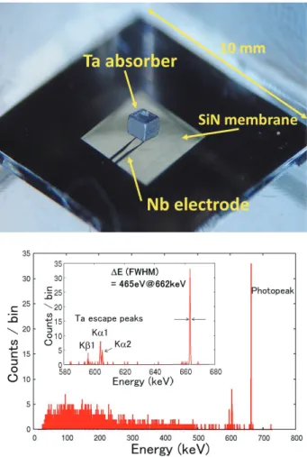
Our TES coupled with a Ta absorber was fabricated in a similar way as the TES coupled with Sn absorber[13]. Fig- ure 10 (upper photograph) shows the TES with Ta absorber of 0.5 mm×0.5 mm ×0.3 mm in size. The gold bump post connects Ta absorber to the superconducting Ir/Au bi- layer film which deposited on the silicon nitride membrane of 1µm thick. We cooled this TES sensor using the dilution refrigerator as same as before. The cold stage of the refrig- erator was maintained at 100 mK, and the measurement of
Fig. 10 The TES with a Ta absorber for Gamma-ray detection and the energy spectrum ofγ-ray from137Cs source.
γ-ray from a137Cs source was performed. We found out that the real heat capacity of this device that was calculated from the decay time constant ofγ-ray incident signal was much larger than the theoretical heat capacity. This increase of the heat capacity may be brought by the hydrogen absorption on the Ta surface as other research group pointed out[1]. In ad- dition to that, because Ta absorber is heavier than the Sn ab- sorber, the vibration of the refrigerator results a larger noise level on the TES detector and it degraded the energy resolu- tion. Theγ-ray energy spectrum measured by the TES with Ta absorber is shown in Fig. 10 (lower). We can observe a very sharp photopeak at 662 keV and the escape peaks at 596.8 keV, 604.5 keV and 605.8 keV, which correspond to the escape energy loss of the Ta Kβ, Kα1 and Kα2 X-rays, respectively. Although the energy resolution is limited by the noise derived from the vibration of the refrigerator and by the increase of the heat capacity, we achieved a good en- ergy resolution of 465 eV FWHM at 662 keV. This value is the best energy resolution in this energy range, while HPGe detector is still limited to 1.5 keV at 662 keV. Further, due to this good energy resolution and high absorption efficiency, peak-to Compton ratio reaches 30 in this spectrum, while the ratio of typical Ge detector is around 50.
absorber achieved the good energy resolution of 84 eV at 60 keV. And also our TES with Ta absorber achieved the best energy resolution of 465 eV at 662 keV. These resolution is much better than that of HPGe detector, although it is still now limited by the noise derived from the vibration of the dilution refrigerator system. Further, we performed the nuclear material measurements by using TES with Sin absorber. In the measurement of Pu nitrate sample, we suc- ceeded to identify the sharp energy peaks derived from the
239Pu and240Pu, in which HPGe detector could not identify clearly. In the measurement of FP sample, we succeeded to detect several energy peaks of characteristic X-rays emitted by the elements contained in FP andγ-ray peaks of241Am,
154Eu, and155Eu with much better energy resolution than that of HPGe detector. Based on these results, we consider thatγ-ray spectrometer using a TES detector can be applied for the advanced non-destructed inspection of the nuclide material.
Acknowledgments
This work was financially supported by “The Center of World Intelligence Project for Nuclear S&T and Human Resource Development”, Ministry of Education, Culture, Sports, Science and Technology (MEXT), and SENTAN, Japan Science and Technology agency (JST). And also this was supported by JSPS KAKENHI Grant Number 15H02341 and 26630480.
References
[1] R.D. Horansky J.N. Ullom, J.A. Beall, W.B. Doriese, W.D. Duncan, L. Ferreira, G.C. Hilton, K.D. Irwin, C.D. Reintsema, L.R. Vale, B.L. Zink, A. Hoover, C.R. Rudy, D.M. Tournear, D.T. Vo, and M.W.
Rabin, “Superconducting absorbers for use in ultrahigh resolution gamma-ray spectrometers based on low temperature microcalorime- ter arrays,” Nucl. Instrum. Methods Phys. Res. Section A, Accel., Spectrometers, Detectors Assoc., vol.579, no.1, pp.169–172, Aug.
2007.
[2] A.S. Hoover, R. Winkler, M.W. Rabin, D.T. Vo, J.N. Ullom, D.A.
Bennett, W.B. Doriese, J.W. Fowler, R.D. Horansky, D.R. Schmidt, L.R. Vale, and K. Schaffer, “Determination of plutonium isotopic content by microcalorimeter gamma-ray spectroscopy,” IEEE Trans.
Nucl. Sci., vol.60, no.2, pp.681–688, April 2013.
[3] K.D. Irwin, G.C. Hilton, D.A. Wollman, and J.M. Martinis, “X- ray detection using a superconducting transition edge sensor mi- crocalorimeter with electrothermal feedback,” Appl. Phys. Lett., vol.69, no.13, pp.1945–1947, Sept. 1996.
[4] M. Ohno, H. Takahashi, R.M.T. Damayanthi, Y. Minamikawa, and
pp.1–10, Aug. 2014.
[7] R.D. Horansky, D.A. Bennett, D.R. Schmidt, B.L. Zink, and J.N.
Ullom, “Identification and elimination of anomalous thermal decay in gamma-ray microcalorimeters,” Appl. Phys. Lett., vol.103, no.21, Nov. 2013.
[8] S. Hatakeyama, T. Irimatsugawa, M. Ohno, H. Takahashi, R.M.T.
Damayanthi, C. Otani, and T. Maekawa, “Development of Hard X- ray and Gamma-ray Detector with Transition Edge Sensor for Nu- clear Materials Analysis,” IEEE Trans. Appl. Supercond., vol.25, no.3, 2101303, June 2015.
[9] S.W. Leman and H. Takahashi, “Development of transition edge sen- sor gamma-ray detectors for positron-annihilation-spectroscopy,” J.
Low Temp. Phys., vol.151, no.3/4, pp.784–789, Feb. 2008.
[10] P. Asoka-Kuamar, M. Alatalo, V.J. Ghosh, A.C. Kruseman, B.
Nielsen, and K.G. Lynn, “Increased elemental specificity of positron annihilation spectra,” Phys. Rev. Lett., vol.77, no.10, pp.2097–2100, Sept. 1996.
[11] R.M.T. Damaynathi, S.W. Leman, H. Takahashi, M. Ohno, Y.
Minamikawa, K. Nishimura, and N. Iyomoto, “Development of a gamma-ray detector with iridium transition edge snesor coupled to a Pb absorber,” IEEE Trans. Appl. Supercond., vol.19, no.3, pp.540–
543, June 2009.
[12] R.M. Thushara Damayanthi, M. Ohno, S. Hatakeyama, H.
Takahashi, and C. Otani, “Development of bulk superconducting- absorber coupled transition-edge sensor detectors for positron anni- hilation spectroscopy,” IEEE Trans. Appl. Supercond., vol.23, no.3, 2100304, June 2013.
[13] T. Irimatsugawa, S. Hatakeyama, M. Ohno, H. Takahashi, C. Otani, and T. Maekawa, “High Energy Gamma-Ray Spectroscopy Using Transition-Edge Sensor With a Superconducting Bulk Tantalum Ab- sorber,” IEEE Trans. Appl. Supercond., vol.25, no.3, 2101303, Jan.
2015.
Masashi Ohno received the B.E. and Ph.D.
degrees, the school of Engineering the Univer- sity of Tokyo in 1999 and 2004, respectively.
He joined in RIKEN, as special postdoctoral re- searcher in 2004. During 2006–2010, he joined PRESTO program of Japan Science and Tech- nology agency (JST). He is now associated pro- fessor of Nuclear professional school, the Uni- versity of Tokyo.
Hiroyuki Takahashi received the B.S. and M.S. degrees in Nuclear Engineering, from the University of Tokyo in 1985 and 1987, respec- tively. From October 2002 through March 2005, he worked at Research into Artifacts, Center for Engineering, the Univesity of Tokyo. He is now with the Department of Nuclear Engineer- ing and Management, the Univesity of Tokyo.
Chiko Otani received his B.S. degree in Physics from Kyoto University in 1990, and his M.S. and Ph.D. degrees in astronomy from the University of Tokyo in 1992 and 1995, respec- tively. In 1995, he joined in RIKEN as a spe- cial postdoctoral researcher. Since 2005, he is a Team Leader of Terahertz Sensing and Imaging Team in RIKEN. From 2013, he is also a Group Director of Terahertz-wave Research Group in RIKEN.
Takashi Yasumune received the B.E., M.E.
and Ph.D. degrees in nuclear engineering from Kyushu University in 2007, 2009 and 2012, re- spectively. He joined Japan Atomic Energy Agency(JAEA) in 2012. He is now an engineer of Health and Safety Department in Oarai Re- search and Development Center of JAEA.
Koji Takasaki received the B.E., M.E.
and Ph.D. degrees in Nuclear Engineering, from Kyusyu University in 1984, 1986 and 2010, respectively. He is now the deputy direc- tor of Health and Safety Department in Oarai Research and Development Center of Japan Atomic Energy Agency.
Takashi Ohnishi received the B.S. and M.S.
degrees in the school of Engineering, from To- hoku university in 2006 and 2008, respectively.
He is now with Japan Atomic Energy Agency.
Shin-ichi Koyama received the B.S. and Ph.D. degrees in Faculty of Engineering from Iwate university in 1988 and school of Engineer- ing, from Tohoku university in 2007, respec- tively. He is now the deputy director of Fuku- shima Research Infrastructural Creation Center of Japan Atomic Energy Agency.
Shuichi Hatakeyama received the Ph.D. de- gree in engineering, from The University of To- kyo in 2015. During 2014–2015, he joined Re- search Fellowship for Young Scientists of Japan Society for the Promotion of Science (JSPS). He is now with Hitachi, Ltd. Research & Develop- ment Group.
R.M. Thushara. Damayanthi received the B.S. degree in Electrical Engineering, from Uni- versity of Moratuwa in 2003 and M.S. and Ph.D.
degrees in Nuclear Engineering from University of Tokyo in 2006 and 2009, respectively. Dur- ing 2013–2016, she was in RIKEN, Japan as a special postdoctoral researcher. She is now with University of Moratuwa, Sri Lanka as a senior lecturer.