INVITED PAPER
Special Section on Leading-Edge Technology of Superconductor Large-Scale Integrated CircuitsLarge-Scale Integrated Circuit Design Based on a Nb Nine-Layer Structure for Reconfigurable Data-Path Processors
Akira FUJIMAKI†, Masamitsu TANAKA†a),Members, Ryo KASAGI†, Katsumi TAKAGI†, Masakazu OKADA†, Yuhi HAYAKAWA†, Kensuke TAKATA†,Student Members, Hiroyuki AKAIKE†, Nobuyuki YOSHIKAWA††, Shuichi NAGASAWA†††, Kazuyoshi TAKAGI††††,Members,andNaofumi TAKAGI††††,Senior Member
SUMMARY We describe a large-scale integrated circuit (LSI) design of rapid single-flux-quantum (RSFQ) circuits and demonstrate several re- configurable data-path (RDP) processor prototypes based on the ISTEC Advanced Process (ADP2). The ADP2 LSIs are made up of nine Nb lay- ers and Nb/AlOx/Nb Josephson junctions with a critical current density of 10 kA/cm2, allowing higher operating frequencies and integration. To realize truly large-scale RSFQ circuits, careful design is necessary, with several compromises in the device structure, logic gates, and interconnects, balancing the competing demands of integration density, design flexibility, and fabrication yield. We summarize numerical and experimental results related to the development of a cell-based design in the ADP2, which fea- tures a unit cell size reduced to 30-μm square and up to four strip line tracks in the unit cell underneath the logic gates. The ADP LSIs can achieve∼10 times the device density and double the operating frequency with the same power consumption per junction as conventional LSIs fabricated using the Nb four-layer process. We report the design and test results of RDP pro- cessor prototypes using the ADP2 cell library. The RDP processors are composed of many arrays of floating-point units (FPUs) and switch net- works, and serve as accelerators in a high-performance computing system.
The prototypes are composed of two-dimensional arrays of several arith- metic logic units instead of FPUs. The experimental results include a suc- cessful demonstration of full operation and reconfiguration in a 2×2 RDP prototype made up of 11.5k junctions at 45 GHz after precise timing de- sign. Partial operation of a 4×4 RDP prototype made up of 28.5k-junctions is also demonstrated, indicating the scalability of our timing design.
key words: advanced process, cell-based design technique, high-end com- puting, large-scale integration, rapid single-flux-quantum circuits
1. Introduction
Rapid single-flux-quantum (RSFQ) circuits [1], [2] have key features of high-speed operation and data transmission that range up to the sub-terahertz region, with ultra-low power consumption. High-end computing, which has recently suf- fered from huge system power consumption, is an attrac- tive application area of RSFQ large-scale integrated circuits (LSIs). The development of RSFQ microprocessors was first started in the FLUX processor project [3]. We suc- cessfully demonstrated the high-speed operation of a mi- croprocessor series called CORE1 that was based on bit-
Manuscript received August 10, 2013.
Manuscript revised November 1, 2013.
†The authors are with Nagoya University, Nagoya-shi, 464- 8603 Japan.
††The author is with the Yokohama National University, Yokohama-shi, 240-8501 Japan.
†††The author is with AIST, Tsukuba-shi, 305-8568 Japan.
††††The authors are with Kyoto University, Kyoto-shi, 606-8501 Japan.
a) E-mail: masami [email protected] DOI: 10.1587/transele.E97.C.157
serial architectures [4]–[7]. Such large-scale, complex dig- ital circuits cannot be realized without advances in LSI de- sign technologies. We established a cell-based design tech- nique [8] based on the ISTEC 2.5-kA/cm2 standard pro- cess (STP2) [9]. With a cell-based design, RSFQ circuits are composed of predefined, tile-shaped primitives called
‘cells’. Our cell library includes both logic gates and wiring elements such as Josephson transmission lines (JTLs) and pulse splitters with detailed timing information. We can quickly design RSFQ circuits on ten-thousand Josephson junction (JJ) scales using a logic simulator.
In 2006, we started a project on reconfigurable data- path (RDP) processors to allow 10 teraflop desk-side com- puters [10]. An RDP is composed of many arrays of floating-point units (FPUs) connected by switching net- works. The RDP processors serve as accelerators. The data path can be reconfigured to reflect a long series of instruc- tions appearing in each loop of large-scale calculations. We can implement parallel and pipelined processing with little memory access to avoid increasing the required bandwidth between microprocessors and memories. This is known as the memory-wall problem [11]. RSFQ circuits are very suit- able as RDP processors, because their high speed and low power density allows us to use a bit-serial or bit-slice ar- chitecture. This significantly reduces the circuit scale of the components and maximizes the performance per watt of FPUs, resulting in integration of a larger number of FPUs.
Recent progress in the fabrication process at ISTEC en- abled us to make multi-layered RSFQ LSIs [12]–[14]. We developed a second-generation fabrication process featuring a critical current density of 10 kA/cm2, called the Advanced Process 2 (ADP2), in the RDP project. Our aim is to realize much larger-scale circuits, such as FPUs and RDP proto- types [15]–[17]. With an increase in critical current den- sity to 10 kA/cm2, many RSFQ LSIs have been successfully demonstrated with higher operating frequencies (e.g., [18], [19]).
Because the integration density, design flexibility, and fabrication yield compete against each other, careful con- sideration and several compromises were required to en- sure higher flexibility in the multi-layered devices, to realize truly large-scale RSFQ circuits. In this paper, we describe the LSI design in the ADP2 devices based on the cell-based design technique. In particular, we describe how we reached the current design of the device structure, logic gate cells, and passive interconnects. Then, we report on the design Copyright c2014 The Institute of Electronics, Information and Communication Engineers
the effect of the DCP layer, however, showed that the mag- netic fields were not shielded sufficiently by a single ground plane layer, and operation of large-scale circuits could be disturbed by the coupled magnetic fields [20], [21].
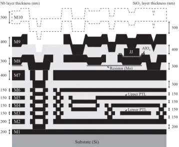
In the ADP2 LSIs, we changed the device structure and film thicknesses of the Nb layers to improve the tol- erance for dc bias currents [22]. Figure 1 shows a schematic cross-sectional view of the device structure. The PTL layers are formed between the DCP layer (M1) and main ground plane. The key concepts are: (1) keep the DCP layer as far away from the active layers as possible; (2) insert multiple grounded layers, i.e., M2, M4, and M6, to serve as ground planes for strip lines and also as shielding layers; and (3) use a thicker film for the main ground plane (M7). The ac- tive layers are not planarized, and are almost the same as the layout design based on the STP2. This means that we can use many conventional layouts and design tools, such as an inductance extractor (L-meter) [23], with little modification.
A disadvantage of this device structure is that via holes con- necting the DCP layers to active layers are required. These could occupy a large area and affect the flexibility of the
Fig. 1 Schematic cross-sectional view of the ADP2 device. The nine Nb layers are called M1, M2, ... M9 from the bottom. The tenth Nb layer (M10) is reserved for future use. In the actual device, the upper via holes become larger as they are stacked.
layer because it increased in the circuit area and power con- sumption. Instead, we introduced contacts connecting the grounded layers with each other to ensure the paths of re- turn currents. We believe that the amount and distribution of stray return currents is limited within a cell-size level.
These inter-ground contacts are placed at the fixed points of each cell because they also interfere with the PTL layers.
Moat structures, which are widely used to prevent the influence of trapped magnetic flux, also affect the flexibility of PTL interconnects. It is important to keep areas for moat structures before designing the layout of whole circuits, or we hardly find sufficient space. We describe the moat pattern design in the next subsection in detail.
The grounded layers of M6 and M7 must be formed separately so that PTL interconnects and JJs can be placed independently. This is because electrical contacts in the caldera planarization layers [12] are formed only at the edges of via holes. Another reason is different require- ments for the insulator layers under M6 and M7. The for- mer layer should be thin, and the thickness should be care- fully controlled to obtain the higher, well-defined character- istic impedance. The latter layer, referred to as the comple- mented planarization layer, should be thick enough and then carefully planarized, because the flatness is important for JJ formation.
The tenth Nb layer (M10) is reserved for future use, such as for the upper ground plane (skyplane) or low-loss PTLs. It is not implemented in the current ADP2 devices, in order to increase the fabrication yield and throughput.
2.2 Logic Gates
We first determined the unit size of the cell, which was 40μm square in the STP2. The feature sizes except for JJs, such as the minimum line width and spacing, were not changed from 1.0μm in the ADP2. However, the following factors in the advanced fabrication process contributed to a reduction in the unit size: (1) the RC-type JJs, with which we could lay out shunt resistors effectively, resulting in half the occupied area for a typical grounded JJ; (2) stacked con- tacts, which minimized the areas of via holes to supply dc bias currents, inter-ground contacts, JJs, etc.; (3) increased sheet resistance; (4) a DCP layer that eliminated dc bias sup-
Fig. 2 AND gate in the ADP2 cell library. (a) Mask layout pattern and (b) microphotograph.
ply lines on the active layers. Although our investigation of the layout design of the active layers showed that the unit size could be decreased to 25μm, we finally fixed the unit size to 30μm in consideration of other factors such as the PTL and moat structures.
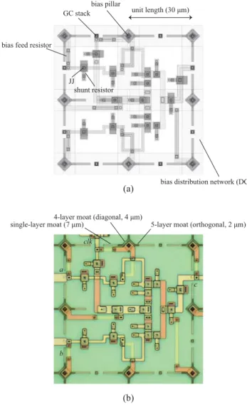
Figure 2 shows an example of the layout design and a microphotograph of the cell. The dc bias currents are sup- plied via stacked contacts between M1 and M8, called bias pillars and bias feed resistors. The size of a bias pillar is 5-μm square (the core part of the 3-μm square surrounded by a 1-μm-wide isolation spacing). A critical current of at least 5–10 mA is guaranteed by the fabrication process. We carefully designed the cells to keep the current draw from the bias pillar from exceeding 2.4 mA in any combination.
The dc bias supply lines on the M1 layer form a meshed pat- tern, which shows the advantage of dc bias margins in large- scale circuits [20]. Return currents are expected to flow via inter-ground contacts, called GC stacks, placed between the bias pillars. For the moat structure, we investigated the most effective configuration for multi-layer devices with multi-
Fig. 3 Dependence of JJ switching time on the power-suppy voltage in the STP2 and ADP2. Each set of switching times is normalized by the value when the bias voltage is high enough (i.e., the constant-current driven case).
ple ground planes [28]. Based on the experimental results, the moat structure in ADP2 cells is composed of three dif- ferent patterns that remove a single layer (M7), four layers (M7, M6, M4, M2), or five layers (M7, M6, M4, M2, M1), as shown in Fig. 2(b). The five-layer moat structure is ex- pected to be the most effective, but it must be combined with four-layer moats so as to avoid dividing the bias dis- tribution network on the DCP layer. The four-layer moat patterns are also used for electrical isolation between the bias pillar cores and ground planes. We found that these moat patterns placed at the corners of cells were not fully effective at blocking magnetic flux trapping. Because four- and five-layer moats interfere with the PTL tracks, we intro- duced single-layer moats to surround the circuits.
The circuit parameters are based on the CONNECT cells [8] that was developed for the STP2. We did not in- crease the power-supply voltage from 2.5 mV because of the power consumption. TheICRSproduct is 0.77 mV for criti- cal dumped JJs (βC=1) in ADP2 devices, whereIC,RS, and βCare the Josephson critical current, shunt resistance, and McCumber-Stewart parameter, respectively. Figure 3 shows the power-supply voltage dependence of the switching time of a JJ in a JTL obtained from numerical simulation. Be- cause a voltage of 2.5 mV is not large enough to drive a JJ with a constant current, the switching time was reduced by 12%. We decided to increaseβCto 2.0 because numerical simulations showed that there was little change in the criti- cal margins and dc bias margins of logic gates for values of βCin a range between 1.0 and 3.0 without re-optimization of circuit parameters, and that the switching speeds of higher βCJJs were increased. TheICRSproduct was 1.13 mV.
At the input and output ports of every cell, JJs with a standardIC (216μA) were placed in an almost fixed layout design, which composed JTLs between cells to ease inter- ference due to connections. We developed more than 250 cells, including logic gates and wiring cells, but excluding PTL segments (to be described later) in the ADP2 cell li- brary. We experimentally confirmed the successful opera-
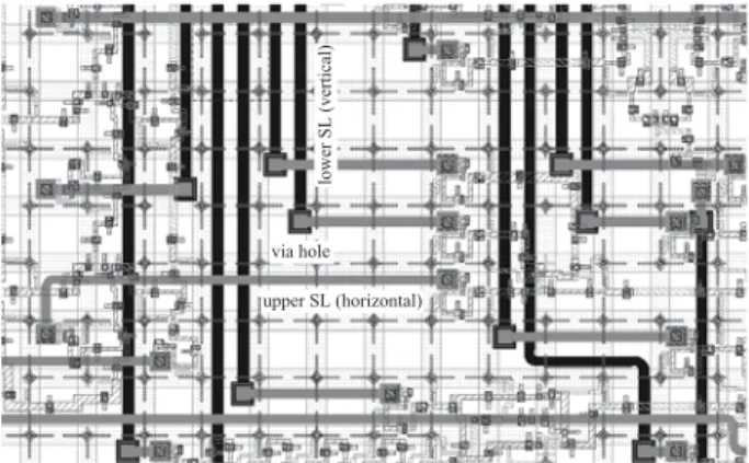
thickness is 150 nm, as shown in Fig. 1; the resultant width is approximately 5μm. The wiring density, in fact, depends on via holes between SLs because they occupy a much larger area, and also on interfering objects such as bias pillars, moats, and GC stacks. Our target in the PTL design for the ADP2 was to make two SL tracks in the same direction within the unit cell size. To make effective use of the area, we used diamond-shaped bias pillars, and shifted SL tracks toward the centers of the cells. Figure 4 shows an example layout view where we use lower SLs and upper SLs for ver- tical and horizontal wirings, and freely placed logic gates overlapping the SLs.
We set the characteristic impedance of the SLs to 5.6Ω.
A much higher characteristic impedance can lead to nar- rower SLs, but this would create overhead because high- impedance driver and receiver circuits are difficult to imple- ment by simple circuitry. The widths of the upper and lower SLs were 4.8μm and 5.5μm, respectively. The numbers of JJs at the driver and receiver circuits were 2 and 3, respec- tively. The circuit parameters were optimized to have suf- ficient margins, even at resonance frequencies. The layout design of via holes was also optimized in terms of the area and propagation properties. We allowed a smaller minimum spacing of 0.8μm on the PTL-related layers. The design detail is described in [31]. The size of a via hole was ap- proximately 12μm square. As a result, up to four SL tracks,
Fig. 4 Example of the layout view of the ADP2 LSI. Two SL tracks in the same direction can be made in the unit cell size, and overlapped with the logic gates.
semiconductor LSI design, ultra-fast RSFQ circuits require severe timing designs, and wire congestion is often caused by clock lines because every RSFQ logic gate has latch func- tionality. For this reason, unlike a typical semiconductor LSI design, place and route tasks cannot be achieved sep- arately. We are developing automated, timing-driven place and route (P&R) tools for RSFQ LSIs [32], [33]. We have successfully demonstrated the 50-GHz operation of an 8-bit carry look-ahead adder with 600 PTLs that were automat- ically routed by our preliminary tool within two minutes.
From the viewpoint of electronic design automation (EDA), additional layers to form another SL dedicated to routing clock signals would be helpful for further improvement.
3. Demonstration of Reconfigurable-Data-Path Proto- types
RDP processors are composed of many arrays of floating- point units (FPUs), and adjacent FPU arrays are con- nected with switch networks called operand routing net- works (ORNs). We change the functions of the FPUs and network configuration so that a long series of instructions appearing in each loop in a program are directly mapped to perform efficient calculations. The number of memory accesses is reduced remarkably by introducing RDP proces- sors, leading to higher computing performance. The FPUs in RDP processors are accompanied by shift registers, called transfer units (TUs), which operate in parallel to simply forwarding data to the next stage. The TUs increase the routability of the switch networks.
As a first step, we made several RDP prototypes using several arithmetic logic units (ALUs) instead of FPUs for simplicity. Figure 5 shows a block diagram of 2×2 and 4×4 RDP prototypes that we designed using the ADP2. The data were 7-bit signed integers that were processed serially. Op- erations were performed every eight clock cycles. We used another clock cycle to initialize the ALUs, to process con- secutive bit-serial data.
We implemented five functions for each ALU: addi- tion, subtraction, and logical AND, OR, and Exclusive OR (XOR). The ALU had six pipeline stages, and its target fre- quency was 50 GHz. The designed ALU was composed of about 700 JJs. The circuit area and dc bias currents were
Fig. 5 Block diagrams of the (a) 2×2 and (b) 4×4 RDP prototypes. D represents the D flip-flop for timing synchronization. The white boxes are shift registers.
1.1 mm×0.3 mm and 80 mA, respectively. Compared to our previous design using the STP2 [34], the target clock frequency was doubled, and the circuit area and number of JJs was reduced by 25–30%. The reduction in the JJ count mainly originated from modifications to the circuit design.
In the prototypes, we used multiplexer-based ORNs with non-destructive readout (NDRO) gates. We reduced the circuit area and number of JJs by aggressive use of PTLs.
Compared to the previous design [34], the circuit area and the number of JJs were reduced by 80% and 15%, respec- tively. For large-scale RDP processors, ORNs based on a modified crossbar switch could achieve better performance due to a pipelined, regular structure and higher scalability [35].
The data signals were distributed from one ORN to many ALUs. Then, the results met together at the next ORN.
Synchronizing these data signals is one of the challenges in the timing design in RDP processors. In particular, the RDP prototypes that we designed using the ADP2 required more precise timing design, because of the increased target clock frequencies. We introduced the following techniques to solve this problem: (1) routing PTLs with identical length between ORNs and ALU arrays, (2) insertion of D flip-flops (DFFs) after the output ports of ALUs for timing adjust- ment, and (3) modification of the layout of ALUs so that the lengths of PTL interconnects were as short as possible. We also changed the target clock frequency of the RDP proto- types to 40 GHz to ensure enough timing margins.
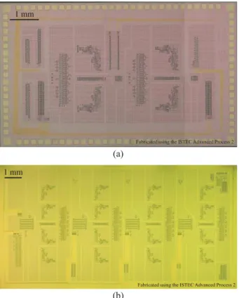
Figure 6 shows microphotographs of the 2×2 and 4×4 RDP prototypes fabricated using the ADP2. The specifica- tions are listed in Table 1. We divided the DCP layer into several islands, so that the dc bias currents were supplied to every component separately. In the design of the 4×4
Fig. 6 Microphotograph of the (a) 2×2 and (b) 4×4 RDP prototypes.
Table 1 Specifications of the RDP prototypes.
2×2 RDP 4×4 RDP
Area 5.6 mm×2.8 mm 11.0 mm×5.5 mm
JJ count 11458 28528
Total dc bias currents 1.36 A 3.34 A
Power consumption 3.4 mW 8.4 mW
RDP prototype, we inserted shift registers instead of DFFs between the ALU arrays and ORNs, which enabled us to perform detailed diagnostics.
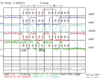
We examined operations of the RDP prototypes using on-chip high-speed tests. We successfully confirmed that every ALU could perform any operation, and every ORN could be arbitrarily configured to route data in the 2×2 RDP prototype. Figure 7 shows one of the obtained test results.
The RDP prototype processed two consecutive sets of four data inputs, and output the final results according to the given configuration. The maximum operating frequency was 45 GHz.
For the 4×4 RDP prototype, we confirmed partial op- eration at low frequencies. Even at the low-frequency tests, the timing requirement was still severe, because the circuit was designed in concurrent-flow clocking scheme. We con- firmed that the data could be transferred to the second array of the ALUs, indicating the scalability of our techniques of timing design in the RDP prototype. The circuit operation became unstable when we supplied dc bias currents to all the components, including the third and fourth ALU arrays and ORNs. We believe that this could be attributed to the
Fig. 7 Example of operation of the 2×2 RDP prototype. Input data sets were (in1,in2,in3,in4)=(1011001, 1101110, 0101010, 1010101) and (0111100, 1000111, 0001010, 1000111), and outputs were configured to out1=(in3⊕in4)+(in3⊕in4),out2=in4,out3=in2−in1, andout4= in4∧in1.
Fig. 8 Integration density of the demonstrated RSFQ LSIs using the ISTEC STP2 and ADP2.
large amount of dc bias currents. We need to reduce the total bias current by modifications such as lowering the JJ critical current and serially biasing.
The measured power consumption of the 2×2 RDP pro- totype was 3.4 mW. This was four or five orders of magni- tude smaller than when we built the same circuit with iden- tical performance using semiconductor devices. Figure 8 il- lustrates the integration density of the RSFQ LSIs, including the demonstrated RDP prototypes and several components related to the RDP such as a floating-point adder (FPA) and a floating-point multiplier (FPM) [18], comparing with LSIs based on semiconductor devices [36]. Introduction of the ADP2 led to increases in both the operating frequencies and device density by a factor of two and by a factor of ten or more. Such LSIs are thought to be very difficult to fabricate using semiconductor devices because of the power density limit.
and double the operating frequencies with the same power consumption per junction.
We reported the design and test results of RDP pro- cessor prototypes using the ADP2. The circuit area of the switch networks was drastically reduced by introduction of the ADP2, and we could implement these large-scale cir- cuits. We successfully demonstrated the 45-GHz operation of a 2×2 RDP prototype after precise timing design of each data path, with the help of higher flexibility and a shortened distance in the PTL interconnects. The experimental results of the 4x4 RDP prototype chips indicated the scalability of our timing design in RDP prototypes, but also the necessity of reducing bias currents.
Acknowledgment
The National Institute of Advanced Industrial Science and Technology partially contributed to the circuit fabrication.
This work was supported by CREST-JST, and VLSI Design and Education Center (VDEC), The University of Tokyo, in collaboration with the Cadence Corporation.
References
[1] K. Nakajima, Y. Onodera, and Y. Ogawa, “Logic design of Joseph- son network,” J. Appl. Phys., vol.47, no.4, pp.1620–1627, April 1976.
[2] K.K. Likharev and V.K. Semenov, “RSFQ logic/memory fam- ily: A new Josephson-junction technology for sub-terahertz-clock- frequency digital systems,” IEEE Trans. Appl. Supercond., vol.1, no.1, pp.3–28, March 1991.
[3] M. Dorojevets, P. Bunyk, and D. Zinoviev, “FLUX chip: Design of a 20-GHz 16-bit ultrapipelined RSFQ processor prototype based on 1.75-μm LTS technology,” IEEE Trans. Appl. Supercond., vol.11, no.1, pp.326–332, March 2001.
[4] M. Tanaka, F. Matsuzaki, T. Kondo, N. Nakajima, Y. Yamanashi, A. Fujimaki, H. Hayakawa, N. Yoshikawa, H. Terai, and S. Yorozu,
“A single-flux-quantum logic prototype microprocessor,” 2004 IEEE Int. Solid-State Circuits Conf. (ISSCC 2004) Digest of Technical Papers, no.16.7, pp.298, San Francisco, USA, Feb. 2004.
[5] M. Tanaka, T. Kondo, N. Nakajima, T. Kawamoto, Y. Yamanashi, Y. Kamiya, A. Akimoto, A. Fujimaki, H. Hayakawa, N. Yoshikawa, H. Terai, Y. Hashimoto, and S. Yorozu, “Demonstration of a single- flux-quantum microprocessor using passive transmission lines,”
IEEE Trans. Appl. Supercond., vol.15, no.2, pp.400–404, June 2005.
[6] Y. Yamanashi, M. Tanaka, A. Akimoto, H. Park, Y. Kamiya, N. Irie, N. Yoshikawa, A. Fujimaki, H. Terai, and Y. Hashimoto, “Design
and implementation of a pipelined bit-serial SFQ microprocessor, CORE1β,” IEEE Trans. Appl. Supercond., vol.17, no.2, pp.474–
477, June 2007.
[7] A. Fujimaki, M. Tanaka, T. Yamada, Y. Yamanashi, H. Park, and N. Yoshikawa, “Bit-serial single flux quantum microproces- sor CORE,” IEICE Trans. Electron., vol.E91-C, no.3, pp.342–349, March 2008.
[8] S. Yorozu, Y. Kameda, H. Terai, A. Fujimaki, T. Yamada, and S. Tahara, “A single flux quantum standard logic cell library,” Phys- ica C, vol.378–381, part 2, pp.1471–1474, Oct. 2002.
[9] S. Nagasawa, Y. Hashimoto, H. Numata, and S. Tahara, “A 380 ps, 9.5 mW Josephson 4-Kbit RAM operated at a high bit,” IEEE Trans.
Appl. Supercond., vol.5, no.2, pp.2447–2452, June 1995.
[10] N. Takagi, K. Murakami, A. Fujimaki, N. Yoshikawa, K. Inoue, and H. Honda, “Proposal of a desk-side supercomputer with reconfig- urable data-paths using rapid single-flux-quantum circuits,” IEICE Trans. Electron., vol.E91-C, no.3, pp.350–355, March 2008.
[11] W. Wulf and S. McKee, “Hitting the memory wall: Implications of the obvious,” ACM SIGArch Computer Architecture News, vol.23, no.1, pp.20–24, March 1995.
[12] K. Hinode, S. Nagasawa, M. Sugita, T. Satoh, H. Akaike, Y. Kitagawa, and M. Hidaka, “Pattern-size-free planarization for multilayered large-scale SFQ circuits,” IEICE Trans. Electron., vol.E86-C, no.12, pp.2511–2513, Dec. 2003.
[13] S. Nagasawa, K. Hinode, T. Satoh, H. Akaike, Y. Kitagawa, and M. Hidaka, “Development of advanced Nb process for SFQ cir- cuits,” Physica C, vol.412–414, no.2, pp.1429–1436, Oct. 2004.
[14] S. Nagasawa, K. Hinode, T. Satoh, H. Akaike, Y. Kitagawa, and M.
Hidaka, “Reliability evaluation of Nb 10 kA/cm2fabrication process for large-scale SFQ circuits,” Physica C, vol.426–431, pp.1525–
1532, 2005.
[15] T. Satoh, K. Hinode, S. Nagasawa, Y. Kitagawa, M. Hidaka, N. Yoshikawa, H. Akaike, A. Fujimaki, K. Takagi, and N. Takagi,
“Planarization process for fabricating multi-layer Nb integrated cir- cuits incorporating top active layer,” IEEE Trans. Appl. Supercond., vol.19, no.3, pp.167–170, June 2009.
[16] S. Nagasawa, T. Satoh, K. Hinode, Y. Kitagawa, M. Hidaka, H. Akaike, A. Fujimaki, K. Takagi, N. Takagi, and N. Yoshikawa,
“New Nb multi-layer fabrication process for large-scale SFQ cir- cuits,” Physica C, vol.469, pp.1578–1584, 2009.
[17] S. Nagasawa, K. Hinode, T. Satoh, M. Hidaka, H. Akaike, A. Fujimaki, N. Yoshikawa, K. Takagi, and N. Takagi, “Nb 9-layer fabrication process for superconducting large-scale SFQ circuits and its process evaluation,” IEICE Trans. Electron., vol.E97-C, no.3, pp.132–140, March 2014.
[18] T. Kato, Y. Yamanashi, N. Yoshikawa, A. Fujimaki, N. Takagi, K. Takagi, and S. Nagasawa, “60-GHz demonstration of an SFQ half-precision bit-serial floating-point adder using 10 kA/cm2 Nb process,” Proc. 2013 IEEE Superconductive Electronics Conference (ISEC2013), Cambridge, USA, no.PA8, July 2013.
[19] X. Peng, Y. Yamanashi, N. Yoshikawa, A. Fujimaki, N. Takagi, K. Takagi, and M. Hidaka, “Design and high-speed demonstration of single-flux-quantum bit-serial floating-point multipliers using a 10 kA/cm2 Nb process,” IEICE Trans. Electron., vol.E97-C, no.3, pp.188–193, March 2014.
[20] H. Akaike, A. Fujimaki, T. Satoh, K. Hinode, S. Nagasawa, Y. Kitagawa, and M. Hidaka, “Effects of a dc-power layer under a ground plane in SFQ circuits,” IEEE Trans. Appl. Supercond., vol.17, pp.466–469, June 2007.
[21] H. Akaike, A. Fujimaki, S. Nagasawa, Y. Kitagawa, and M. Hidaka,
“Effects of the film thickness of a ground plane in the SFQ circuits with a dc-power layer,” Supercond. Sci. Technol., vol.20, pp.S336–
S340, Nov. 2007.
[22] H. Akaike, K. Shigehara, A. Fujimaki, T. Satoh, K. Hinode, S. Nagasawa, and M. Hidaka, “The effects of a dc power layer in a 10-Nb-layer device for SFQ LSIs,” IEEE Trans. Appl. Supercond., vol.19, no.3, pp.594–597, June 2009.
[23] P.I. Bunyk and S.V. Rylov, “Automated calculation of mutual in- ductance matrices of multilayer superconductor integrated circuits,”
4th Int. Superconductive Electronics Conf. (ISEC 1993) Ext. Abs., Boulder, USA, pp.62, 1993.
[24] H. Terai, Y. Kameda, S. Yorozu, A. Fujimaki, and Z. Wang, “The effects of dc bias current in large-scale SFQ circuits,” IEEE Trans.
Appl. Supercond., vol.13, no.2, pp.502–506, June 2003.
[25] M. Tanaka, H. Akaike, and A. Fujimaki, “Control of return current flows in the single-flux-quantum circuits using positive/negative bias supply lines,” Physica C, vol.469, no.15-20, pp.1666–1669, 2009.
[26] V.K. Semenov (private communication).
[27] H. Terai, S. Yorozu, A. Fujimaki, N. Yoshikawa, and Z. Wang, “Sig- nal integrity in large-scale single-flux-quantum circuit,” Physica C, vol.445–448, pp.1003–1007, Oct. 2006.
[28] K. Fujiwara, S. Nagasawa, Y. Hashimoto, M. Hidaka, N. Yoshikawa, M. Tanaka, H. Akaike, A. Fujimaki, K. Takagi, and N. Takagi, “Re- search on effective moat configuration for Nb multi-layer device structure,” IEEE Trans. Appl. Supercond., vol.19, no.3, pp.603–606, 2009.
[29] H. Akaike, M. Tanaka, K. Takagi, I. Kataeva, R. Kasagi, A. Fujimaki, K. Takagi, M. Igarashi, H. Park, Y. Yamanashi, N. Yoshikawa, K. Fujiwara, S. Nagasawa, M. Hidaka, and N. Tak- agi, “Design of single flux quantum cells for a 10-Nb-layer process,”
Physica C, vol.469, no.15–20, pp.1670–1673, 2009.
[30] Y. Yamanashi, T. Kainuma, N. Yoshikawa, I. Kataeva, H. Akaike, A. Fujimaki, M. Tanaka, N. Takagi, S. Nagasawa, and M. Hidaka,
“100 GHz demonstrations based on the single-flux-quantum cell li- brary for the 10 kA/cm2Nb multi-layer process,” IEICE Trans. Elec- tron., vol.E93-C, no.4, pp.440–444, April 2010.
[31] K. Takagi, M. Tanaka, S. Iwasaki, R. Kasagi, I. Kataeva, S. Nagasawa, T. Satoh, H. Akaike, and A. Fujimaki, “SFQ propaga- tion properties in passive transmission lines based on a 10-Nb-layer structure,” IEEE Trans. Appl. Supercond., vol.19, no.3, pp.617–620, 2009.
[32] M. Tanaka, S. Takeshima, K. Takagi, H. Akaike, A. Fujimaki, N. Yoshikawa, S. Nagasawa, and N. Takagi, “Multi-layered single- flux-quantum circuits designed using timing-driven automatic rout- ing,” Superconductivity Centennial Conference (SCC 2011), no.1- EB-O7, The Hague, The Netherlands, Sept. 2011.
[33] K. Takagi, N. Kito, and N. Takagi, “Circuit description and design flow of superconducting SFQ logic circuits,” IEICE Trans. Electron., vol.E97-C, no.3, pp.149–156, March 2014.
[34] S. Iwasaki, M. Tanaka, Y. Yamanashi, H. Park, H. Akaike, A. Fujimaki, N. Yoshikawa, N. Takagi, K. Murakami, H. Honda, and K. Inoue “Design of a reconfigurable data-path prototype in the single-flux-quantum circuit,” Supercond. Sci. Technol., vol.20, no.11, pp.S328–S331, 2007.
[35] I. Kataeva, H. Akaike, A. Fujimaki, N. Yoshikawa, N. Takagi, K. Inoue, H. Honda, and K. Murakami, “An operand routing net- work for an SFQ reconfigurable data-paths processor,” IEEE Trans.
Appl. Supercond., vol.19, no.3, pp.665–669, 2009.
[36] T. Nakamura and Y. Mishima, “Ultra-high-speed electronics,” pp.5–
8, Corona Publishing, Japan, 2003. (in Japanese)
and Ph.D. degrees in electronics and informa- tion electronics from Nagoya University, Na- goya, Japan, in 2003 and 2006, respectively. He was a JSPS Research Fellow from 2005 to 2007.
He joined Department of Information Engineer- ing, Nagoya University in 2007, and moved to Department of Quantum Engineering in 2010, where he is currently a designated lecturer. In 2011 he was a research scholar at the University of California, Berkeley, CA, USA. His research interests include the ultra-fast/energy-efficient computing using RSFQ cir- cuits and logic design methodologies.
Ryo Kasagi received the B.E. and M.E.
degrees in electronics and quantum engineer- ing from Nagoya University, Nagoya, Japan, in 2008 and 2010, respectively. His interests include parallel signal processing toward the reconfigurable data-path processors based on rapid single-flux-quantum circuits.
Katsumi Takagi received the B.E. and M.E.
degrees in electronics and quantum engineer- ing from Nagoya University, Nagoya, Japan, in 2007 and 2009, respectively. His inter- ests include a high-speed communication tech- nique using superconductive passive transmis- sion lines in rapid single-flux-quantum circuits with a multi-layered structure.
Masakazu Okada received the B.E. and M.E. degrees in electronics and quantum en- gineering from Nagoya University, Nagoya, Japan, in 2010 and 2012, respectively. His in- terests include advanced signal processing based on rapid single-flux-quantum circuits using the reconfigurable data-path processors.
slice microarchitectures.
Hiroyuki Akaike received the B.E., M.E., and Ph.D. degrees in electronic engineering from Nagoya University in 1990, 1992, and 1995, respectively. Since 1995, he has been with Nagoya University, where he is currently an associate professor. In 2003, he stayed in Su- perconductivity Research Laboratory, ISTEC to be engaged in the development of Nb advanced fabrication process for a year. He has been in- volved in the research of superconducting de- vices and fabrication processes. He is a member of the Japan Society of Applied Physics.
Nobuyuki Yoshikawa received the B.E., M.E., and Ph.D. degrees in electrical and com- puter engineering from Yokohama National University, Japan, in 1984, 1986 and 1989, re- spectively. Since 1989, he has been with the De- partment of Electrical and Computer Engineer- ing, Yokohama National University, where he is currently a professor. His research interests in- clude superconductive devices and their appli- cation in digital and analog circuits. He is also interested in single-electron-tunneling devices, quantum computing devices and cryo-CMOS devices. Prof. Yoshikawa is a member of the Japan Society of Applied Physics, the Institute of Electrical Engineering Japan, and the Institute of Electrical Electronics Engineers.
Shuichi Nagasawa received the M.S.
and Dr. Eng. degrees from Nagoya University, Japan, in 1983 and 1998. He has been engaged in research on superconducting integrated cir- cuits, especially on Josephon RAMs since he joined NEC Corporation in 1983. From 1998 to 2013, he was on loan to Superconducting Re- search Laboratory, ISTEC, where he was en- gaged in research of single flux quantum (SFQ) circuits and the development of their fabrication process. Since 2013, he has been working at AIST, where he has been engaged in development of a fabrication process for superconducting integrated circuits. Dr. Nagasawa is a member of the Japan Society of Applied Physics.
Kazuyoshi Takagi received the B.E., M.E.
and Dr. of Engineering degrees in information science from Kyoto University, Kyoto, Japan, in 1991, 1993 and 1999, respectively. From 1995 to 1999, he was a Research Associate at Nara In- stitute of Science and Technology. He had been an Assistant Professor since 1999 and promoted to an Associate Professor in 2006, at the Depart- ment of Information Engineering, Nagoya Uni- versity, Nagoya, Japan. He moved to Depart- ment of Communications and Computer Engi- neering, Kyoto University in 2011. His current interests include system LSI design and design algorithms.
Naofumi Takagi received the B.E., M.E., and Ph.D. degrees in information science from Kyoto University, Kyoto, Japan, in 1981, 1983, and 1988, respectively. He joined Kyoto Univer- sity as an instructor in 1984 and was promoted to an associate professor in 1991. He moved to Nagoya University, Nagoya, Japan, in 1994, and was promoted to a professor in 1998. He returned to Kyoto University in 2010. His cur- rent interests include computer arithmetic, hard- ware algorithms, and logic design. He received Japan IBM Science Award and Sakai Memorial Award of the Information Processing Society of Japan in 1995, and The Commendation for Science and Technology by the Minister of Education, Culture, Sports Science and Technology of Japan in 2005.