PAPER Special Section on Design Methodologies for System on a Chip
Programmable Analog Calculation Unit with Two-Stage Architecture: A Solution of Efficient Vector-Computation
Renyuan ZHANG†a), Takashi NAKADA†,Members,andYasuhiko NAKASHIMA†,Fellow
SUMMARY A programmable analog calculation unit (ACU) is de- signed for vector computations in continuous-time with compact circuit scale. From our early study, it is feasible to retrieve arbitrary two-variable functions through support vector regression (SVR) in silicon. In this work, the dimensions of regression are expanded for vector computations. How- ever, the hardware cost and computing error greatly increase along with the expansion of dimensions. A two-stage architecture is proposed to organize multiple ACUs for high dimensional regression. The computation of high dimensional vectors is separated into several computations of lower dimen- sional vectors, which are implemented by the free combination of several ACUs with lower cost. In this manner, the circuit scale and regression error are reduced. The proof-of-concept ACU is designed and simulated in a 0.18µmtechnology. From the circuit simulation results, all the demon- strated calculations with nine operands are executed without iterative clock cycles by 4960 transistors. The calculation error of example functions is below 8.7%.
key words: approximate computing, analog calculation unit, support vector regression, vector-computation
1. Introduction
The road-map of very large scale integrated (VLSI) circuit scaling-down is approaching the end due to the physics bound. The application engineers will hardly harvest the benefit on high performance computing from higher integra- tion and frequency in the near future. Meanwhile, the de- mands on big (even huge) data processing keep increasing.
In this sense, more scalable and efficient computing systems are expected[1]. The approximate computing technology, which allows a reasonable loss of accuracy but achieves high speed and low power with lower hardware cost, is consid- ered as a promising option of efficient computing systems [2], especially on the edge devices of internet of things (IoTs) [3]. By applying the approximate computing technologies, many works have reached the rich trade-off between pre- cision and implementation cost in various real-world tasks such as pattern recognition[4]and machine learning[5]. In those works, it was found that the acceptable loss of com- putational accuracy has not significant impacts on the final performance of entire tasks.
In order to approximately but efficiently process mas- sive data, efforts on both sides of software and hardware were made for different benefit features[6]. One of typi- cal strategies is to carry out calculations by using inexact
Manuscript received September 5, 2018.
Manuscript revised January 14, 2019.
†The authors are with Nara Institute of Science and Technology, Ikoma-shi, 630-0192 Japan.
a) E-mail: [email protected] DOI: 10.1587/transfun.E102.A.878
or faulty circuits [7]. Obviously, the common concern is that the impact of cost reduction must compensate (or more commonly, over compensate) the loss of precision. Some conventional analog calculating circuits have been proved sufficiently fast, low power, and compact for specific func- tions such as multiplication [8]. However, the benefit of those function-specialized analog calculators is easily eaten up by the very poor programmability. More generally, the programmable and function flexible calculators are still de- manded. The simplest methodology of general purpose ap- proximate calculators is reducing the big-width of conven- tional digital processors[9], which hardly breaks through the trade-off between gain and loss. For greatly speeding up flex- ible calculations, the target functions can be retrieved by the look-up table (LUT) with analog addressing[10]. When the efficient memory blocks such as multi-valued logic (MVL) memories are employed, the LUT-based calculators are even scaled down in further [11]. However, the increment of operands leads to the explosion of LUTs. Therefore, those LUT-based approximate calculators are difficult to use for simultaneous vector calculations. An attempt to avoid LUT explosion was made by approximately retrieving functions with neural network (NN) on chip instead of the LUT with full patterns[12]. Although NNs are helpful to reduce hard- ware cost, only several simple functions are available due to the limitation of a small scale of NN. From our early study [13], it is feasible to retrieve arbitrary complex functions in continuous-time and compact circuit scale by implement- ing advanced regression algorithms such as support vector regression (SVR). A programmable analog calculation unit (ACU) with only 600 transistors was presented for various computations with two analog operands.
In this work, the proposed ACU is expended to vector calculations. The increment of inaccuracy and hardware cost is illustrated when the number of operands increases. Since the calculations are carried out by regressing the listed sam- ples through SVR, the accuracy and circuit scale strongly depend on the number of support vectors (SVs, known as significant samples). Unfortunately, even if the proposed efficient scheme of SVR is applied, it is very challenging to reduce the number of SVs in further if the operands are too many. Therefore, a two-stage architecture is developed to separate a complex multi-variable function into several groups with fewer variables. The free combination of ACUs is implemented to address specific target functions. In this manner, the high dimensional regression is implemented by a compact analog circuitry with improved accuracy. A proof- Copyright © 2019 The Institute of Electronics, Information and Communication Engineers
ZHANG et al.: PROGRAMMABLE ANALOG CALCULATION UNIT WITH TWO-STAGE ARCHITECTURE: A SOLUTION OF EFFICIENT VECTOR-COMPUTATION 879
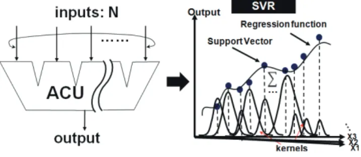
Fig. 1 Programmable ACU accepts multiple analog inputs and retrieves arbitrary functions through SVR algorithms on-chip.
of-concept ACU with nine operands is designed and simu- lated in a 0.18µm standard CMOS technology along with the interfaces between two stages and the special configu- ration of SVR training. The entire ACU consists of 4960 transistors. From the circuit simulation results, all the exam- ple functions including 3×3 convolutions and square-root with nine variables are computed in continuous-time with the calculation errors below 8.7%.
2. Prototype of Programmable ACU
A programmable ACU approximately computes arbitrary functions withNanalog inputs without any iteration of clock cycles. The SVR algorithm with Gaussian kernel[14]is real- ized by VLSI circuits to retrieve complex functions through Ndimensional regression as shown in Fig. 1. A set of sam- ple patterns including variables and correct function values are necessary for training the regression network. After the training process, the well organized regression network is ex- pected to “predict” the function value when the test patterns (variables) arrive. Giving a set of N dimensional sample vectors (X1,z1),(X2,z2),· · ·,(Xn,zn), where Xi ∈ RN is the sample vector andz∈Ris the target function value, the regression for an unknown variableXis expressed by:
f(X)=
l
X
i=1
(αi−α∗i)ex p(−γ|X−Xi|2)+b, (1) through the fundamental of SVR theory. The training pro- cess of SVR is to identify support vectors (SVs, those with non-zero parameters(α−α∗)) and corresponding parame- ters, which is out of the scope of this paper. The LIBSVM platform[15]is employed to train the SVR network. Obvi- ously, more SVs lead to the high accuracy but increase the hardware cost. Thus, an efficient scheme of SVR is proposed to reasonably reduce the number of SVs.
2.1 Efficient Scheme of SVR
The retrieval of target function is a special application of regression. The learning samples are generated from the pre-computation of the specific target functions. Namely, the resolution of sampling is alterable, but leads to the trade- off between regression accuracy and costs. In the task of
this work, the number of samples greatly impacts the num- ber of SVs which address particular circuity sets to process them. The efficient scheme of SVR is expected to achieve reasonably high accuracy with reduced SVs. A multi-round training process is introduced to evaluate each SV and elim- inate insignificant SVs as follows.
1: Regression samples are listed in a fine resolution asN dimensional vectors;
2: train the SVR model initially, observe the multiplier(αi−α∗i)for all the SVs;
3: eliminate one SV with the smallest value of parameter|αi−α∗i|; 4: replace training samples by the surviving SVs, return to step 2;
5: stop when the number of survivals is reduced to 10×N;
Finally, the surviving SVs are expected to have the most significant impact on the regression. The final number 10×N of SVs is determined from the trade-off between the accuracy and circuit scale.
2.2 Circuit Implementation
The circuit organization of ACU is described in Fig. 2. The entire ACU consists of a set of Gaussian kernel circuits and a mixer. Receiving the well-trained parameters from software side, the kernel circuits are tuned to correspond different functions. The kernel circuit is designed by a set of p- and n-type MOS transistors with amplifier factors ofKpandKn, respectively. AnNdimensional vector in analog voltages of Vi =(vi1, vi2, . . . , vi N)andVj =(vj1, vj2, . . . , vj N)is input as the operand. Nsets of squaring generators are designed to approximately calculate the square functions between each pair of input voltages. For instance, the square-subtract function betweenvi1andvj1is reflected by the currentI1orI2 for the first dimension. Assumingvi1is higher thanvj1,vi1is boosted by a sufficiently small bias current to compensate the threshold voltage of n-type MOS transistor. In this manner, the current I1 is generated by I1 = β(vi1 −vj1)2, where
β= KnKp
(√
Kp+√
Kn)2 andI2is zero. Whenvj1is higher thanvi1, I2 = β(vj1−vi1)2andI1is zero. By collecting the current from all the dimensions as Isqr = βPN
k=1|vik−vjk|2, a current-to-voltage (I-V) converter biased by a sufficiently small currentIbis used to convertIsqrinto voltage asVdi f f = V0 −γP64
k=1|vik−vjk|2, where V0 = Vd d+Vb i a s2 − |Vt h p| and
γ = Kn
(Vd d−Vb i a s− |Vt h p|)(√
Kp+√
Kn)2. The threshold voltage of p-type MOS transistor is denoted byVth p. In the block of exponential generation,Vr e f is biased to compensate the influence ofV0 (which can be easily generated by another exactly same I-V converter without any input current). Then, the output current Ioutis given in Iout = 1+eIc∆V ≈ I2ce−∆V. Finally, the result is output in the current mode as:
Iout≈ Ic
2e−γ| |Vi−Vj| |2, (2)
where I2c reflects the the parameter (αi −α∗i). Since all
Fig. 2 Circuit organization of ACU along with schematic of Gaussian kernel circuit (modified from[13]).
the results from Gaussian kernels are in the current mode, it is easy to mix them into the SVR expression by a simple current-mirror based collector:
Ir egr ession=10NX
i=1
I(αi−α∗
i)
2 e−γ| |Vi n−VSV i| |2+Ibias. (3) To program the ACU and specify a target function, a set of voltages for SVs and corresponding current Ic are applied to the kernel circuits according to the training results from the software side. The power gating technology is also sug- gested to eliminate the static power consumption from our previously presented paper[13]. Several examples are seen in Fig. 3 to illustrate various calculations by ACU, which are from the circuit simulation results. Two examples in Fig. 3(a) show the regression of cosine and exponential func- tions with the average error less than 1.5%. The calculation is processed in continuous-time with a delay less than 370ns. Another example in Fig. 3(b) shows the circuit simulation re-
Fig. 3 Circuit simulation results of ACU[13]: (a) one dimensional re- gression for cosine and exponential functions; and (b) redtwo dimensional regression forf(x1,x2)=q
x12+x22.
sult of Ndimensional regression f(x1,x2) =q
x21+x22. In this example, 20 SVs are employed to retrieve square-root function with the average error of 4.3% and the delay of 410ns. The entire ACU for two-input calculations consists of 600 transistors.
2.3 Expansion of Operands
Multi-operand calculations are implemented by simply in- creasing the number of dimensions and kernels. For instance, 9-D regressions are realized by the proposed ACU with 90 kernels, which are implemented by 9460 transistors. Com- pared with our previous work of 2-D regression (600 transis- tors[13]), the circuit scale and inaccuracy greatly increase.
Three examples of 9-input functions are illustrated by the cir- cuit simulations as shown in Fig. 4. In order to verify the non- linear regression, the first example is given by the square- root function as : f(x1,x2, . . . ,x9) =q
x21+x22+· · ·+x29. From the circuit simulation results, the average regression error for this function is 10.8%. Other two examples are in- troduced as the typical convolution kernels in applications of computer vision[16]. The Prewitt filter for edge-detection is performed as f(x1,x2, . . . ,x9)=−x1−x4−x7+x3+x6+x9 with the average error of 5.4%; the Gaussian filter for blur- ring is performed as f(x1,x2, . . . ,x9)=161 (x1+2x2+x3+ 2x4+4x5+2x6+x7+2x8+x9)with the average error of 6.5%. Since the expansion of inputs is realized by increasing the dimensions and numbers of Gaussian kernels in paral- lel, the processing delay does not noticeably differ from 1-D (370ns) to 2-D (410ns), even 9-D regression (390ns). To retrieve functions of high dimensional vectors, the necessary
ZHANG et al.: PROGRAMMABLE ANALOG CALCULATION UNIT WITH TWO-STAGE ARCHITECTURE: A SOLUTION OF EFFICIENT VECTOR-COMPUTATION 881
Fig. 4 Number of operands increases to nine for functions of square-root, Prewitt and Gaussian filters (with a size of 3×3).
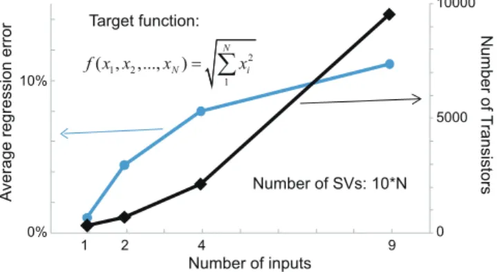
Fig. 5 For hardware implementation of high dimensional regression, in- accuracy and circuit scale greatly increase.
number of SVs increases from the fundamental of SVR the- ory. At the same time, the scale of kernel circuit addressing a specific SV also increases. Figure 5 shows the increment of average error and number of transistors for the non-linear functionq
PN
i=1x2i when N increases. For simultaneously computing the function with multiple inputs, all the kernel functions are executed in fully parallel. On the other hand, it is difficult to reduce the number of kernels due to the in- accuracy of regression. Therefore, the circuit scale is hardly reduced for a single large network of regression.
3. Two-Stage Architecture of ACU for Efficient Vector Calculation
3.1 Circuitry Organization
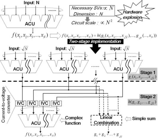
In many application fields of approximate computing such as image processing and machine learning, fast and efficient calculation of vectors is demanded. To efficiently implement the simultaneous calculation with multiple operands, a two- stage architecture of ACU is proposed as shown in Fig. 6.
TheN dimensional regression is separated into√
N groups of√
Ndimensional regressions in the first stage; then, an ad- ditional√
N dimensional regression is employed to retrieve target function in the second stage. For many applications such as convolutions, the second stage of regression can be
substituted by a linear combination of results from the first stage, which is simply implemented by the current collection.
Since the inputs of ACU are voltage signals but the output is in the current mode, an interface circuit between two stages is necessary to convert the current to voltage. The current- to-voltage (IV) converter is described in Fig. 7. Only three transistors are needed to perform the linear conversion from input currentIin to output voltageVout. The transistor M1 is biased by a sufficiently small currentIb. Then, the drain- to-source voltage of M1 isVds=VX≈Vbias−Vthn, where VbiasandVthnare a constant bias voltage and threshold volt- age of N-type MOS transistor, respectively. SinceVout is lower thanVx, M1 always operates in the linear region as:
Vout≈ Iin
K(Vbias−Vthn) +Vbias+Vthn
2 . (4)
A typical current-to-voltage characteristics is given by the circuit simulation results in Fig. 8. It is noticed that the output voltage of IV-converter does not cover the full range of input for ACU. Thus, the regression of the second stage is regular- ized ash(x10,x20, . . . ,x0√
N), where the mappingxi0=axi+b is obtained by the observation of IV-converter. More so- phisticated IV-converter circuits can also be applied for a higher quality and wider range of conversion with the small overhead. However, the conversion range is convenient to compensate by SVR; and the acceptable distortion of con- version has no serious impact on the final results.
3.2 Circuit Simulations
For proof-of-concept, an ACU processor with two-stage ar- chitecture is designed and simulated for arbitrary calcula- tions with nine operands. In this case, each ACU in both stages is implemented for three dimensional regression with 30 Gaussian kernel circuits. Four ACUs are organized as the entire processor consisting of 4960 transistors, which is about half of the prototype. Three examples are demon- strated as shown in Fig. 9. Exactly same functions as those for verifying the prototype are introduced to investigate the accuracy. Since the nine dimensional calculation is sepa- rated into three groups of regression, each regression task is
Fig. 6 Two-stage architecture of ACU is designed to separate complex functions with multiple vari- ables into several groups of lower dimensional regressions.
Fig. 7 Current-to-voltage converter is necessary between two stages of ACUs.
realized by the SVs with three-dimension. For the square- root calculation (example 1), the first stage of regression corresponds to three sets of square-summation functions;
the second stage corresponds to a root-summation function.
For the calculations of 3×3 filters, the second stage is simple summation instead of SVR. From the simulation results, the regression errors for all the examples are slightly reduced, and the processing delay of 385nsis similar to that of pro- totype. As a minor benefit of two-stage architecture, the SVR training time (considered as “synthesis” of calculation circuits) is also reduced due to the reduction of initial sam- ples and dimensions. In 9-D regression examples, the SVR training time through the LIBSVM-platform on exactly same computer server is reduced from 40sto 7sby using the two-
Fig. 8 Circuit simulation result of current-to-voltage converter shows the linearity between input current and output voltage.
stage regression. There is a potential to expand our proposed ACU to even higher dimensions by employing a hierarchi- cal architecture with multiple stages if necessary. On the other hand, the multi-stage regression is made by mapping the target function into multi-layer combinations of Gaus- sian kernels. The analog implementations of those kernels are inherently faulty. Thus, inaccuracy of kernels is accumu-
ZHANG et al.: PROGRAMMABLE ANALOG CALCULATION UNIT WITH TWO-STAGE ARCHITECTURE: A SOLUTION OF EFFICIENT VECTOR-COMPUTATION 883
Fig. 9 Circuit simulation results of calculation with nine operands as functions of square-root, Prewitt and Gaussian filters (with a size of 3×3), which are slightly improved from that of prototype.
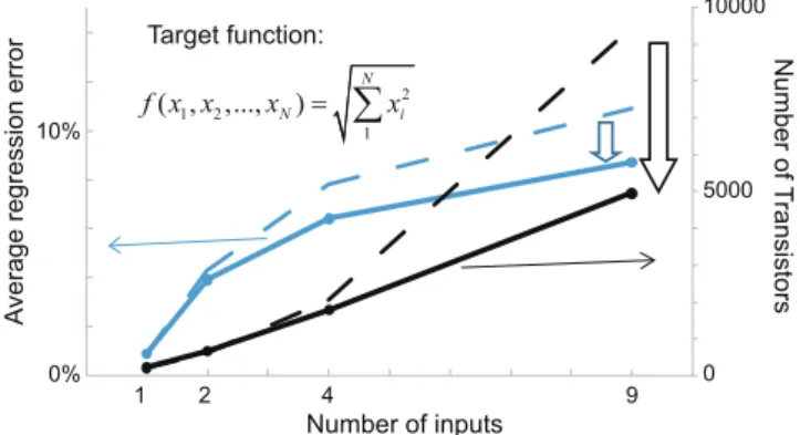
Fig. 10 Increment of circuit scale and regression error is slowed down by applying two-stage architecture. Broken lines are number of transistors and average error for prototype of ACU; and solid lines denote those for two-stage architecture.
lated from each layer to the end. From the results in Fig. 10, the error accumulation is compensated by the reduction of dimensions. However, when the number of stages increases, the error would accumulate faster than the compensation. In this sense, the multi-stage ACUs are only suggested for the applications with robust fault-resilience.
The two-stage architecture can be applied to execute the regressions of different dimensions. It is helpful to re- duce the hardware cost and inaccuracy in general. Figure 10 shows that the increment of circuit scale and regression error is slowed down by applying the proposed two-stage archi- tecture. For N-operand implementations, the number of transistors increases asO(N), which isO(N2)for the pro- totype. This fact offers the option to expand the operands in further with an acceptable hardware cost. Benefited by the reduction of circuit scale, the power consumption of ACU is also reduced. For the prototype of ACU with single stage, the operating power greatly increases from 0.011mWto 3.6mW when the number of dimensions increase from one to nine.
By applying two-stage architecture, the power for 9-D re- gression is reduced to 0.88mW. On the other hand, directly regressing high dimensional samples is very challenging and risky on the side of regression algorithms. When the number of dimensions increases, the regression error and machine
learning time will exponentially increase. Thus, partitioning the dimensions into reasonable groups is helpful to limit the regression error.
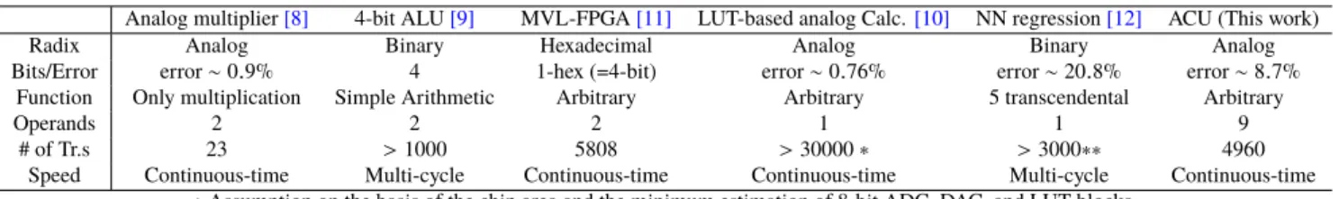
3.3 Comparisons
The comparison among several strategies for circuit imple- mentations of approximate computing is given in Table 1.
Our proposed ACU is the only processor offering simulta- neous calculations with multiple (more than two) operands.
The conventional analog calculators such as multipliers are usually very compact but the available functions are special- ized and limited. Simply reducing the bit-width of conven- tional binary processors hardly escapes from the trade-off between the cost and performance. The LUT-based calcu- lators (both of binary and MVL) are helpful to improve the speed but suffer from the scale explosion problem. The Neural-Network (NN) -regression indicates a potential to shrink look-up table. However, due to inherent property of simple NN algorithms, the functional complexity and number of operands are limited. Our ACU can be consid- ered a further effort by implementing regressions on-chip through advanced regression algorithms such as SVR. Com- plex functions of high dimensional vectors (in this paper, demonstrated by nine-dimension but can be even increased) are realized by a sets of ACUs with 4960 transistors in total.
Due to the compact circuit scale, a large number of ACUs can be integrated in parallel for the applications such as image processing.
3.4 Discussions
Similarly to most of approximate computing hardware, the use of AUCs depends upon the application fields. There is no unique golden answer on the boundary or threshold of calculating accuracy[17]. However, some surveys reported that the quality of service (QoS) is roughly linear to the computational error when the average error is less than 10%, especially in the domain of computer vision[18]. By trading the implementation cost, users may adapt (or not) ACUs according to the expected QoS limitation.
The proposed two-stage architecture is suggested to in-
Table 1 Comparisons among various strategies for circuit implementations of approximate computing.
Analog multiplier[8] 4-bit ALU[9] MVL-FPGA[11] LUT-based analog Calc.[10] NN regression[12] ACU (This work)
Radix Analog Binary Hexadecimal Analog Binary Analog
Bits/Error error∼0.9% 4 1-hex (=4-bit) error∼0.76% error∼20.8% error∼8.7%
Function Only multiplication Simple Arithmetic Arbitrary Arbitrary 5 transcendental Arbitrary
Operands 2 2 2 1 1 9
# of Tr.s 23 >1000 5808 >30000∗ >3000∗∗ 4960
Speed Continuous-time Multi-cycle Continuous-time Continuous-time Multi-cycle Continuous-time
∗Assumption on the basis of the chip area and the minimum estimation of 8-bit ADC, DAC, and LUT blocks.
∗∗Estimated by the chip area of 3578.5µm2in a 45nmtechnology.
crease number of dimensions for vector calculations. The mandatory constraint of utilization lies on the feature of tar- get function: the elements in the vector calculations should be separable. Namely, the function should be able to rep- resent by several independent components, which are im- plemented by corresponding ACUs. Fortunately, most of widely used functions in the real-world applications satisfy this constraint as such convolution, vector production, sum- mation etc. In term of accuracy, the beneficial condition of two-stage ACU lies on the number of dimensions. For the calculations of low dimensional vectors, nine for instance, the proposed two-stage architecture performs higher accu- racy over all the test functions. For the calculations of very high dimensional vectors, two-stage architecture is benefi- cially effective for the functions which can be expressed as the linear combination in the second mapping layer. Nowa- days, most of very high dimensional vector calculations such as image filters or convolution kernels (typically, from 9- to 121-D)[16]meet this beneficial condition.
The future challenge of AUCs lies on the development of specific memory system to “store” the target functions in terms of analog values. An analog memory block or an ordi- nary digital memory along with digital-to-analog converters can be applied to perform such a memory system with some overhead. Due to small size, a large amount of ACUs are expected to build in silicon with same but parallel functions.
Then, the function-oriented memories are shared by all or many ACUs to eat up the overhead. In this sense, a reason- ably high parallelism is suggested in real-world applications of ACUs.
4. Conclusion
In order to efficiently implement approximate calculations of vectors in general, the programmable analog calculation unit is developed in this work. From our early feasibility study, arbitrary functions can be approximately retrieved through the support vector regression algorithm implemented on- chip. However, the circuit scale and calculation error greatly increase when the number of operands increases. A two- stage architecture is proposed to separate the target functions with multiple variables into several groups of regressions with fewer dimensions. The free combination of multiple ACUs is applied to realize corresponding regressions. A current-to-voltage is also designed as the interface between two ACUs. The proof-of-concept processor for arbitrary cal- culations with nine operands is designed and simulated in a
0.18µmstandard CMOS technology. The entire processor consists of 4960 transistors. Several example functions in- cluding 3×3 filters and square-root functions are employed to verify the behavior of proposed ACU. All the functions are retrieved in continuous-time with the error below 8.7%.
Acknowledgments
This work was supported by JST, PRESTO Grant Number JPMJPR18M7, Japan. The authors would like to thank the VLSI Design and Education Center (VDEC) of the Uni- versity of Tokyo in collaboration with Rohm Corporation, Synopsys, Inc., and Cadence Design Systems, Inc.
References
[1] H. Hu, Y. Wen, T.-S. Chua, and X. Li, “Toward scalable systems for big data analytics: A technology tutorial,” IEEE Access, vol.2, pp.652–687, May 2014.
[2] R. Nair, “Big data needs approximate computing: Technical perspec- tive,” Commun. ACM, vol.58, no.1, p.104, 2015.
[3] M. Gao, Q. Wang, M. Arafin, Y, Lyu, and G, Qu, “Approximate computing for low power and security in the Internet of things,”
IEEE J. Comput., vol.50, no.6, pp.27–34, 2017.
[4] Y. Wu, W. AdbAlmageed, S. Rawls, and P. Natarajan, “Computa- tionally efficient template-based face recognition,” Proc. IEEE Int.
Conf. on Pattern Recognition (ICPR), pp.1424–1429, 2016.
[5] Q. Zhang, T. Wang, Y. Tian, F. Yuan, and Q. Xu, “ApproxANN:
An approximate computing framework for artificial neural network,”
Proc. Design, Automation and Test in Europe (DATE), pp.701–706, 2015.
[6] S. Mittal, “A survey of techniques for approximate computing,” ACM Comput. Surv., vol.48, no.4, pp.1–33, 2016.
[7] S. Venkataramani, S.T. Chakaradhar, K. Roy, and A. Raghunathan,
“Approximate computing: An integrated hardware approach,” Proc.
IEEE Conference Design, Automation and Test in Europe (DATE), pp.748–751, 2015.
[8] C. Popa, “Improved accuracy current-mode multiplier circuits with applications in analog signal processing,” IEEE Trans. Very Large Scale Integr. (VLSI) Syst., vol.22, no.2, pp.443–447, 2014.
[9] P. Yadav, G. Kumar, and S. Gupta, “Design and implementation of 4-bit arithmetic and logic unit chip with the constraint of power con- sumption,” IOSR J. Electronics and Communication Engineering, vol.9, no.3, pp.36–43, 2017.
[10] N. Guo, Y. Huang, T. Mai, S. Patil, C. Cao, M. Seok, S. Sethu- madhavan, and Y.P. Tsividis, “Energy-efficient hybrid analog/digital approximate computation in continuous time,” IEEE J. Solid-State Circuits, vol.51, no.7, pp.1514–1524, 2016.
[11] R. Zhang and M. Kaneko, “A 16-valued logic FPGA architecture employing analog memory circuit,” Proc. IEEE Int. Symp. Circ.s and Syst.s (ISCAS), pp.718–721, 2016.
[12] S. Eldridge, F. Raudies, D. Zou, and A. Joshi, “Neural network-
ZHANG et al.: PROGRAMMABLE ANALOG CALCULATION UNIT WITH TWO-STAGE ARCHITECTURE: A SOLUTION OF EFFICIENT VECTOR-COMPUTATION 885
based accelerators for transcendental function approximation,” Proc.
IEEE/ACM Great Lakes Symposium on VLSI, pp.169–174, 2015.
[13] R. Zhang, T. Nakada and Y. Nakashima, “A feasibility study of programmable analog calculation unit for approximate computing,”
Proc. Int. Symp. on Computing and Networking, pp.180–186, Ao- mori, Japan, Nov. 2017.
[14] C.-C. Chang and C.-J. Lin, “Training v-support vector classifiers:
Theory and algorithms,” Neural Comput., vol.13, no.9, pp.2119–
2147, 2001.
[15] C.-C. Chang and C.-J. Lin, “LIBSVM: A library for support vector machines,” ACM Trans. Intelligent Systems and Technology (TIST), vol.2, no.3, pp.1–27, 2011.
[16] L.G. Shapiro and G.C. Stockman, Computer Vision, Prentice Hall, 2001.
[17] V. Chippa, S. Chakradhar, K. Roy, and A. Raghunathan, “Analy- sis and characterization of inherent application resilience for ap- proximate computing,” ACM/IEEE Design Automation Conference (DAC), p.113, 2013.
[18] B. Grigorian and G. Reinman, “Improving coverage and reliability in approximate computing using application specific, light-weight checks,” Workshop on Approximate Computing Across the System Stack (WACAS), 2014.
Renyuan Zhang received his M.E. and Ph.D.
degrees from Waseda University and the Univer- sity of Tokyo in 2008 and 2013, respectively. He has been an Assistant Professor with Nara Insti- tute of Science and Technology since 2017. His research interests include analog-digital-mixed circuits and approximate computing. He is a member of IEEE and IEICE.
Takashi Nakada received his M.E. and Ph.D. degrees from Toyohashi University of Technology in 2004 and 2007 respectively. He has been an Associate Professor at the Nara Insti- tute of Science and Technology since 2016. His research interests include edge computing, pro- cessor architecture and related simulation tech- nologies. He is a member of IEEE, ACM, IPSJ and IEICE.
Yasuhiko Nakashima received B.E., M.E., and Ph.D. degrees in Computer Engineering from Kyoto University in 1986, 1988 and 1998, respectively. He was a computer architect in the Computer and System Architecture Department, FUJITSU Limited from 1988 to 1999. From 1999 to 2005, he was an associate professor in the Graduate School of Economics, Kyoto Uni- versity. Since 2006, he has been a professor in the Graduate School of Information Science, Nara Institute of Science and Technology. His research interests include computer architecture, emulation, circuit design, and accelerators. He is a member of IEEE CS, ACM and IPSJ.
![Fig. 2 Circuit organization of ACU along with schematic of Gaussian kernel circuit (modified from [13]).](https://thumb-ap.123doks.com/thumbv2/123deta/5634192.1501497/3.892.469.811.113.442/fig-circuit-organization-schematic-gaussian-kernel-circuit-modified.webp)