TPS25741/41A TPS25741/41A VB U S VC O N N C C SB U D -D + T X 1 /R X 1 T X2 /R X2 CC2 VCONN /VDD 2nd Voltage 5V/3A TX1/RX1 USB3.1 2.0 POL BC1.2 TPS2546 SS MUX TX2/RX2 IEC ESD D+/D-5V D+/D-TX/RX 5V CC1G5VGDNG GDPG VB U S VC O N N C C SB U D -D + T X 1 /R X 1 T X2 /R X2 CC2 VCONN /VDD 5V/9V/15V@3A or 5V/12V/20V@3A TX1/RX1 USB3.1 2.0 POL BC1.2 TPS2546 TX2/RX2 IEC ESD D+/D-5V D+/D-CC1GDNG DC-DC VIN UFP
Power Mux Implementation
CTL1 CTL2 DC-DC Implementation Type C Connector Type C Connector
Copyright © 2016, Texas Instruments Incorporated
TPS25741, TPS25741A
JAJSCH0D – AUGUST 2016 – REVISED JANUARY 2018
TPS25741、
、TPS25741A USB Type-C™お
およ
よび
びUSB PDホ
ホス
スト
ト・
・ポ
ポー
ート
ト・
・
コ
コン
ント
トロ
ロー
ーラ
ラ
1
1 特
特長
長
1• USB Power Delivery 2.0認定プロバイダ、
USB Type-C™リビジョン1.2準拠のソース • 電圧アドバタイズをピンで選択可能 – 5V、12V、20V (TPS25741) – 5V、9V、15V (TPS25741A) • ピーク電力設定をピンで選択可能 – 15W~100Wの12オプション(TPS25741) – 15W~81Wの11オプション(TPS25741A) • 高電圧と安全性の両立 – 過電圧、過電流、過熱保護、およびVBUS放電 – CC1およびCC2上でのIEC 61000-4-2保護 – 入力ピンによるフォルト時の高速シャットダウン – 外部のNチャネルMOSFETおよびPチャネル MOSFETの制御による単一電力パスまたは電力 マルチプレクサ・アーキテクチャ – 2ピンの外部電源制御 – 広いVIN電源範囲(4.65V~25V) • 非接続時の静止電流: 5.4µA • ポート電力管理、プラグ極性、プラグ状態、オー ディオおよびデバッグ・アクセサリ・インジケー タ • 1.8Vで35mAの電源出力を内蔵
2 ア
アプ
プリ
リケ
ケー
ーシ
ショ
ョン
ン
• デスクトップおよびオールインワンのコンピュー タ • ハブのダウンストリーム・ポート • USB PDアダプタ(USBデータ対応)3 概
概要
要
TPS25741、TPS25741Aには、USB Power Delivery 2.0およびUSB Type-Cリビジョン1.2準拠のソースが実装 されています。以下の図に示すように、電力マルチプレク サまたはDC-DC実装に使用できます。 このデバイスは、CCピンを監視してUSB Type-Cシンクの 接続を検出し、GDNGおよびG5Vゲート・ドライバをイネー ブルにして、VBUSに5Vを印加します(図を参照)。その後
で、USB Power Deliveryを使用して最大3つの電圧を供 給します。2つ目の電圧を供給する場合、G5Vゲート・ドラ イバがディスエーブル、GDPGゲート・ドライバがイネーブ ルになります。電力マルチプレクサ実装では、すべての ゲート・ドライバが使用され、CTLピンは必要ありません。 DC-DC実装ではGDNGゲート・ドライバのみが必要で、 CTLピンは電源を必要な電圧にプログラムするために使 用されます。デバイスは、USB Power Deliveryの要件に
従い、VBUSを自動的に放電します。PSEL、HIPWR、 PCTRL、EN9V/EN12Vピンは、アドバタイズされる電圧と 電流の設定に使用されます。 デバイスは、他のデバイスが接続されていないとき、標準 値で5.4µA (VDD = 0Vのときは8µA)を消費します。ポート 接続インジケータ(UFPまたはDVDD)出力を使用して、シ ンクが接続されるまで電源をディスエーブルにすることで、 さらにシステムの電力を削減できます。 保護機能として、過電圧、過電流、過熱、CCピンのIEC、 およびゲート・ドライバのシステム・オーバーライド(GD)が あります。 製製品品情情報報(1) 型 型番番 パパッッケケーージジ 本本体体ササイイズズ(公公称称) TPS25741 VQFN (32) 4.00mm×4.00mm TPS25741A VQFN (32) 4.00mm×4.00mm (1) 利用可能なすべてのパッケージについては、このデータシートの末 尾にある注文情報を参照してください。 DFPホホスストト・・ポポーートトへへのの実実装装のの簡簡略略図図
目
目次
次
1 特特長長...1 2 アアププリリケケーーシショョンン ...1 3 概概要要...1 4 改改訂訂履履歴歴...25 Device Comparison Table...4
6 Pin Configuration and Functions ...4
7 Specifications...6
7.1 Absolute Maximum Ratings ...6
7.2 ESD Ratings ...6
7.3 Recommended Operating Conditions ...7
7.4 Thermal Information ...8 7.5 Electrical Characteristics...8 7.6 Timing Requirements ...12 7.7 Switching Characteristics ...12 7.8 Typical Characteristics ...16 8 Detailed Description ... 19 8.1 Overview ...19
8.2 Functional Block Diagram ...21
8.3 Feature Description...21
8.4 Device Functional Modes...38
9 Application and Implementation ...39
9.1 Application Information...39
9.2 Typical Applications ...47
9.3 System Examples ...55
10 Power Supply Recommendations ...57
10.1 VDD...57 10.2 VCONN ...57 10.3 VPWR ...57 11 Layout...58 11.1 Layout Guidelines ...58 11.2 Layout Example ...59 12 デデババイイススおおよよびびドドキキュュメメンントトののササポポーートト ...60 12.1 ドキュメントのサポート ...60 12.2 関連リンク ...60 12.3 ドキュメントの更新通知を受け取る方法...60 12.4 コミュニティ・リソース ...60 12.5 商標 ...60 12.6 静電気放電に関する注意事項 ...60 12.7 Glossary ...60 13 メメカカニニカカルル、、パパッッケケーージジ、、おおよよびび注注文文情情報報 ...60
4 改
改訂
訂履
履歴
歴
Revision C (June 2017) かからら Revision D にに変変更更 Page • 「アプリケーション」から「車載用インフォテイメント」を削除... 1Revision B (January 2017) かからら Revision C にに変変更更 Page • Changed Shunt capacitance, VCONN value From: MAX = 10 µF To: MIN = 10 µF MAX = 220 µF in the Recommended Operating Conditions table...7
• Deleted the row for TPS25741A Input resistance, and changed the MAX value From: 5 MΩ To: 6 MΩ in the Electrical Characteristics table ... 10
• Changed the Unloaded output voltage on CC pin MIN value From: 2.8 V to 2.7 V and the MAX value From: 5.5 V to 4.35 V in the Electrical Characteristics table ... 11
• Deleted tWDWatchdog Timer from the Timing Requirements table ...12
• Deleted tSTrow for TPS25741A in the Switching Characteristics table ... 13
• Deleted the last sentence from the Sleep Mode section: "The TPS25741 will wake up every tWDand check for a connection before returning to sleep mode"... 38
• Added test: "The TPS25740/TPS25740A Design Calculator Tool.." to the Application Information section ...39
• Added sentence "All slew rate control methods" to the Voltage Transition Requirements section...44
• Deleted the Enabling Power Muxing Architecture section... 47
• Added text: "The following example is based on TPS25741..." to the A/C Multiplexing Power Source section...47
• Deleted Q4 and Note fromFigure 50... 47
• Changed From: A 400 pF, 50 V, ±5% COG/NPO ceramic To: A 470 pF, 50 V, ±5% COG/NPO ceramic in the Configurable Components section ... 48
• Changed From: RF/CF: Not used To: RF/CF: Provide filtering of both ripple... in the Configurable Components section ....48
• Changed From: A 400 pF, 50 V, ±5% COG/NPO ceramic To: A 470 pF, 50 V, ±5% COG/NPO ceramic in the Configurable Components section ... 53
Revision A (September 2016) かからら Revision B にに変変更更 Page
• Added row to Input resistance for TPS25741A in the Electrical Characteristics table... 10
• Changed the Test Conditions tWDWatchdog Timer From: CC pins floating To: CC pins floating (TPS25741) in the
Timing Requirements table... 12
• Added TPS25741 to the test conditions for tSTin the Switching Characteristics table. Added row to tSTfor
TPS25741A in the test conditions and TYP value of 30 ms in the Switching Characteristics table ...13
• Changed the last sentence of the Sleep Mode section: From: "The TPS25741/TPS25741A will also wake up every
tWDand check for a connection before returning to sleep mode." To: "The TPS25741 will wake up every tWDand
check for a connection before returning to sleep mode ...38
• Changed section title From: VOUT Ripple Filtering using RF and CF To: Tuning OCP Using RF and CF. Updated
section text... 46
• Added Note to Q4 ofFigure 50 ... 47
• Changed section title From: Dual-Port A/C Power Source (Wall Adaptor) To: Dual-Port Power Managed A/C Power
Source (Wall Adaptor) ... 56
2016年年8月月発発行行ののももののかからら更更新新 Page
2 4 ISN S 1 VT X 25 VPWR 16 PSEL 2 3 AG N D 2 C C 1 26 VBUS 15 DEBUG 2 2 VD D 3 VC O N N 27 GDPG 14 UFP 2 1 VAU X 4 C C 2 28 AUDIO 13 N/C 2 0 G D 5 G N D 29 GDNG 12 N/C 1 9 PC T R L 6 H IPW R 30 GDNS 11 N/C 1 8 D VD D 7 C T L 1 31 DSCG 10 EN9V/EN12V 1 7 VI O 8 C T L 2 32 G5V 9 POL Not to scale Thermal Pad
5 Device Comparison Table
(1) Product Preview. Contact TI factory for more information.
DEVICE NUMBER VOLTAGE OPTION
TPS25741 Offers 5 V, 12 V, and 20 V
TPS25741A(1) Offers 5 V, 9 V, and 15 V
6 Pin Configuration and Functions
RSM Package 32-Pin VQFN Top View Pin Functions PIN TYPE DESCRIPTION NAME NUMBER
AGND 23 — Analog ground is associated with monitoring and power conditioning circuits. Connect to GND and PAD. AUDIO 28 O Low when an audio accessory is present, high-z otherwise.
CC1 2 I/O Multifunction configuration channel interface pin to USB Type-C. Functions include connector polarity, end-device connection detect, current capabilities, and Power Delivery communication.
CC2 4 I/O Multifunction configuration channel interface pin to USB Type-C. Functions include connector polarity, end-device connection detect, current capabilities, and Power Delivery communication.
CTL1 7 O Digital output pin used to control an external voltage regulator. CTL2 8 O Digital output pin used to control an external voltage regulator. DEBUG 15 O Low when a debug accessory is present, high-z otherwise.
DSCG 31 O Discharge is an open-drain output that discharges the system VBUSline through an external resistor.
DVDD 18 O Internally regulated 1.85 V rail for external use up to 35 mA. Connect this pin to GND via the recommended bypass capacitor.
Pin Functions (continued) PIN TYPE DESCRIPTION NAME NUMBER EN9V/EN12V 10 I For TPS25741:
If it is pulled high, then the 12 V PDO may be transmitted. If it is pulled low, the 12-V PDO will not be advertised.
For TPS25741A:
If it is pulled high, then the 9 V PDO may be transmitted. If it is pulled low, the 9-V PDO will not be advertised.
GDPG 27 O High-voltage open drain gate driver which may be used to drive PMOS power switches. G5V 32 O Analog gate drive output for an external NMOS power switch.
GD 20 I Master enable for the GDNG/GDNS gate driver. The system can drive this low to force the power path switch off.
GDNG 29 O High-voltage open drain gate driver which may be used to drive NMOS power switches. Connect to the gate terminal.
GDNS 30 O High-voltage open drain gate driver which may be used to drive NMOS power switches. Connect to the source terminal.
GND 5 — Power ground is associated with power management and gate driver circuits. Connect to AGND and PAD.
HIPWR 6 I Four-state input pin used to configure the voltages and currents that will be advertised. It may be connected directly to GND or DVDD, or it may be connected to GND or DVDD via a resistance RSEL. ISNS 24 I The ISNS input is used to monitor a VBUS-referenced sense resistor for over-current events. PCTRL 19 I Input pin used to control the power that will be advertised. It may be pulled high or low dynamically. POL 9 O Low when a UFP is connected on CC2, high-z otherwise.
PSEL 16 I A four-state input used for selecting the maximum power that can be provided. It may be connected directly to GND or DVDD, or it may be connected to GND or DVDD via a resistance RSEL
UFP 14 O Digital output pin used to indicate that either CC1 or CC2 (but not both) is pulled down by a USB Type-C Sink.
VAUX 21 O Internally regulated rail for use by the power management circuits. Connect this pin to GND via the recommended bypass capacitor.
VBUS 26 I The voltage monitor for the VBUSline. The USB connector VBUSline is the high-side power conductor.
VCONN 3 I
The voltage applied to this pin will be internally current limited and routed through the TPS25741 to the CCx pin that is not connected to the CC wire in the USB cable once the UFP pin is pulled low. Connect this pin to GND via the recommended bypass capacitor.
VDD 22 I Optional input supply. VIO 17 I Connect VIO to the DVDD pin.
VPWR 25 I Connect to an external voltage as a source of bias power. If VDD is supplied, this supply is optional while is UFP high.
VTX 1 O Bypass pin for transmit driver supply. Use a 0.1-µF ceramic capacitor.
N/C 11 Connect to GND.
N/C 12 Connect to GND.
N/C 13 Connect to GND.
THERMAL
(1) Stresses beyond those listed under Absolute Maximum Ratings may cause permanent damage to the device. These are stress ratings only, which do not imply functional operation of the device at these or any other conditions beyond those indicated under Recommended
Operating Conditions. Exposure to absolute-maximum-rated conditions for extended periods may affect device reliability.
(2) Do not apply voltage to these pins.
(3) Voltage allowed to rise above Absolute Maximum provided current is limited.
7 Specifications
7.1 Absolute Maximum Ratings
over operating free-air temperature range (unless otherwise noted)(1)
MIN MAX UNIT
Pin voltage (sustained)
AUDIO, VDD , EN12V, EN9V, CTL1, CTL2,
UFP, PCTRL, CC1, CC2, DEBUG, POL, VIO –0.3 6 V
VTX(2) –0.3 2.1 V VAUX(2) –0.3 4.5 V GD(3) –0.3 7 V HIPWR, PSEL, DVDD(2) –0.3 2.1 V GDPG –0.3 30 V G5V –0.3 20 V GDNG(2) –0.5 40 V VCONN –0.3 7 V VBUS,VPWR, ISNS, DSCG, GDNS –0.5 30 V
Pin voltage (transient for 1 ms) VBUS,VPWR, ISNS, DSCG, GDNS –1.5 30 V
Pin-to-pin voltage
V(GDNG)– V(GDNS) –0.3 20 V
AGND to GND –0.3 0.3 V
ISNS to VBUS –0.3 0.3 V
Sinking current (average)
AUDIO, GDPG 3.5 mA
CTL1, CTL2, UFP, DEBUG, POL 8 mA
GD 100 µA
DSCG 10 mA
Sinking current (transient, 50 ms pulse 0.25%
duty cycle) DSCG 375 mA
Current sourcing VTX, VCONN, CC1, CC2 Internally limited mA
VAUX 0 25 µA
Operating junction temperature range, TJ –40 125 °C
Storage temperature, Tstg –65 150 °C
(1) JEDEC document JEP155 states that 500-V HBM allows safe manufacturing with a standard ESD control process.
(2) JEDEC document JEP157 states that 250-V CDM allows safe manufacturing with a standard ESD control process.
(3) This integrated circuit can be damaged by ESD. Texas Instruments recommends that all integrated circuits be handled with appropriate
precautions. Failure to observe proper handling and installation procedures can cause damage.
(4) These results were passing limits that were obtained on an application-level test board. Individual results may vary based on
implementation. Surges per IEC61000-4-2, 1999 applied between CC1/CC2 and output ground of TPS25741EVM-802 and TPS25741AEVM-802
7.2 ESD Ratings
VALUE UNIT
V(ESD) Electrostatic discharge
Human-body model (HBM), per ANSI/ESDA/JEDEC JS-001(1) ±2000
V Charged-device model (CDM), per JEDEC specification
JESD22-C101(2) ±500
IEC(3)61000-4-2 contact discharge, CC1, CC2 ±8000
7.3 Recommended Operating Conditions
over operating free-air temperature range (unless otherwise noted)
MIN NOM MAX UNIT
VIN Supply Voltage
VCONN 4.65 5.5 V
VDD 0 5.5 V
VPWR 4.65 25 V
VI Applied Voltage
AUDIO, EN9V, EN12V, PCTRL, CC1,
CC2, CTL1, CTL2, DEBUG, POL 0 5.5 V GD 0 6.5 V DSCG, GDNS, VBUS 0 25 V GDPG 0 25 V G5V 0 16 V HIPWR, PSEL 0 1.96 V EN9V, EN12V 1.36 V
VIH High-Level Input Voltage
PCTRL 1.65 V
GD 1.64 V
VIL Low-Level Input Voltage
EN9V, EN12V 0.53 V
PCTRL 1.85 V
GD 1.81 V
IS Sinking Current
AUDIO, GDPG 1 mA
CTL1, CTL2, UFP, DEBUG, POL 5 mA
GD 80 µA
DSCG, transient sinking current 50ms
pulse, 0.25% duty cycle 350 mA
DSCG, average 5 mA
Sourcing Current VCONN 200 600 mA
CS Shunt capacitance CC1, CC2 (CRX) 200 560 600 pF VBUS (CPDIN) 10 µF DVDD 0.198 0.22 0.242 µF VAUX 0.09 0.1 0.11 µF VTX 0.09 0.1 0.11 µF VCONN 10 220 µF VDD 0.09 µF
RPUD Pull up/down resistance
HIPWR, PSEL (direct to GND or direct
to DVDD) 0 1 kΩ
HIPWR, PSEL (RSEL) 80 100 120 kΩ
RDSCG Series resistance
Maximum VBUSvoltage of 25 V 80 Ω
Maximum VBUSvoltage of 15 V 43 Ω
Maximum VBUSvoltage of 6 V 20 Ω
(1) For more information about traditional and new thermal metrics, see theSemiconductor and IC Package Thermal Metricsapplication report. 7.4 Thermal Information THERMAL METRIC(1) TPS25741 TPS25741A UNIT RSM (VQFN) 32 PINS
RθJA Junction-to-ambient thermal resistance 37.7 °C/W
RθJC(top) Junction-to-case (top) thermal resistance 32.1 °C/W
RθJB Junction-to-board thermal resistance 8.5 °C/W
ψJT Junction-to-top characterization parameter 0.4 °C/W
ψJB Junction-to-board characterization parameter 8.3 °C/W
RθJC(bot) Junction-to-case (bottom) thermal resistance 2.7 °C/W
7.5 Electrical Characteristics
Unless otherwise stated in a specific test condition the following conditions apply: –40°C≤ TJ≤ 125°C; 3 ≤ VDD ≤ 5.5 V, 4.65
V≤ VPWR ≤ 25 V; HIPWR = GND, PSEL = GND, GD = VAUX, PCTRL = VAUX, AGND = GND;EN9V = GND; EN12V =
GND; VAUX, VTX, bypassed with 0.1 µF, DVDD bypassed with 0.22 µF; all other pins open (unless otherwise noted)
PARAMETER TEST CONDITIONS MIN TYP MAX UNIT
Voltage Comparator (VBUS)
VBUS_RTH VBUS Threshold (Rising voltage) 4.25 4.45 4.65 V
VBUS_FTH VBUS Threshold (Falling voltage) 3.5 3.7 3.9 V
VBUS Threshold (Hysteresis) 0.75 V
Power Supply (VDD, VPWR)
VDD_TH VDD UVLO threshold
Rising voltage 2.8 2.91 2.97
V
Falling voltage 2.8 2.86 2.91
Hysteresis, comes into effect once the
rising threshold is crossed. 0.05
VPWR_TH VPWR UVLO threshold
Rising voltage 4.2 4.45 4.65
V
Falling voltage 3.5 3.7 3.9
Hysteresis, comes into effect once the
rising threshold is crossed. 0.75
Supply current drawn from VDD in sleep mode
VPWR = 0 V, VDD = 5 V, CC1 and CC2
pins are open. TJ= 25°C 8.5 µA
VPWR = 0 V, VDD = 3.3 V, CC1 and
CC2 pins are open. TJ= 25°C 5.4 µA VPWR = 0 V, VDD = 5 V,CC1 pin open,
CC2 pin tied to GND. TJ= 25°C 93 µA
Supply current drawn from VPWR in sleep mode
VPWR = 5 V, VDD = 0 V, CC1 and CC2
pins are open. TJ= 25°C 8 µA
VPWR = 5 V, VDD = 0 V, CC1 pin open, CC2 pin tied to GND. TJ= 25°C
89 µA
ISUPP Typical operating current (from VPWRand VDD)
Power Delivery Sourcing active, VBUS = 5 V,
VPWR = 5 V, VDD = 3.3 V
1 1.8 3 mA
Over/Under Voltage Protection (VBUS)
VFOVP Fast OVP threshold, always enabled
5 V Power Delivery contract 5.8 6.05 6.3 V 12 V Power Delivery contract (TPS25741) 13.2 13.75 14.3 V 20 V Power Delivery contract (TPS25741) 22.1 23.05 24.0 V 9 V Power Delivery contract
(TPS25741A) 10.1 10.55 11.0 V
15 V Power Delivery contract
Electrical Characteristics (continued)
Unless otherwise stated in a specific test condition the following conditions apply: –40°C≤ TJ≤ 125°C; 3 ≤ VDD ≤ 5.5 V, 4.65
V≤ VPWR ≤ 25 V; HIPWR = GND, PSEL = GND, GD = VAUX, PCTRL = VAUX, AGND = GND;EN9V = GND; EN12V =
GND; VAUX, VTX, bypassed with 0.1 µF, DVDD bypassed with 0.22 µF; all other pins open (unless otherwise noted)
PARAMETER TEST CONDITIONS MIN TYP MAX UNIT
(1) If T is perceived to have been exceeded an OTSD occurs and the discharge FET is disabled.
VSOVP Slow OVP threshold, disabled duringvoltage transitions. (seeFigure 1)
5 V Power Delivery contract 5.5 5.65 5.8 V 12 V Power Delivery contract (TPS25741) 13.1 13.4 13.7 V 20 V Power Delivery contract (TPS25741) 21.5 22.0 22.5 V 9 V Power Delivery contract
(TPS25741A) 10 10.2 10.4 V
15 V Power Delivery contract
(TPS25741A) 16.3 16.5 17 V
VSUVP UVP threshold, disabled during voltagetransitions (seeFigure 1)
5 V Power Delivery contract 3.5 3.65 3.8 V 12 V Power Delivery contract (TPS25741) 9.2 9.45 9.7 V 20 V Power Delivery contract (TPS25741) 15.7 16.1 16.5 V 9 V Power Delivery contract
(TPS25741A) 6.8 6.95 7.1 V
15 V Power Delivery contract
(TPS25741A) 11.7 11.95 12.2 V
VAUX
VVAUX Output voltage 0≤ IVAUX≤ IVAUXEXT 2.875 3.2 4.1 V
VAUX Current limit 1 5 mA
IVAUXEXT External load that may be applied toVAUX. 25 µA
DVDD
VDVDD Output voltage
0 mA≤ IDVDD≤ 35 mA, CC1 or CC2 pulled to ground via 5.1 kΩ, or both CC1 and CC2 pulled to ground via 1 kΩ
1.75 1.85 1.95 V
Load Regulation
Overshoot from VDVDD, 10-mA minimum,
0.198-µF bypass capacitor 1.7 2 V
Undershoot from VDVDD, 10-mA minimum,
0.198-µF bypass capacitor 1.7 2 V
Current limit DVDD tied to GND 40 150 mA
VTX
Output voltage Not transmitting or receiving, 0 to 2 mA
external load 1.050 1.125 1.200 V
Current Limit VTX tied to GND 2.5 10 mA
Gate Driver Disable (GD)
VGD_TH Input enable threshold voltage
Rising voltage 1.64 1.725 1.81 V
Hysteresis 0.15 V
VGDC Internal clamp voltage IGD= 80 µA 6.5 7.5 8.5 V
RGD Internal pulldown resistance From 0 V to 6 V 3 6 9.5 MΩ
Discharge (DSCG)(1) (2)
VDSCGT ON state (linear) IDSCG= 100 mA 0.15 0.42 1 V
IDSCGT ON state (saturation) VDSCG= 4 V, pulsed testing 220 553 1300 mA
RDSCGB Discharge bleeder
While CC1 is pulled down by 5.1 kΩ and CC2 is open, VDSCG= 25 V, compute VDSCG/IDSCG
6.6 8.2 10 kΩ
Leakage current 0 V≤ VDSCG≤ 25 V 2 µA
P-ch MOSFET Gate Driver (GDPG)
IGDPG Sinking current (ON) 2 V≤ VGDPG≤ 25 V 34 41 48 µA
ILGDPG Leakage current 0 V≤ VGDPG≤ 25 V 2 µA
N-ch MOSFET Gate Driver (G5V)
IG5VON Sourcing current 0 V≤ VG5V≤ 9 V 6.6 10 µA
Electrical Characteristics (continued)
Unless otherwise stated in a specific test condition the following conditions apply: –40°C≤ TJ≤ 125°C; 3 ≤ VDD ≤ 5.5 V, 4.65
V≤ VPWR ≤ 25 V; HIPWR = GND, PSEL = GND, GD = VAUX, PCTRL = VAUX, AGND = GND;EN9V = GND; EN12V =
GND; VAUX, VTX, bypassed with 0.1 µF, DVDD bypassed with 0.22 µF; all other pins open (unless otherwise noted)
PARAMETER TEST CONDITIONS MIN TYP MAX UNIT
(3) When voltage on the PCTRL pin is less than V(PCTRL_TH), the amount of power advertised is reduced by half.
(4) Leaving HIPWR or PSEL open is an undetermined state and leads to unpredictable behavior.
(5) These pins are high-z during a UVLO, reset, or in Sleep condition.
(6) The pins were designed for less leakage, but testing only verifies that the leakage does not exceed 1 µA.
RG5VOFF Sinking strength (OFF) VG5V= 1 V 200 Ω
Sinking strength UVLO (safety) VDD= 1.3 V, VPWR= 0 V, VG5V= 1 V 288 µA VPWR= 1.3 V, VDD= 0 V, VG5V= 1 V 343 µA
Off-state leakage VG5V= 15V 2 µA
N-ch MOSFET Gate Driver (GDNG,GDNS)
IGDNGON Sourcing current 0 V
≤ VGDNS≤ 25 V,
0 V≤ VGDNG– VGDNS≤ 6 V 13.2 20 30 µA
VGDNGON Sourcing voltage while enabled (VV GDNG– GDNS)
0 V≤ VGDNS≤ 25 V, IGDNGON≤ 4 µA,
VPWR = 0 V 7 12 V
0 V≤ VGDNS≤ 25 V, IGDNGON≤ 4 µA, VDD
= 0 V 8.5 12 V
RGDNGOFF Sinking strength while disabled
VGDNG– VGDNS= 0.5 V, 0≤ VGDNS≤ 25 V
150 300 Ω
Sinking strength UVLO (safety)
VDD = 1.4 V, VGDNG= 1 V,
VGDNS= 0 V, VPWR = 0 V 145 µA
VDD = 1.4 V, VGDNG= 1 V,
VGDNS= 0 V, VDD = 0 V 145 µA
Off-state leakage VGDNS= 25 V, VGDNGopen 7 µA
Power Control Input (PCTRL)
VPCTRL_TH Active threshold voltage(3)
Voltage rising 1.65 1.75 1.85 V
Hysteresis 100 mV
Input resistance 0 V≤ VPCTRL≤ VVAUX 1.5 2.9 6 MΩ
Voltage Select (HIPWR), Power Select (PSEL)(4)
Leakage current 0 V≤ VHIPWR≤ VDVDD,
0 V≤ VPSEL≤ VDVDD –1 1 µA
Port Status and Voltage Control (CTL1, CTL2, UFP, POL, DEBUG)(5)
VOL Output low voltage IOL= 4 mA sinking 0.4 V
Leakage Current(6) In Hi-Z state, 0≤ VCTLx≤ 5.5 V or
0≤ VUFP≤ 5.5V –0.5 0.5 µA
Presence of Audio Accessory (AUDIO)(7)
IAUD Current pull down VAUDIO= 1 V 34 40 46 kΩ
Leakage current 0 V≤ VAUDIO≤ 5.5 V 2 µA
Enable 9 V, 12 V Capability (EN9V, EN12V)(8)
VILGIO Input low threshold voltage 0.585 V
VIHGIO Input high threshold voltage 1.225 V
Input hysteresis 0.25 V
Transmitter Specifications (CC1, CC2)
RTX
Output resistance (zDriver, refer to USB Power Delivery inドキュメントのサポー ト)
During transmission 33 48 75 Ω
VTXHI Transmit high voltage External Loading perFigure 28 1.05 1.125 1.2 V VTXLO Transmit low voltage External Loading perFigure 28 –75 75 mV
Receiver Specifications (CC1, CC2)
VRXHI Receive threshold (rising) 800 840 885 mV
VRXLO Receive threshold (falling) 485 525 570 mV
Electrical Characteristics (continued)
Unless otherwise stated in a specific test condition the following conditions apply: –40°C≤ TJ≤ 125°C; 3 ≤ VDD ≤ 5.5 V, 4.65
V≤ VPWR ≤ 25 V; HIPWR = GND, PSEL = GND, GD = VAUX, PCTRL = VAUX, AGND = GND;EN9V = GND; EN12V =
GND; VAUX, VTX, bypassed with 0.1 µF, DVDD bypassed with 0.22 µF; all other pins open (unless otherwise noted)
PARAMETER TEST CONDITIONS MIN TYP MAX UNIT
(9) Standard DFP mode is active after a USB Type-C sink, debug accessory, or audio accessory is attached until the first USB Power
Delivery message is transmitted (after GDNG has been enabled).
(10) 1.5 A DFP mode is active after a USB Power Delivery contract has been negotiated.
(11) 3 A DFP mode is active after GDNG has been enabled until a USB Power Delivery message is received. (12) VCONN is always applied when a UFP is attached, regardless of whether Ra is detected.
(13) The VCONN pin has reverse blocking.
(14) Based on 120 mV drop at 250 mA (to deliver more than 1 W at VCONN = 4.75 V).
(15) There are requirements for the VCONN voltage supplied to CC1 or CC2 in [1]; customers need to take the RDSONinto account when
designing to meet those requirements.
(16) While providing VCONN power, the CCx output is monitored for faults (overloads). Thermal shutdown is provided with thermal cycling
Amplitude of interference that can be tolerated.
Interference is 600 kHz square wave,
rising 0 to 100 mV. 100 mV
Interference is 1 MHz sine wave 1 VPP
DFP Specifications (CC1, CC2)
VDSTD Detach threshold when cable is detachedwhile in standard DFP mode.
In standard DFP mode(9), voltage rising 1.52 1.585 1.65 V
Hysteresis 0.02 V
VD1p5 Detach threshold when cable is detached.
In 1.5 A DFP mode(10), voltage rising 1.52 1.585 1.65 V
Hysteresis 0.02 V
VD3p0 Detach threshold when cable is detached
In 3 A DFP mode(11), voltage rising 2.50 2.625 2.75 V
Hysteresis 0.05 V
VOCN Unloaded output voltage on CC pin normal mode 2.7 4.35 V
VOCDS VPWR= 0 V (in UVLO) or in sleep mode 1.8 5.5 V
IRPSTD
Loaded output current while connected through CCx
In standard DFP mode(9), CCy open, 0 V≤ VCCx≤ 1.5 V (vRd)
64 80 96 µA
IRP1.5 Loaded output current while connectedthrough CCx In 1.5 A DFP mode
(10), CCy open,
0 V≤ VCCx≤ 1.5 V (vRd) 166 180 194 µA
IRP3.0 Loaded output current while connectedthrough CCx In 3 A DFP mode
(11), CCy open,
0 V≤ VCCx≤ 1.5 V (vRd) 304 330 356 µA
VRDSTD Ra, Rd detection threshold (falling)
In standard DFP mode(9), 0 V≤ VCCx≤ 1.5 V (vRd)
0.15 0.19 0.23 V
Hysteresis 0.02 V
VRD1.5 Ra, Rd detection threshold (falling)
In 1.5 A DFP mode(10), CCy open
0 V≤ VCCx≤ 1.5 V (vRd) 0.35 0.39 0.43 V
Hysteresis 0.02 V
VRD3.0 Ra, Rd detection threshold (falling)
In 3 A DFP mode(11), CCy open 0 V≤ VCCx≤ 1.5 V (vRd)
0.75 0.79 0.83 V
Hysteresis 0.02 V
VWAKE Wake threshold (rising and falling), exitfrom sleep mode VPWR = 4.65 V , 0 V≤ VDD ≤ 3 V 1.6 3.0 V
IDSDFP
Output current on CCx in sleep mode to
detect Ra removal. CCx = 0V, CCy floating 40 73 105 µA
Connector Power Specifications (CC1, CC2, VCONN)(12)
UVLO for VCONN(13) Turn-on, VCONN rising 2.2 2.4 2.6 V
Hysteresis 0.1 V
RDSON Resistance from VCONN to CC1 orCC2(14) (15)
4.75 V≤ VCONN≤ 5.5 V (Fixed Supply mode), ICCx= 250 mA –40°C≤ TJ≤ 125°C
300 500 mΩ
4.75 V≤ VCONN≤ 5.5 V (Fixed Supply mode), ICCx= 250 mA TJ= 25°C
300 350 mΩ
IOS Current limit measured on CC1 or CC2(16) 4.75 V(Fixed Supply mode)≤ VCONN≤ 5.5 V 415 490 562 mA
Electrical Characteristics (continued)
Unless otherwise stated in a specific test condition the following conditions apply: –40°C≤ TJ≤ 125°C; 3 ≤ VDD ≤ 5.5 V, 4.65
V≤ VPWR ≤ 25 V; HIPWR = GND, PSEL = GND, GD = VAUX, PCTRL = VAUX, AGND = GND;EN9V = GND; EN12V =
GND; VAUX, VTX, bypassed with 0.1 µF, DVDD bypassed with 0.22 µF; all other pins open (unless otherwise noted)
PARAMETER TEST CONDITIONS MIN TYP MAX UNIT
(17) When TJ1trips a hard reset is transmitted and discharge is disabled, but the bleeder discharge is not disabled.
(18) TJ2trips only when some external heat source drives the temperature up. When it trips the DVDD, and VAUX power outputs are turned
off.
Over-Current Protection (ISNS, VBUS)
VITRIP Current trip shunt voltage
Specified as VISNS– VBUS. The OCP trip point setting assumes the sense resistor is 5 mΩ
HIPWR: 5 A not enabled 19.2 22.6 mV
HIPWR: 5 A enabled 29 34 mV
OTSD
TJ1 Die Temperature (Analog)(17)
TJ↑ 125 135 145
°C
Hysteresis 10
TJ2 Die Temperature (Analog)(18)
TJ↑ 140 150 163
°C
Hysteresis 10
7.6 Timing Requirements
Unless otherwise stated in a specific test condition the following conditions apply: –40°C≤ TJ≤ 125°C; 3.0 V ≤ VDD ≤ 5.5 V,
4.65 V≤ VPWR ≤ 25 V; HIPWR = GND, PSEL = GND, GD = VAUX, PCTRL = VAUX, AGND = GND, EN9V = GND; EN12V =
GND; VAUX, VTX, bypassed with 0.1 µF, DVDD bypassed with 0.22 µF; all other pins open (unless otherwise noted).
MIN NOM MAX UNIT
tFOVPDG Deglitch for fast over-voltage protection 9 µs
tOCP Deglitch Filter for over-current protection 15 µs
Time power is applied until CC1 and CC2 pull-ups are applied.
VVPWR> VPWR_THOR
VVDD> VDD_TH
2.5 4 ms
tCC Falling/Rising voltage deglitch time fordetection on CC1 and CC2 120 µs
Transmitter Specifications (CC1, CC2)
tUI Bit unit interval 3.05 3.3 3.70 µs
Rise/fall time, tFalland tRise(refer to USB
Power Delivery inドキュメントのサポート) External Loading perFigure 28 300 600 ns
7.7 Switching Characteristics
Unless otherwise stated in a specific test condition the following conditions apply: –40°C≤ TJ≤ 125°C; 3.0 V ≤ VDD ≤ 5.5 V,
4.65 V≤ VPWR ≤ 25 V; HIPWR = GND, PSEL = GND, GD = VAUX, PCTRL = VAUX, AGND = GND, EN9V = GND; EN12V =
GND; VAUX, VTX, bypassed with 0.1 µF, DVDD bypassed with 0.22 µF; all other pins open (unless otherwise noted)
PARAMETER TEST CONDITIONS MIN TYP MAX UNIT
tVP
Delay from enabling external NFET until under-voltage and OCP protection are enabled
VBUS = GND 190 ms
tSTL
Source settling time, time from CTL1 and CTL2 being changed until a PS_RDY USB Power Delivery message is transmitted to inform the sink is may draw full current per
USB Power Delivery inドキュメントのサ
ポート.
260 ms
tSR
Time that VBUS is held low after a hard
reset. This is tSrcRecoverin USB Power
Delivery inドキュメントのサポート.
TJ> TJ1 765 ms
tHR
Time after hard reset is transmitted until
Switching Characteristics (continued)
Unless otherwise stated in a specific test condition the following conditions apply: –40°C≤ TJ≤ 125°C; 3.0 V ≤ VDD ≤ 5.5 V,
4.65 V≤ VPWR ≤ 25 V; HIPWR = GND, PSEL = GND, GD = VAUX, PCTRL = VAUX, AGND = GND, EN9V = GND; EN12V =
GND; VAUX, VTX, bypassed with 0.1 µF, DVDD bypassed with 0.22 µF; all other pins open (unless otherwise noted)
PARAMETER TEST CONDITIONS MIN TYP MAX UNIT
tCCDeb
Time until UFP or AUDIO or DEBUG is pulled low after an attachment, this is the USB Type-C required debounce time for
attachment detection called tCCDebounce[1].
185 ms
tST
Delay after sink request is accepted until CTL1 and/or CTL2 is changed. This is called tSnkTransitionin USB Power Delivery inドキュ
メントのサポート.
30 ms
tFLT The time in between hard reset transmissionsin the presence of a persistent supply fault. GD = GND or VPWR = GND, sinkattached 1395 ms
tSH
The time in between retries (hard reset transmissions) in the presence of a persistent VBUS short.
VBUS = GND, sink attached 985 ms
tON
The time from UFP being pulled low until a hard reset is transmitted. Designed to be
greater than tSrcTurnOnin USB Power Delivery
inドキュメントのサポート.
GD = 0 V or VPWR = 0 V 600 ms
Retry interval if USB Power Delivery sink stops communicating without being removed or if sink does not communicate after a fault condition. Time GDNG remains enabled before a hard reset is transmitted. This is the tNoResponsetime in USB Power Delivery inド
キュメントのサポート.
Sink attached 4.8 s
tDVDD Delay before DVDD is driven high After sink attached 5 ms
tGDoff Turnoff delay, time until Vof its initial value after the GD pin is low.GDNGis below 10% VGD: 5 V→ 0 V in < 0.5 µs. 5 µs
tFOVP Response time when VBUS exceeds the fast-OVP threshold
VBUS↑ to GDNG OFF
(VGDNGbelow 10% its initial
value)
30 µs
OCP large signal response time
5 A enabled, VISNS– VVBUS: 0 V
→ 42 mV measured to GDNG transition start.
30 µs
Time until discharge is stopped after TJ1is
exceeded. 0 V≤ VDSCG≤ 25 V 10 µs
Digital output fall time
VPULLUP= 1.8 V, CLoad= 10 pF,
RPULLUP= 10 kΩ, V(CTLx)or
VUFP: 70% VPULLUP→ 30%
VPULLUP
20 300 ns
tVCON VCONN turn-on time
Measured from when UFP is pulled low until VCONN FET is enabled.
2 ms
VBUS turn-on time
Measured from when UFP is pulled low until GDNG begins sourcing its full current
VBUS 0 V UFP (Pulled high to DVDD) CC Voltage tCD Sink Attached high-z VOCDS VDVDD VOL VDSTD tCcDeb Source Capabilities Transmitted VD3p0 5 V GDNG Disabled UFP (Pulled high to DVDD) tHR VDVDD VOL Enabled Enabled tHR tSR Disabled VFOVP=6.08V VBUS 0 V UFP Slow-OVP/UVP enabled tVP VSOVP=5.65V VFOVP=13.76V VSOVP=13.4V 9.45V tSTL OCP enabled VSUVP=9.45V VSUVP=3.65V VSOVP=5.65V tSTL VSUVP=3.65V VFOVP=6.08V PCTRL, and EN9V or EN12V
samples prior to sending Source Capabilities
tST
Sink Request Accepted
Figure 1. Timing Diagram for tVP, tST, and tSTL, After Sink Attachment. VSOVPand VSUVPare Disabled Around Voltage Transitions
VBUS 0 V UFP G5V GDNG Fast-shutdown Fault Occurs disabled enabled 5 V 9 V GDPG Sink Requests 5V Sink Requests 9V disabled disabled enabled enabled tHR GDNG Disabled UFP (Pulled high to DVDD) VDVDD VOL Enabled < tON GD VPWR GDNG Disabled UFP (Pulled high to DVDD) tVP VDVDD VOL Enabled Enabled tVP tSH Disabled
Figure 4. Timing Diagram for tSHand tVP, with VBUS Shorted to Ground
Figure 5. Timing Diagram for tON
Junction Temperature (qC) V(FO VP ) f or 9 V (V) -40 -20 0 20 40 60 80 100 120 140 10.5 10.51 10.52 10.53 10.54 10.55 10.56 D008 Junction Temperature (qC) V(F O VP ) fo r 1 2 V (V ) -40 -20 0 20 40 60 80 100 120 140 13.7 13.705 13.71 13.715 13.72 13.725 13.73 13.735 13.74 13.745 D009 Junction Temperature (qC) V(FO VP ) f or 5 V (V) -40 -20 0 20 40 60 80 100 120 140 6 6.01 6.02 6.03 6.04 6.05 6.06 6.07 6.08 6.09 6.1 D007 TJ - Junction Temperature (oC) Supply Curren t ( P A ) -40 -20 0 20 40 60 80 100 120 4.5 5 5.5 6 6.5 7 7.5 8 8.5 9 9.5 10 D001 VPWR = 5 V, VDD = 0 V VPWR = 0 V, VDD = 3.3 V Junction Temperature (qC) V(DSC G ) (V) -40 -20 0 20 40 60 80 100 120 140 0.3 0.33 0.36 0.39 0.42 0.45 0.48 0.51 0.54 0.57 0.6 0.63 D004 Junction Temperature (qC) I(DSC G ) ( m A ) -40 -20 0 20 40 60 80 100 120 140 425 450 475 500 525 550 575 600 625 650 D005 7.8 Typical Characteristics IDSCG= 100 mA Figure 7. VDSCGwhen VPWR> 4.65 V VDSCG= 4 V pulsed testing Figure 8. IDSCGwhen VPWR> 4.65 V
CC pins are open
Figure 9. Supply Current when VPWR= 5 V Figure 10. VFOVPWhile Supplying 5 V
Time (s) V o lta g e ( V ) 0 0.05 0.1 0.15 0.2 0 0.5 1 1.5 2 2.5 3 3.5 4 4.5 5 5.5 D012 VBUS DVDD UFP Time (s) V o lta g e ( V ) -0.2 -0.15 -0.1 -0.05 0 0.05 0.1 0.15 0.2 0.25 -0.5 0 0.5 1 1.5 2 2.5 3 3.5 4 4.5 5 5.5 D013 VBUS DVDD UFP Junction Temperature (qC) VI(T RIP ) (m V) -40 -20 0 20 40 60 80 100 120 140 31.45 31.5 31.55 31.6 31.65 31.7 31.75 D016 Junction Temperature (qC) VI(T RIP ) (m V) -40 -20 0 20 40 60 80 100 120 140 20.8 20.82 20.84 20.86 20.88 20.9 20.92 20.94 20.96 20.98 21 D011 Junction Temperature (qC) V(F O VP ) fo r 1 5 V (V ) -40 -20 0 20 40 60 80 100 120 140 16.89 16.895 16.9 16.905 16.91 16.915 16.92 16.925 16.93 16.935 16.94 D010 Junction Temperature (qC) V(FO VP ) f or 20 V ( V ) -40 -20 0 20 40 60 80 100 120 140 22.9 22.95 23 23.05 23.1 D015
Typical Characteristics (continued)
Figure 13. VFOVPWhile Supplying 15 V, TPS25741A Figure 14. VFOVPWhile Supplying 20 V, TPS25741
5 A enabled
Figure 15. VITRIPWhen VPWR> 4.65 V
3 A enabled
Figure 16. VITRIPWhen VPWR> 4.65 V
Sink attached at time 0 UFP pulled up to DVDD
Figure 17. DVDD and UFP Upon Sink Attachment
Sink detached at time 0.19s Sleep mode entered at time 0.39s. UFP pulled up to DVDD
Time (s) Vol tage ( V) 0 0.1 0.2 0.3 0.4 0.5 0.6 0.7 0 2 4 6 8 10 12 14 D001 VBUS CC1/VCONN CC2/CC
Typical Characteristics (continued)
VDD = 5 V
Po w e r Su p p ly
TPS25741 /
TPS25741A
VDD CC2 AG N D VI O CC1 ISN S D SC G VAU X G N D G D N G G D N S CTL2 CTL1 VBUS VPWR PSEL HIPW R PC T R L UFP VBU S VT X Voltage/Current settings U SB T yp e -C R e ce p ta cl e GD Gate Driver Disable Port Status EN 9 V /EN 1 2 V 4.65 V ± 25 V DEBUG AUDIO POL G5V GDPG D VD D VCONN 4.65V ± 5.5V Gate Drivers CSL EW RSLEWCopyright © 2016, Texas Instruments Incorporated
10: 10: RS RDSCG CVT X CVAU X CD VD D CVC O N N
8 Detailed Description
8.1 OverviewThe TPS25741/TPS25741A and supporting circuits perform the functions required to implement a USB Power Delivery 2.0 Power Delivery as a provider-only and a USB Type-C revision 1.2 source. It uses its CC pins to detect the attachment of a sinking device or upward facing port (UFP) and to determine which of CC1 or CC2 is connected to the CC wire of the cable. It will then communicate over the CC wire in the cable bundle using USB Power Delivery to offer a set of voltages and currents. USB Power Delivery is a technology that utilizes the ubiquitous USB communications and hardware infrastructure to extend the amount of power available to devices from the 7.5 W range for USB BC1.2 to as high as 100 W in a dock. It is a compatible overlay to USB 2.0 and USB 3.0, coexisting with the existing 5 V powered universe of devices by use of adapter cables. Some basic characteristics of this technology relevant to the TPS25741/TPS25741A include:
• Increased power achieved by providing higher current and/or higher voltage. • New 3 A cable and 5 A connector to support greater than the traditional 1.5 A.
– Cables have controlled voltage drop
• Voltages greater than 5 V are negotiated between Power Delivery partners. – Standard 5 V is always the default source voltage.
– Voltage and current provisions are negotiated between Power Delivery partners.
• Power Delivery partners negotiate over the CC line to avoid conflict with existing signaling (that is, D+, D-) • Layered communication protocol defined including PHY, Protocol Layer, Policy Engine, and Device Policy
Manager all implemented within the TPS25741/TPS25741A.
• The Type-C connector standard implements pre-powerup signaling to determine: – Connector orientation
– Source 5-V capability
– Detect through connection of a UFP (upward facing port) to a DFP (downward facing port)
– Detection of when the connected UFP is disconnected. VBUSis unpowered until a through-connection is
present
Figure 20,Figure 21, andFigure 22show typical configurations for the TPS25741/TPS25741A.
Po w e r Su p p ly
TPS25741 /
TPS25741A
VDD CC2 AG N D VI O CC1 ISN S D SC G VAU X G N D G D N G G D N S CTL2 CTL1 VBUS VPWR PSEL HIPW R PC T R L UFP VBU S VT X Voltage/Current settings U SB T yp e -C Pl u g GD Gate Driver Disable Port Status EN 9 V/ EN 1 2 V 4.65 V ± 25 V 10m: DEBUG AUDIO POL G5V GDPG D VD D VCONN 4.65V ± 5.5V Gate Drivers CSL EW RSLEWCopyright © 2016, Texas Instruments Incorporated
RS RD SC G CVT X CVAU X CD VD D CVC O N N Po w e r Su p p ly
TPS25741 /
TPS25741A
VDD CC2 AG N D VI O CC1 ISN S D SC G VAU X G N D G D N G G D N S CTL2 CTL1 VPWR PSEL HIPW R PC T R L UFP VBU S VT X Voltage/Current settings U SB T yp e -C R e ce p ta cl e o r Pl u g GD Gate Driver Disable Port Status EN 9 V /EN 1 2 V 4.65 V ± 5.5 V DEBUG AUDIO POL D VD D VCONN G D PG G 5 V 12V or 20V (TPS25741) 9V or 15V (TPS25741A) VBUS 10: CSL EW RSLEWCopyright © 2016, Texas Instruments Incorporated
RS 10: CVTX CVAU X CD VD D CVC O N N RD SC G Overview (continued)
Figure 21. Reference Schematic 2
D SC G G D N S G D N G Digital Control Logic Oscillator ISN S Power Mgmt VBU S VD D VIO Analog Drivers AG N D DVDD VAUX G N D HV Analog Drivers Power Inputs Internal Power Rails Type-C Interface Monitor OVP, OCP Pu llu p BB Mo d e m L e ve l D e te ct e rs CC1 CC2 VTX VPW R PCTRL C T L 1 C T L 2 Digital Outputs PSEL HIPWR C o n fi g u ra ti o n In p u ts G D Power Path Override U F P COMP AU D IO D EBU G PO L IL IM VCONN EN9V/ EN12V G 5 V G D PG
Copyright © 2016, Texas Instruments Incorporated
Overview (continued)
8.1.1 VBUS Capacitance
The USB Type-C specification requires that the capacitance on the VBUSpin of an empty receptacle be below 10
µF. This is to protect legacy USB sources that are not designed to handle the larger inrush capacitance and which may be connected via an A-to-C cable. For applications with USB Type-C receptacles and large bulk
capacitance, this means back-to-back blocking FETs are required as shown in Figure 20. However, for
applications with a USB Type-C plug this requirement does not apply since an adaptor cable with a USB Type-C receptacle and a Type-A plug is not defined or allowed by the USB I/F.
8.1.2 USB Data Communications
The USB Power Delivery specification requires that sources such as the TPS25741/TPS25741A advertise in the source capabilities messages they transmit whether or not they are in a product that supports USB data communications. The TPS25741/TPS25741A is designed for systems with data communication, so it has this bit hard-coded to 1.
8.2 Functional Block Diagram
8.3 Feature Description
This section describes the features associated with each pin for the TPS25741 and TPS25741A.
8.3.1 USB Type-C CC Logic (CC1, CC2)
The TPS25741/TPS25741A uses a current source to implement the pull up resistance USB Type-C requires for Sources. While waiting for a valid connection, the TPS25741/TPS25741A applies a default pullup of IRPSTD. A
sink attachment is detected when the voltage on one (not both) of the CC pins remains between VRDSTD and
VDSTDfor tCcDeb and the voltage on the VBUS pin is below VBUS_FTH. Then after turning on VBUS and disabling
the Rp current source and applying VCONN to the CCx pin not connected through the cable, the TPS25741/TPS25741A applies IRP3.0to advertise 3A to non-Power Delivery sinks. Finally, if it is determined that
the attached sink is Power Delivery-capable, the TPS25741/TPS25741A applies IRP1.5. During this sequence if
the voltage on the monitored CC pin exceeds the detach threshold then the TPS25741/TPS25741A removes VBUS and begins watching for a sink attachment again.
CC1
CC2
Current Limit
Gate Control
VCONN
R
DSONI
OSVCONN
CC
Sink
CC
Cable
Digital
Control Logic
IRPSTDCCx
IRP1.5 IRP3.0 VRD3.0 VRD1.5 VRDSTD VDSTD VD1.5 VD3.0D
ig
it
al
C
o
n
tr
o
l
Lo
g
ic
Digital Control Logic
Feature Description (continued)Figure 23. USB Type-C Rp Current Sources and Detection Comparators
If the voltage on both CC pins remains above VRDSTD for tCcDeb, then the TPS25741 or TPS25741A goes to the
sleep mode. In the sleep mode a less accurate current source is applied and less accurate comparator watches for attachment (see VWAKE, and IDSDFP).
8.3.2 9.3.2 VCONN Supply (VCONN, CC1, CC2)
Once a sink attachment is detected and the power supply is ready, the TPS25741/TPS25741A applies VCONN to either CC1 or CC2. VCONN is passed through to whichever of CC1 or CC2 is not connected to the sink via the CC wire in the cable.
DC Bias DC Bias VTXHI VTXLO DC Bias DC Bias VTXLO VTXHI 0 1 0 1 0 1 0 0 0 0 1 1 0 0 0 1 1 Data in BMC 1
Preamble SOP.Sync1 SOP.Sync2
Feature Description (continued)
8.3.3 USB Power Delivery BMC Transmission (CC1, CC2, VTX)
An example of the BMC signal, specifically the end of the preamble and beginning of start-of-packet (SOP) is shown below. There is always an edge at the end of each bit or unit interval, and ones have an edge half way through the unit interval.
Figure 25. BMC Encoded End of Preamble, Beginning of SOP
While engaging in USB Power Delivery communications, the TPS25741 or TPS25741A is applying IRP1.5or IRP3.0,
so the CC line has a DC voltage of 0.918 V or 1.68 V, respectively. When the BMC signal is transmitted on the CC line, the transmitter overrides this DC voltage as shown in Figure 26. The transmitter bias rail (VTX) is internally generated and may not be used for any other purpose in the system. The VTX pin is only high while the TPS25741 or TPS25741A is transmitting a USB Power Delivery message.
Figure 26. USB Power Delivery BMC Transmission on the CC Line
The device transmissions meet the eye diagram requirements from USB Power Delivery in ドキュメントのサ
CLOAD CCx
GND
5.1NŸ
Copyright © 2016, Texas Instruments Incorporated
Driver
R
TXZ
DRIVERCC1
CC2
To Receiver
Digital Control
Logic
Copyright © 2016, Texas Instruments Incorporated
Feature Description (continued)
Figure 27. USB Power Delivery BMC Transmitter Schematic
The transmit eye diagram shown inFigure 29was measured using the test load shown inFigure 28with a CLOAD within the allowed range. The total capacitance CLOADis computed as:
CLOAD= CRX+ CCablePlugx 2 + Ca + CReceiver (1)
Where: • 200 pF < CRX< 600 pF • CCablePlug< 25 pF • Ca < 625 pF • 200 pF < CReceiver < 600 pF Therefore, 400 pF < CLOAD< 1850 pF.
Figure 28. Test Load for BMC Transmitter
CC1
CC2
To Transmitter
Low-Pass
Filter
V
RXLOV
RXHIDigital Control
Logic
Feature Description (continued)Figure 29. Transmit Eye Diagram (BMC)
The transmitter bias rail (VTX) is internally generated and may not be used for any other purpose in the system. Connect a 0.1-µF capacitor to GND from this pin. The VTX pin is only high while the TPS25741/TPS25741A is transmitting a USB Power Delivery message.
8.3.4 USB Power Delivery BMC Reception (CC1, CC2)
The TPS25741 or TPS25741A BMC receiver follows the requirements in Application Information using the
schematic shown inFigure 30.
Figure 30. USB Power Delivery BMC Receiver Schematic
C SL EW R SL EW G D N G G D N S VBUS Power Supply V P W R D S C G RDSCGB RDSCG DSCG Control
See IDSCGSAT &
VDSCGSAT
10:
Copyright © 2016, Texas Instruments Incorporated
Feature Description (continued)
8.3.5 Discharging (DSCG, VPWR)
The DSCG pin allows for two different pull-downs that are used to apply different discharging strengths. In addition, a load may be applied to the VPWR pin to discharge the power supply.
If too much power is dissipated by the device (that is, the TJ1 temperature is exceeded) an OTSD occurs that
disables the discharge FET; therefore, an external resistor is recommended in series with the DSCG pin to absorb most of the dissipated power. The external resistor RDSCGshould be chosen such that the current sunk by
the DSCG pin does not exceed IDSCGT.
The VPWR pin should always be connected to the supply side (as opposed to the connector side) of the power-path switch (Figure 31shows one example). This pin is monitored before enabling the GDNG gate driver to apply the voltage to the VBUSpin of the connector.
From sink attachment, and while the device has not finalized a USB Power Delivery contract, the device applies RDSCGB.
Also from sink attachment, and while the device has not finalized a USB Power Delivery contract, the device draws ISUPP through the VPWR pin even if VDD is above its UVLO. This helps to discharge the power supply source bulk capacitance.
Figure 31. Discharge Schematic
The discharge procedure used in the TPS25741 or TPS25741A is intended to allow the DSCG pin to help pull the power supply down from high voltage, and then also pull VBUSat the connector down to the required level
quickly (refer to USB Power Delivery inドキュメントのサポート).
8.3.5.1 Discharging after a Fault (VPWR)
There are two types of faults that cause the TPS25741 or TPS25741A to begin a full discharge of VBUS: Slow-shutdown faults and fast-Slow-shutdown faults. When a slow-Slow-shutdown fault occurs, the device does not disable GDNG until after VBUS is measured below VSOVP (for 5 V contract). When a fast-shutdown fault occurs, the
device disables GDNG immediately and then discharges the connector side of the power-path. In both cases, the bleed discharge is applied to the DSCG pin and I is drawn from the VPWR pin.
Feature Description (continued)
Slow-shutdown faults that do not include transmitting a hard reset: • Receiving a Hard Reset signal (25 ms < tShutdownDelay< 35 ms)
• Cable is unplugged (tShutdownDelay< 20 µs)
Slow-shutdown faults that include transmitting hard reset (25 ms < tShutdownDelay< 35 ms)
• TJexceeds TJ1(an overtemperature event)
• Low voltage alarm occurring outside of a voltage transition
• High voltage alarm occurring outside of a voltage transition (but not high enough to cause OVP) • Receiving an unexpected message during a voltage transition
• Failure of power supply to transition voltages within required time of 600 ms (tPSTransition [refer to USB
Power Delivery inドキュメントのサポート]).
• A Soft Reset USB Power Delivery message is not acknowledged or Accepted (as required per USB Power
Delivery inドキュメントのサポート).
• A Request USB Power Delivery message is not received in the required time (as required per USB Power
Delivery inドキュメントのサポート).
• Failure to discharge down to 0.725 V after a fault of any kind. Fast-shutdown faults (hard reset always sent):
• Fast OVP event occurring at any time.
• OCP event occurring at any time starting from the transmission of the first USB Power Delivery message. – VBUS falling below VBUS_FTHis treated as an OVP event.
• GD falling edge
The DSCG pin is used to discharge the supply line after a slow-shutdown fault occurs. Figure 32illustrates the signals involved. Depending on the specific slow-shutdown fault the time tShutdownDelayinFigure 32is different as
indicated in the list above. If the slow-shutdown fault triggers a hard reset, it is sent at the beginning of the tShutdownDelay period. However, the device behavior after the time tShutdownDelayis the same for all slow-shutdown
faults. After the tShutdownDelayperiod, the device sets CTL1 and CTL2 to select 5 V from the power supply and puts the DSCG pin into its ON state (Full Discharge). This discharging continues until the voltage on the VBUS pin reaches VSOPV (for 5 V contract). The device then disables GDNG and again puts the DSCG pin into its ON state. This discharging state lasts until the voltage on VBUS reaches 0.725 V (nominal). If the discharge does not complete within 650 ms, then the device sends a Hard Reset signal and the process repeats. InFigure 32, the times labeled as T20->5and T5->0can vary, they depend on the size of the capacitance to be discharged and the
size of the external resistor between the DSCG pin and VBUS. The time labeled as TSis a function of how quickly the NFET opens.
PFET enabled (closed) 20 V GDNG DSCG VBUS Time bounded by 650 ms (tSafe0V) 5 V 20 V 5 V < 0.8 V CTL1/2 Low VPWR Bleed only Full discharge NFET enabled (closed)
NFET disabled (open)
tShutdownDelay High-z T20->5 T5->0 TS Slow-Shutdown Fault occurs
GDPG PFET disabled (open)
G5V NFET disabled (open) Feature Description (continued)
Figure 32. Illustration of Slow-Shutdown VBUS Discharge
Figure 33illustrates a similar discharge procedure for fast-shutdown faults. The main difference fromFigure 32is
that the NFET is opened immediately. It is assumed for the purposes of this illustration that the power supply output capacitance (that is, CSOURCE in the reference schematics shown in Figure 20 and Figure 21) is not discharged by the power supply itself, but the VPWR pin is bleeding current from that capacitance. The VPWR pin then draws ISUPP after GDNG disables the external NFET. So, as shown in the figure, the VPWR voltage discharges slowly, while the VBUS pin is discharged quickly once the full discharge is enabled. If the voltage on the VPWR pin takes longer than T20->5+ T5->0+ 0.765s to discharge below VFOVP, then it causes an OVP event and the process repeats.
PFET closed GDNG DSCG VBUS Time bounded by 650 ms (tSafe0V) 5 V 20 V 5 V < 0.8 V CTL1/2 Low VPWR Bleed only Full discharge NFET closed NFET open tPSHardReset High-z T20->5 T5->0 TS Fast-Shutdown Fault occurs Hard Reset Sent 20 V GDPG PFET open G5V NFET disabled
Feature Description (continued)
Figure 33. Illustration of Fast-Shutdown Discharge
If the discharge does not complete successfully it is treated as a slow-shutdown fault, and the TPS25741 or TPS25741A repeats the discharge procedure until it does complete successfully. Once the discharge completes successfully as described above (that is, VBUS on connector is below 0.725 V), the device waits for 0.765 s (nominal) before trying to source VBUS again.
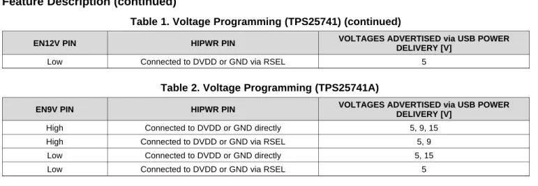
8.3.6 Configuring Voltage Capabilities (HIPWR, EN9V, EN12V)
The voltages advertised to USB Power Delivery-capable sinks can be configured to one of four different sets. The EN12V, or EN9V pin is not envisioned to be changed dynamically in the system, so changing its state does not trigger sending source capabilities. However, the TPS25741 or TPS25741A checks the status of the pin each time before it sends a source capabilities message using USB Power Delivery. Note that changing the state of the PCTRL pin forces capabilities to be re-transmitted. The device reads the HIPWR pin after a reset and latches the result.
Table 1. Voltage Programming (TPS25741)
EN12V PIN HIPWR PIN VOLTAGES ADVERTISED via USB POWER
DELIVERY [V]
High Connected to DVDD or GND directly 5, 12, 20
High Connected to DVDD or GND via RSEL 5, 12
Feature Description (continued)
Table 1. Voltage Programming (TPS25741) (continued)
EN12V PIN HIPWR PIN VOLTAGES ADVERTISED via USB POWERDELIVERY [V]
Low Connected to DVDD or GND via RSEL 5
Table 2. Voltage Programming (TPS25741A)
EN9V PIN HIPWR PIN VOLTAGES ADVERTISED via USB POWER
DELIVERY [V]
High Connected to DVDD or GND directly 5, 9, 15
High Connected to DVDD or GND via RSEL 5, 9
Low Connected to DVDD or GND directly 5, 15
Low Connected to DVDD or GND via RSEL 5
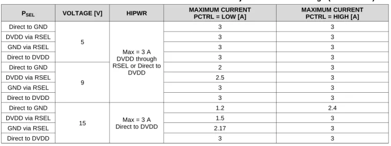
8.3.7 Configuring Power Capabilities (PSEL, PCTRL, HIPWR)
The power advertised to non-Power Delivery Type-C Sinks is always 15 W. However, the TPS25741 or TPS25741A only advertises Type-C default current until it debounces the Sink attachment for tCcDeb and the VBUS voltage has been given tVPto stabilize.
The device does not communicate with the cable to determine its capabilities. Therefore, unless the device is in a system with a USB Type-C plug and a cable built to support 5 A, the HIPWR pin should be used to limit the advertised current to 3 A.
PCTRL is an input pin used to control how much of the maximum allowed power the port will advertise. This pin may be changed dynamically in the system and the device automatically updates any existing USB Power Delivery contract. If the PCTRL pin is pulled below VPCTRL_TH, then the source capabilities offers half of the
maximum power specified by the PSEL pin.
The devices read the PSEL and HIPWR pins after a reset and latches the result, but the PCTRL pin is read dynamically by the device and if its state changes new capabilities are calculated and then transmitted.
While USB Power Delivery allows a maximum power of 100 W, the TPS25741 only advertises up to 93 W, which allows margin to ensure the output power remains below 100 W.
The PSEL pin offers four possible maximum power settings, but the devices can actually advertise more power settings depending upon the state of the HIPWR and PCTRL pins.Table 3summarizes the four maximum power settings that are available via PSEL, again note this is not necessarily the maximum power that is advertised.
Table 3. PSEL Configurations
MAXIMUM POWER (PSEL) [W]
PSEL
PSEL= 36 Direct to GND
PSEL= 45 DVDD via RSEL
PSEL= 65 GND via RSEL
PSEL= 93 Direct to DVDD
The following list provides a quick reference which applies to both TPS25741 and TPS25741A to see how the HIPWR, PSEL, and PCTRL pins affect what current is advertised with each voltage in the source capabilities message:
• If the PCTRL pin is low, then Pmax = PSEL/2
• If the PCTRL pin is high, then Pmax = PSEL. • If the HIPWR pin is pulled high, then Imax = 3 A. • If the HIPWR pin is pulled low, then Imax = 5 A. • For a voltage Vx, the advertised current is Ix
Table 4 and Table 5 provide a comprehensive list of the currents and voltages that are advertised for each voltage.
Table 4. Maximum Current Advertised in the Power Data Object for a Given Voltage (TPS25741)
PSEL VOLTAGE [V] HIPWR MAXIMUM CURRENTPCTRL = LOW [A] MAXIMUM CURRENTPCTRL = HIGH [A]
Direct to GND 5 Max = 3 A DVDD through RSEL or Direct to DVDD 3 3 DVDD via RSEL 3 3 GND via RSEL 3 3 Direct to DVDD 3 3 Direct to GND 12 1.5 3 DVDD via RSEL 1.87 3 GND via RSEL 2.7 3 Direct to DVDD 3 3 Direct to GND 20 Max = 3 A Direct to DVDD 0.9 1.8 DVDD via RSEL 1.12 2.24 GND via RSEL 1.62 3 Direct to DVDD 2.32 3 Direct to GND 5 Max = 5 A GND through RSEL or Direct to GND 3.6 5 DVDD via RSEL 4.5 5 GND via RSEL 5 5 Direct to DVDD 5 5 Direct to GND 12 1.5 3 DVDD via RSEL 1.87 3.74 GND via RSEL 2.7 5 Direct to DVDD 4.16 5 Direct to GND 20 Direct to GNDMax = 5 A 0.9 1.8 DVDD via RSEL 1.12 2.24 GND via RSEL 1.62 3.24 Direct to DVDD 2.32 4.64
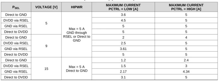
Table 5. Maximum Current Advertised in the Power Data Object for a Given Voltage (TPS25741A)
PSEL VOLTAGE [V] HIPWR MAXIMUM CURRENTPCTRL = LOW [A] MAXIMUM CURRENTPCTRL = HIGH [A]
Direct to GND 5 Max = 3 A DVDD through RSEL or Direct to DVDD 3 3 DVDD via RSEL 3 3 GND via RSEL 3 3 Direct to DVDD 3 3 Direct to GND 9 2 3 DVDD via RSEL 2.5 3 GND via RSEL 3 3 Direct to DVDD 3 3 Direct to GND 15 Max = 3 A Direct to DVDD 1.2 2.4 DVDD via RSEL 1.5 3 GND via RSEL 2.17 3 Direct to DVDD 3 3
Gate Control
G D N S VBUS Power SupplyCharge
Pump
RGDNGOFF C SL EW R SLEW G D N G 10:Power
Management
Safety Turnoff See VGDNGON & IGDNGONCopyright © 2016, Texas Instruments Incorporated
Table 5. Maximum Current Advertised in the Power Data Object for a Given Voltage (TPS25741A) (continued)
PSEL VOLTAGE [V] HIPWR MAXIMUM CURRENTPCTRL = LOW [A] MAXIMUM CURRENTPCTRL = HIGH [A]
Direct to GND 5 Max = 5 A GND through RSEL or Direct to GND 3.6 5 DVDD via RSEL 4.5 5 GND via RSEL 5 5 Direct to DVDD 5 5 Direct to GND 9 2 4 DVDD via RSEL 2.5 5 GND via RSEL 3.61 5 Direct to DVDD 5 5 Direct to GND 15 Max = 5 A Direct to GND 1.2 2.4 DVDD via RSEL 1.5 3 GND via RSEL 2.17 4.34 Direct to DVDD 3.1 5 8.3.8 Gate Drivers 8.3.8.1 GDNG, GDNS
The GDNG and GDNS pins may control a single NFET or back-to-back NFETs in a common-source configuration. The GDNS is used to sense the voltage so that the voltage differential between the pins is maintained.
VBUS Power Supply G D P G
Power
Management
RPPU CPPUI
GDPG CSLPCopyright © 2016, Texas Instruments Incorporated
Gate Control
VBUS Power SupplyCharge
Pump
RG5VOFF G 5 VPower
Management
Safety Turnoff See VG5VON & IG5VONCopyright © 2016, Texas Instruments Incorporated 8.3.8.2 G5V
The G5V pin may control an external NFET when the TPS25741/TPS25741A is used in a power multiplexor configuration, where one of two voltage inputs is connected to the VBUS pin. When G5V is not used to control an NFET, then it can be used to indicate if VBUS is being sourced at 5 V or not.
Figure 35. G5V Gate Control
8.3.8.3 GDPG
The GDPG pin may control an external PFET (single or back-to-back) when the TPS25741/TPS25741A is used in a power multiplexor configuration, where one of two voltage inputs is connected to the VBUS pin. When not used to control a PFET, this pin may be used to indicate when VBUS is being sourced at more than 5 V.
V BU S VBUS Deglitch tFOVPDG VFOVP GDNG Control Sampled every 1ms VSOVP Sampled every 1ms VSUVP Digital Control Digital Control
8.3.9 Fault Monitoring and Protection
8.3.9.1 Over/Under Voltage (VBUS)
The TPS25741 or TPS25741A uses the VBUS pin to monitor for overvoltage or undervoltage conditions and implement the fast-OVP, slow-OVP, and slow-UVP features.
Figure 37. Voltage Monitoring Circuits
If an over-voltage condition is sensed by the Fast OVP mechanism, GDNG is disabled within tFOVP+ tFOVPDG,
then a Hard Reset is transmitted and the VBUS discharge sequence is started. At power up the voltage trip point is set to VVFOVP (5 V contract). When a contract is negotiated the trip point is set to the corresponding VFOVP
value.
The devices employ another slow over-voltage protection mechanism as well that sends the Hard Reset before disabling the external NFET. It catches many OV events before the Fast OVP mechanism. During intentional positive voltage transitions, this mechanism is disabled (seeFigure 1). However, tVPafter the external NFET has been enabled if the voltage on the VBUS pin exceeds VSOVP, a Hard Reset is transmitted to the Sink then the
VBUS discharge sequence is started. Once a Power Delivery contract has been negotiated, if the voltage on the VBUS pin exceeds the selected voltage threshold (VSOVP) a Hard Reset is transmitted to the Sink then the VBUS
discharge sequence is started.
The devices employ a slow under-voltage protection mechanism as well that sends the Hard Reset before disabling GDNG. During intentional negative voltage transitions, this mechanism is disabled (see Figure 1). However, tVPafter the external NFET has been enabled if the voltage on the VBUS pin falls below VSUVP, a Hard
Reset is transmitted to the Sink then the VBUS discharge sequence is started..
8.3.9.2 Over-Current Protection (ISNS, VBUS)
OCP protection is enabled tVPafter the voltage on the VBUS pin has exceeded VBUS_RTH, seeFigure 38. Prior to OCP being enabled, the GD pin can be used to protect against a short.
The OCP protection circuit monitors the differential voltage across an external sense resistor to detect when the current outflow exceeds VITRIP which in turn activates an over-current circuit breaker and disables the GDNG /
GDNS gate driver. Once the OCP is enabled, if the voltage on the VBUS pin falls below VBUS_FTHthen that is also treated like an OCP event.
Following the recommended implementation of a 5 mΩ sense resistor, when the device is configured to deliver 3 A (via HIPWR pin), the OCP threshold lies between 3.8 A and 4.5 A. When configured to deliver 5 A (via HIPWR pin), the OCP threshold lies between 5.8 A and 6.8 A. The sense resistor may be increased to tighten the OCP threshold.
G D Deglitch tGDoff GDNG Control VGD_TH RG D VGDC
Copyright © 2016, Texas Instruments Incorporated
IS N S V BU S VBUS Power Supply Deglitch tOCP 5m: VITRIP GDNG Control VBUS_TH OCP Control Logic
Copyright © 2016, Texas Instruments Incorporated
Figure 38. Overcurrent Protection Circuit
8.3.9.3 System Fault Input (GD, VPWR)
The gate-driver disable pin provides a method of overriding the internal control of GDNG and GDNS. A falling edge on GD disables the gate driver within tGDoff. If GD is held low after a sink is attached for 600 ms then a hard
reset will be generated and the device sends a hard reset and goes through its startup process again.
The GD input can be controlled by a voltage or current source. An internal voltage clamp is provided to limit the input voltage in current source applications. The clamp can safely conduct up to 80 µA and will remain high impedance up to VGDCbefore clamping.
Figure 39. Overcurrent Protection Circuit
If the VPWR pin remains below its falling UVLO threshold (VPWR_TH) for more than 600 ms after a sink is
attached then the devices consider it a fault and will not enable GDNG. If the VPWR pin is between the rising and falling UVLO threshold, the TPS25741/TPS25741A may enable GDNG and proceed with normal operations. However, after GDNG is enabled, if the VBUS pin does not rise above its UVLO within 190 ms the devices consider it a fast-shutdown fault and disables GDNG. Therefore, in order to ensure USB Type-C compliance and normal operation, the VPWR pin must be above its rising UVLO threshold (VPWR_TH) within 275 ms of when UFP
is pulled low and the VBUS pin must be above VBUS_RTHwithin 190 ms of GDNG being enabled.
8.3.10 Voltage Control (CTL1, CTL2)
CTL1 and CTL2 are open-drain output pins used to control an external power supply as summarized inTable 6. Depending upon the voltage requested by the sink, the device sets the CTL pins accordingly. No current flows into the pin in its high-z state.