Title
A study of absorption coefficient spectra in a-Si : H films near the
transition from amorphous to crystalline phase measured by
resonant photothermal bending spectroscopy( 本文(Fulltext) )
Author(s)
YOSHIDA, Norimitsu; SHIMIZU, Yasuko; HONDA, Takashi;
YOKOI, Toshiaki; NONOMURA, Shuichi
Citation
[Journal of Non-Crystalline Solids] vol.[354] no.[19-25] p.[2164]
-[2166]
Issue Date
2008-05-01
Rights
Version
著者最終稿 (author final version) postprint
URL
http://hdl.handle.net/20.500.12099/26401
A study of absorption coefficient spectra in aSi:H films
near the transition from amorphous to crystalline phase
measured by resonant photothermal bending spectroscopy
Norimitsu Yoshida*, Yasuko Shimizu, Takashi Honda, Toshiaki Yokoi and Shuichi Nonomura *Environmental and Renewable Energy Systems Division, Graduate School of Engineering, National University Corporation GIFU UNIVERSITY, Yanagido 11, Gifu 5011193, JAPAN TEL & FAX: +81582932683, EMail: nyoshi@gifuu.ac.jp Abstract Optical absorption spectra of a widegap hydrogenated amorphous silicon film have been estimated by resonant photothermal bending spectroscopy. It is found that excess absorption existsover the photon energy region of 1.2 1.6 eV. This excess absorption decreases by light
illumination and does not recover through thermal annealing. The decrease in the excess absorption
may be due to oxidization of the film by light illumination.
PACS: 71.23.Cq, 78.55.Qr Manuscript
Introduction
Hydrogenated amorphous silicon (aSi:H) thin films deposited near the transition from
the amorphous to crystalline phase (widegap aSi:H) [1,2] is a promising material for the intrinsic
layer of the top cell in tandemtype solar cells. By application of such a material as the intrinsic
layer in solar cells, weaker photodegradation and higher open circuit voltages could be realized [2].
However, to the authors’ knowledge, optical absorption spectra from visible to near infrared region
of such a material have not yet been reported. Further, investigations of the relation between
photodegradation [3] and optical properties of the material seems to be important from the view
point of basic research as well as device applications.
We have previously suggested that resonant photothermal bending spectroscopy
(resonantPBS) [4,5] is a useful tool for evaluating optical absorption spectra of thin film
semiconductors. In this study, we have tried to apply this technique to widegap aSi:H [1,2] for the
first time for estimating absorption coefficient spectra !. Further, photoinduced effects on ! have
been also investigated by this technique.
Experimental procedures
Si thin films were prepared by the hotwire CVD method with deposition conditions
including substrate temperature of 300 oC, filament temperature of 1700 oC and SiH4 gas pressure
of 5 Pa. These are one set of deposition conditions in our apparatus used for preparing Si thin films
to be about 1.9 eV by a Tauc plot. The thickness of the film was 0.55 "m. For measurements of
optical absorption spectra, quartz glass plates with dimensions of 2 x 20 mm2 and a thickness of 0.1
mm were employed as substrates, which means that the sample has a bimorph structure like a
bimetal. For measurements of electrical conductivities, quartz glass plates with dimensions of 7 x
20 mm2 and a thickness of 0.5 mm were also employed as substrates.
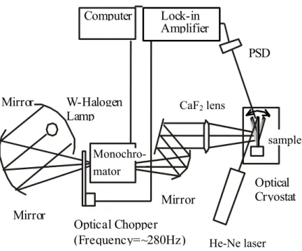
Figure 1 shows a schematic illustration of the experimental setup for the resonantPBS
system. This technique is a kind of photothermal spectroscopy, such as photoacoustic spectroscopy
(PAS) and photothermal deflection spectroscopy (PDS) [6]. In brief [4,5], when light illuminates a
bimorph sample constructed from a thin film semiconductor and a quartz glass substrate, a bending
occurs in the sample because of thermal expansion of the film due to nonradiative recombination
of photoexcited carriers. The magnitude of the bending is proportional to optical absorbance of the
film. Thus, we can estimate absorption spectra ! of thin film semiconductors.
A tungstenhalogen lamp was used as the visible and near infrared light source. The
monochromatic light illuminated the sample with a chopping frequency of about 280 Hz, which is
the resonant frequency of the sample itself. The bending of the sample, induced by the optical
absorption, was detected by the optical lever method as a displacement of a probe beam (HeNe
laser). The probe beam illuminates the sample’s free end and a position sensitive detector (PSD)
was employed for detecting the displacement of the reflected probe beam. The sample was kept in a
vacuum of about 101 Pa during the resonantPBS measurement using a specially designed optical
The absorption coefficient ! (cm1) [4,5] of the film at a photon energy of h"##is derived from
!(h") $%1
d
ln1% S(h")
S
sat&#
'#
(#
)#
*#
+#
(1)Here, S(h") is a PBS signal and Ssatis the value in the saturated region. d is a thickness of the
sample. The absorption coefficient !!(cm1) can be determined directly from Eq. (1) and was
confirmed by fitting to the absorption coefficient obtained by the analysis of optical transmittance
measurements.
For experiments on the photodegradation, a solar simulator with an intensity of 100
mW/cm2 and A.M.1.5 was employed as a light source. The light illumination was performed in air at room temperature. Al coplanar electrodes were prepared on the Si thin film by the conventional thermal evaporation method. The gap distance and the width were 60 "m and 3 mm, respectively. Results Optical absorption spectra of an aSi:H film with a wide bandgap energy of about 1.9 eV are shown in Fig. 2 by the solid line with solid circles. Those of a conventional aSi:H film with a bandgap energy of 1.75 eV and for a microcrystalline Si film [4,5] are also indicated by dashed and solid lines, respectively. It is found that there exists extra absorption with interference fringes at 1.2
~ 1.6 eV in the widegap aSi:H film, an absorption coefficient !# being about 102 cm1 at a photon
hydrogenated microcrystalline Si ("cSi:H) films.
Photoinduced effects in the widegap aSi:H film were investigated. The film was
illuminated in air at room temperature for 1 h with an intensity of 100 mW/cm2 (AM1.5). It was
observed that absorption coefficients at 1.2 1.6 eV decrease under light illumination as shown in
Fig. 3. For example, an absorption coefficient ! at a photon energy of 1.3 eV decreases from about
102 cm1 to 101 cm1. It is noted that a similar phenomenon was observed in the "cSi:H film (not
shown) with low crystallinity (about 30 %) and thus this photoinduced change in absorption spectra
seems to occur in films with amorphous structure. It should also be noted that this photoinduced
change in absorption coefficient spectra was not recovered by thermal annealing of the sample at
200 oC for 1 h in a vacuum of about 101 Pa (not shown). That is, the decrease of absorption
coefficient ! by light illumination is an irreversible phenomenon with respect to thermal annealing.
On the other hand, little photodegradation of the electrical conductivity was observed in this sample,
the photoconductivity being 1.1 x 10⁷ S/cm (not shown).
Discusssion
It is known that absorption coefficients below the bandgap energy region in conventional
aSi:H increase due to light illumination, as detected by PDS [6,7]. This phenomenon is usually
interpreted in terms of an increase of dangling bond density in the film by light illumination. One
possible explanation for the decrease of absorption coefficient in widegap aSi:H shown in Fig. 3 is
excess absorption at 1.2 1.6 eV in the widegap aSi:H film as shown in Fig. 2 may be diminished
through oxidization. Further, this interpretation could explain the irreversibility of the phenomenon
with respect to thermal annealing.
However, at present, the origin of the excess absorption in widegap aSi:H film is not
clear. Further investigations on absorption coefficient spectra and its photoinduced effects,
especially employing doped widegap aSi:H films, may clarify the energy level of the center
causing the excess absorption in the material.
Conclusion
We have demonstrated optical absorption spectra of an aSi:H film near the transition
from the amorphous to the microcrystalline phase and its photoinduced change by resonantPBS
technique for the first time. It is found that there exists excess absorption at a photon energy region
of 1.2 – 1.6 eV compared with those of a conventional aSi:H film. Further, this absorption found to
decrease by light illumination. The decrease of absorption may be explained by oxidization of the
film under light illumination.
Acknowledgements
This work was partly supported by NEDO (The Investigation for Innovative PV
Technology of METI), the Japan Science and Technology Agency (JST) and Electric Power
References [1] D. V. Tsu, B. S. Chao, S. R. Ovshinsky, S. Guha, J. Yang, Appl. Phys. Lett. 71 (1997) 1317. [2] J. Koh, H. Fujiwara, R. W. Collins, Y. Lee, C. R. Wronski, J. NonCryst. Solids 227230 (1998) 73. [3] D. L. Staebler and C. R. Wronski, Appl. Phys. Lett. 31 (1977) 292. [4] T. Kunii, K. Mori, J. Kitao, N. Yoshida, S. Nonomura, Rev. Sci. Instrum. 74 (2003) 881. [5] T. Kunii, N. Yoshida, Y. Hori, S. Nonomura, Jpn. J. Appl. Phys. 45 (2006) 3913. [6] N. M. Amer and W. B. Jackson, Semiconductors and Semimetals, (Academic, Orlands, 1984), Vol.21 B, p.88. [7] N. Souffi, M. Daouahi, L. Chahed, K. Zellama, P. Roca i Cabarrocas, Solid State Commun. 122 (2002) 259.
Figure captions
Figure 1 A schematic illustration of the experimental setup for resonantPBS [4,5].
Figure 2 Optical absorption spectra of an aSi:H film with a wide bandgap energy of about 1.9
eV (solid line with solid circles). Results for conventional aSi:H with a bandgap energy of 1.75 eV
and for a microcrystalline Si film are also shown by dashed and solid lines, respectively. The
experimental errors of all data are within the solid circle in the figure.
Figure 3 Photoinduced effect on the excess absorption for the widegap aSi:H shown in Fig. 2.
Solid and open circles indicate results before and after illumination of the sample. The experimental
Figure 1 N. Yoshida et al.
PSD
Mirro
r
Mirro
r
Mirror
Computer
WHalogen
Lamp
Optical
Cryostat
Lockin
Amplifier
Optical Chopper
(Frequency=~280Hz)
CaF2 lens HeNe laser sample Monochro matorFigure 2 N. Yoshida et al.
10
110
210
310
410
51 1.2 1.4 1.6 1.8 2 2.2 2.4
photon energy h
"
(eV)
ab
so
rp
tio
n
co
ef
fi
ci
en
t
!
(
cm
1)
widegap aSi:H conventional aSi:H "cSi:H !Figure 3 N. Yoshida et al.