INVITED PAPER Special Section on Recent Progress in Antennas and Propagation in Conjunction with Main Topics of ISAP2016
Half-Height-Pin Gap Waveguide Technology and Its Applications in High Gain Planar Array Antennas at Millimeter Wave Frequency ∗
Jian YANG†a),Member, Fangfang FAN††, Parastoo TAGHIKHANI†,andAbbas VOSOOGH†,Nonmembers
SUMMARY This paper presents a new form of gap waveguide technol- ogy – the half-height-pin gap waveguide. The gap waveguide technology is a new transmission line technology introduced recently, which makes use of the stopband of wave propagation created by a pair of parallel plates, one PEC (perfect electric conductor) and one PMC (perfect magnetic con- ductor), with an air gap in between less than a quarter of the wavelength at operation frequency. Applying this PEC/PMC gap plate structure to ridged waveguides, rectangular hollow waveguides and microstrip lines, we can have the ridged gap waveguides, groove gap waveguides and inverted gap waveguide microstrip lines, respectively, without requiring a conductive or galvanic contact between the upper PEC and the lower PMC plates. This contactless property of the gap waveguide technology relaxes significantly the manufacturing requirements for devices and antennas at millimeter wave frequencies. PMC material does not exist in nature, and an artificial PMC boundary can be made by such as periodic pin array with the pin length about a quarter wavelength. However, the quarter-wavelength pins, referred to as the full-height pins, are often too long for manufacturing. In order to overcome this difficulty, a new half-height-pin gap waveguide is introduced.
The working principles and Q factors for the half-height-pin gap waveguides are described, analyzed and verified with measurements in this paper. It is concluded that half-height-pin gap waveguides have similar Q factors and operation bandwidth to the full-height-pin gap waveguides. As an example of the applications, a high gain planar array antenna at V band by using the half-height-pin gap waveguide has been designed and is presented in the paper with a good reflection coefficient and high aperture efficiency.
key words: gap waveguide, half-height pins, Q factor, planar slot array, 60 GHz band
1. Introduction
Communication systems and other systems, such as sensors, radars and imaging, at millimeter wave (mmW) are necessary and important in nowadays societies in many perspectives.
MMW antenna systems including components and circuitry challenge us in twofold: the loss becomes unacceptable by using conventional transmission line technologies for large systems and the manufacture becomes difficult and costly due to the reduced size and the high tolerance requirements.
Facing these challenges, a new transmission line technology, the so-called gap waveguide, was proposed for mmW and THz applications by Prof. Kildal[1]a few years ago. High-
Manuscript received February 15, 2017.
Manuscript revised June 15, 2017.
Manuscript publicized August 22, 2017.
†The authors are with the Dept. Electrical Engineering, Chalmers University of Technology, Sweden.
††The author is with the Key Laboratory of Microwaves and Antennas, Xidian University, China.
∗This paper is a significant extension to one part of a paper presented at ISAP 2016.
a) E-mail: [email protected] (Corresponding author) DOI: 10.1587/transcom.2017ISI0002
gain mmW planar array antennas and components, such as power dividers, filters, couplers, have been developed by using this technology with high performances[2]–[7].
The gap waveguide technology makes use of the wave- stop phenomena between a PEC (perfect electric conductor) plate (realized by a metal plate) and a PMC (perfect mag- netic conductor) plate (realized by a pin structured metal plate) with an air gap in between less than quarter wave- length, and wave guidance along a waveguide form, such as ridges in ridged gap waveguides[8], microstrip lines in inverted microstrip line gap waveguides[9]and grooves in groove gap waveguides[10]. In gap waveguide technology electromagnetic waves are always prorogating in an air-filled guide structure. Therefore, the dielectric losses are avoided in the gap waveguide technology, which provides a solution to reducing the losses in mmW systems.
The fact that the two plates in gap waveguides are sepa- rate with an air gap in between avoids the use of any method of soldering, wielding, bonding or gluing. Then, many cost effective manufacture technologies can be used in mmW de- vices and systems with gap waveguide technology. Molding, milling, die forming, electrical discharge machining (EDM), microelectromechanical systems (MEMS) and 3D printing are some examples. However, pins in the previously de- veloped gap waveguide devices are always about quarter- wavelength long, a bit too long and thin at mmWs for manu- facturing, and poses a difficulty for low-cost manufacture. In order to overcome this difficulty in manufacture, a new pin form gap waveguide, the half-height-pin gap waveguide, has been proposed recently [11],[12]with the same electrical performance.
The purpose of this paper is to briefly describe the working principle of the half-height-pin gap waveguide, then analyze its Q factor and present a design example of 60 GHz high-gain planar antenna with this technology. The paper is organized as follows. In Sect. 2 we describe the basic working principle. In Sect. 3 the Q factor of ridged and groove gap waveguides with half-high pins are analyzed and verified with measurements. In Sect. 4 an example of 60 GHz planar array antenna is presented with the overall geometry and performance by simulations and measurements. Then, the paper is ended with conclusions.
2. Working Principle
A general structure of a periodic half-height unit pin is shown in Fig. 1(a). The working principle for the wave stop be- Copyright © 2018 The Institute of Electronics, Information and Communication Engineers
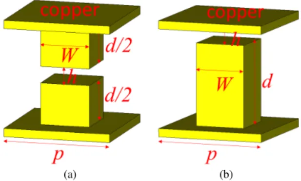
Fig. 1 Periodic unit pin structures for gap waveguide technology: (a) a half-height pin; (b) a full-height pin.
Fig. 2 Equivalent circuit (upper figure) of a single pin (lower figure) in an infinite periodical pin array modelled in CST. The front and back faces in red in the lower left figure are defined as ports 1 and 2, and the two side faces in blue in the lower right figure are defined as PMC walls in order to model the infinite periodic pin array. Note that the port faces and PMC faces are represented by half transparent faces.
tween a PEC plate and a PMC plate, realized by a periodic full-height (quarter wavelength) pin structure as shown in Fig. 1(b), does not hold for the half-height-pin structure. We need to use the analysis model for periodic structures pre- sented in[13]to define the working principle. The equivalent circuit to describe this structure is shown in Fig. 2, where the admittance ofj Bis determined by the periodic unit pin cell in the lower part of Fig. 2. The periodicity of the unit cell is defined by the two PMC planes in blue at the side faces of the CST modelled unit pin structure in the lower right part of Fig. 2. In an infinite cascaded two-port network the voltagesVn,Vn+1and currentsIn,In+1on thenth unit cell as shown in the figure are related with aABC Dmatrix as:
"
Vn In
#
=
"
A B C D
# "
Vn+1 In+1
#
. (1)
From [13], all wave propagations are stopped in the pin structure when
|A+D|>2. (2)
As an example, a half-height pin unit structure with p=1.71 mm,d =1.31 mm,w=0.79 mm andh=0.26 mm has been modeled in CST with PMC planes on the side faces and ports 1 and 2 on the front and back faces, as shown in
120 0.2
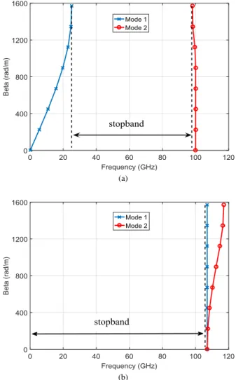
Fig. 2. The simulated ABCD matrix of the unit structure can be obtained from CST. Table 1 shows the simulated data of |A+D|. From the table, we can see that a stop band covers 43–110 GHz. As a verification, the same structure has been also full-wave simulated by using the Eigenmode solver in CST, and the stopband is from 43.3 to 106.5 GHz.
The physical explanation for the stop band is that the periodic structure is built up in such a way that the reflection from each cascaded unit cell has a constructive accumulation (make the reflection larger and larger after each cell) and propagation a destructive accumulation (make the propagation attenuated) over a certain frequency band. By using this model, we can also have an indication on the wave propagation attenuation:
the higher value of|A+D|, the higher attenuation of the wave propagation, which can help us to determine how many rows of pins are needed in practice.
The gaphbetween the pins has strong influence on the stop bandwidth. Figure 3 shows the dispersion diagrams for two cases: the gaph=0.1mmand zero gaph=0 mm with other dimensions defined in Table 2. It can be concluded with many simulation cases that the smaller gap, the wider the stop bandwidth, and zero gap is the best theoretically.
However, due to the imperfect flatness of the manufactured plates, it is very difficult to have zero gap for all pins with good contact in practice. The avoidance of the good contact requirement credits the gap waveguide technology over other conventional technologies. Therefore, a small gap such as 0.1 mm is preferred in practice.
3. Q Factor
Losses, including ohmic loss and radiation loss, are a critical factor for antenna and other systems at mmW. A good mea- sure of the losses for a certain transmission-line technology is the Q factor of a resonant cavity made by the technol- ogy. A high Q factor of a resonator is critical for designing a high-performance filter. In this Section, half-height-pin double-ridged/groove gap waveguide resonators have been numerically analyzed and compared with the full-height-pin counterparts at 60 GHz. It is known that it is not easy to have Q factor measured accurately for a resonator at mmW since all transitions and probes for measurements will introduce significant ohmic loss. Therefore, the analysis of Q factors in this work was carried out by only numerical simulations.
For measurement verification of the losses of half-height-pin gap waveguides, we choose to analyze the insertion loss of a piece of a half-height-pin double-ridged gap waveguide by both simulations and measurements.
Fig. 3 Effect of the gap heighthon stop bandwidth with (a)h=0.1 mm and (b) zero gaph =0 mm. The other pin’s dimensions are defined in Table 2.
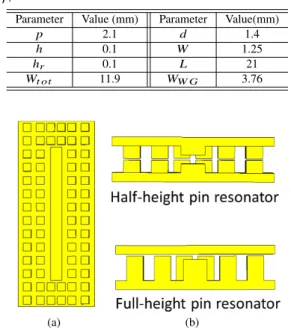
Table 2 Resonator’s dimensions with variedhrfor relation betweenQ andhr.
Parameter Value (mm) Parameter Value(mm)
p 2.1 d 1.4
h 0.1 W 1.25
Wr 1.8 L 21
Wt ot 11.9 WW G 3.76
3.1 Estimation of Ohmic Loss in Gap Waveguide
In order to analyze the simulated Q-factor in the work, we need to estimate the ohmic loss in a gap waveguide. As shown in Fig. 4, we assume that the ohmic loss in a gap waveguide comes mainly from the loss on ridges because no waves can propagate in the periodic pin part and the guided wave can propagate only along the ridge part. This assump- tion is accurate enough even for groove gap waveguide when the ridge gap heighthr, not the pin’s gaph, is the same as the height of waveguide. Assuming that the surface impedance of the ridge in a unit length of gap waveguide isZ =R+j X,
Fig. 4 Surface current on the ridges and surface impedance in gap waveg- uides: (a) a half-height-pin gap waveguide; (b) a full-height-pin gap wave- guide.
Fig. 5 Relationship between the longitudinal current densityJy on the ridge and the gap heighthrbetween the double ridges at 60 GHz with the structure in Fig. 3(a) modelled by copper of conductivity ofσ=5.8×10⁷ S/m.
and the surface current density on the ridge isJ=Jxxˆ+Jyy,ˆ as defined in Fig. 4, we have the ohmic lossPohmicper unit length of the gap waveguide due to the finite conductivityσ of the metal material used as
Pohmic≈2R Z Wr/2
−Wr/2|Jy|2dx=2RWr|Jy|2. (3) The factor of 2 is from the fact that the loss is from the top and the bottom ridges. Here we assume that the longitudinal current is much larger than the transverse currentJy Jx, andJis constant overxon the ridge. There is a resemblance between ridge/groove Gap waveguides and ridge/rectangular hollow waveguides[14]. Therefore, we can use Eqs. (11) and (12) in[15]to plot out the relationship between Jy andhr
andWr at 60 GHz by the blue lines in Figs. 5 and 6. The gap waveguide dimensions are listed in Table 2 and Table 3, modelled by copper with conductivity ofσ=5.8×10⁷S/m.
Jyh0 is the Jy when hr = 0.1 mm with other dimensions defined in Table 2 and JyW0 is the Jy whenWr =0.2 mm with other dimensions defined in Table 3. The function of (hr0/hr)0.71and(Wr0/Wr)0.82are fitting curves withhr0 = 0.1 mm andWr0 =0.2 mm.
BecauseQ∝1/Pohmic, from (3) and Figs. 5 and 6 we have an approximate relationship betweenQandhrandWr as
Fig. 6 Relation between the longitudinal current densityJyon the ridge and the gap widthWrbetween the double ridges at 60 GHz with the structure in Fig. 3(a) modelled by copper of conductivity ofσ=5.8×10⁷S/m.
Table 3 Resonator’s dimensions with variedWrfor relation betweenQ andWr.
Parameter Value (mm) Parameter Value(mm)
p 2.1 d 1.4
h 0.1 W 1.25
hr 0.1 L 21
Wt ot 11.9 WW G 3.76
Fig. 7 Resonator model: (a) the top view for both half-height pins and full-height pins; (b) the cross section of the resonators.
Q∝h0.71r , Q∝ 1
Wr0.18. (4)
3.2 Resonator Model for Q Factor Analysis
A double-ridged gap waveguide resonator with half-height pins is modeled by copper with conductivity ofσ=5.8×10⁷ S/m in Ansys HFSS Eigenmode solver for Q-factor analysis, shown in Fig. 7. As a reference for comparison, a full-height- pin ridged waveguide resonator is modeled as well, shown also in Fig. 7, with the same material and dimensions except for the pin height ofd and a single ridged waveguide. All dimensions are defined in Figs. 1, 4 and 7 with the values listed in Tables 2 and 3. The stopband of the pin struc- ture with the dimension values as in Table 2 is shown in
Fig. 8 Attenuation with two rows of pins verified by the simulated mutual coupling between two ridged half-height-pin gap waveguides separated with two rows of pins. The upper plate is not shown here for clarifying the structure.
Fig. 3(a), from 26 GHz to 100 GHz. We use this pin dimen- sions in the resonator with two rows on each side of the ridged gap waveguide, which is sufficient to stop the wave leakage through the air gap. This statement has been verified with a simulation of the mutual coupling below−40 dB at 60 GHz between two half-height-pin ridge gap waveguides separated by only two rows of pins shown in Fig. 8. The length of whole resonator is L =22.25 mm (10 pins along the short-circuit ridge), which corresponds to 4 wavelength (8-order resonator) at 53.93 GHz. In the end of the ridge two extra columns of pins are added to stop the wave leak- age and therefore make a resonator. The air gaphr between the double ridges will vary for analysis. When the air gap hr =d+h=1.5 mm in our case the ridge height is zero (the air gap is the same as waveguide height), the double-ridged gap waveguide becomes a groove gap waveguide.
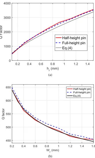
Figure 9(a) shows the simulated Q factors for both the half-height-pin and full-height-pin ridge gap waveguide res- onators with the air gap hr varying from 0.1 to 1.5 mm (a groove gap waveguide when hr = 1.5 mm), and the fit- ting curve by Eq. (4). The first observation is that the half- height-pin resonator has the almost identical Q factor as the full-height-pin resonator. Therefore, all previously devel- oped gap waveguide filters can be easily implemented by the half-height-pin double-ridged gap waveguide with the same performance. Secondly, the Q factor increases with the in- crease of the gap heighthr. This is because the higher gap height leads to the lower current density on the ridges, as shown in Fig. 5, and therefore, the lower ohmic loss on the ridges and the higher Q factor. Thirdly, the Q factor values can be predicted by (4) quite well.
Figure 9(b) shows the simulated Q factors of both the half-height and the full-height pin resonators when the ridge width is changed from 0.2 mm to 1.6 mm with other dimen- sions defined in Table 3. In the same figure, the calculated Q factor by (4) is also presented. It can be observed that the Q factor values decreases with the increase of the width of the ridges. This is because that although the current density
Fig. 9 Calculated and simulated Q factors of the resonators in Fig. 7 with (a) varied ridge gap heighthrand (b) varied ridge widthWr.
on ridges is reduced when the ridge width is increased, as shown in Fig. 6, the ohmic loss is still increased considering that the whole effect of the width isWr ·Wr−0.82=Wr0.18. The half-height-pin gap waveguide resonator has the similar Q factors as the full-height-pin one, and can be predicted by (4) quite well.
We have manufactured a prototype set of half-height- pin gap waveguides including a TRL calibration kit and a long waveguide, as shown in Fig. 10. The dimensions of the gap waveguides are defined as in Table 2 withhr =0.118 mm because we used a gap-waveguide-to-coplanar-waveguide transition in order to use GSG probe for the wideband mea- surement, where the substrate of the coplanar waveguide has 0.118 mm thickness. The measurement setup is shown in Fig. 11, with GSG probes. For details of design of the gap- waveguide-to-coplanar-waveguide transition, please refer to [16]. Figure 12 shows the simulated and measured (up to 67 GHz due to facility limitation) results, which agree with each other.
Fig. 10 Prototype set for measuring the insertion loss of a half-height- pin gap waveguide: (a) calibration kit and (b) a piece of long ridged gap waveguide. Note that the top plates are not shown here.
Fig. 11 Measurement setup.
Fig. 12 Simulated and measured insertion loss of the half-height-pine ridge gap waveguide.
4. Example of High Gain V-Band Planar Array An- tenna
An 8×8 planar slot array antenna based on the half-height- pin gap waveguide technology for 60 GHz[17]is presented here as an example of the applications of the technology. The corporate feeding network is designed by using ridge gap- waveguide with half-height pins. The distribution network is built up with the bottom plate and the middle plate, and
Fig. 13 Geometry of the 8×8 planar array antenna using the half-height- pin gap waveguide technology. Note that the bottom layer is made with such thickness only for connecting with standard flange where the positioning pins are 4 mm long.
Fig. 14 Photo of the prototype of the 8×8 V-band planar array antenna.
Fig. 15 Simulated and measured reflection coefficient of the 8×8 array antenna.
half-height pins are located on both the middle plate and the bottom plate but the ridge locates only in the bottom plate.
The cavity layer is built up on the top plate and the middle plate, and the half-height pins are located on both plates, as shown in Fig. 13.
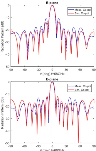
Figure 14 shows the prototype of the 8×8 V-band planar array antenna. Figure 15 shows the simulated and measured reflection coefficient of the prototype. It can be seen that
Fig. 16 Simulated and measured radiation patterns in E-plane over 58–
68 GHz.
there is a frequency shift about 2 GHz for this performance.
After measuring the dimensions of the prototype, we found that the main manufacture errors are the length of the pins.
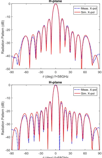
Many pins are shorter than the designed values with about 0.05 mm. Simulation with all pins 0.05 mm shorter indicates this shift, as shown in Fig. 15. High tolerance on pins’ length will be emphasized in future. Figures 16 and 17 shows the simulated and measured radiation patterns in E- and H- planes, respectively. The agreement between the simulation and the measurement is good. Figure 18 shows the simulated and the measured antenna gains, where the IEEE gain is the gain where the reflection loss is not included (but the ohmic loss is included) and the realized gain include all losses (reflection loss and ohmic loss). We see that the high reflection coefficient between 58 and 61 GHz affect the realized gain a lot, which we need to improve by better design and better manufacture.
5. Conclusions
This paper presents a new gap waveguide form - the half- height-pin gap waveguide for relaxing the manufacture re- quirements. The half-height-pin waveguide has the similar stop bandwidth and Q factor as the full-height-pin gap wave-
Fig. 17 Simulated and measured radiation patterns in H-plane over 58–
68 GHz.
Fig. 18 Simulated and measured antenna gain of the 8×8 array antenna, where dashed lines present different aperture efficiency levels ofea p = 60%,70% and 80%.
guide. One preliminary application of this new technology - a V-band 8×8 slot array antenna has be presented to show the potential of the technology.
Acknowledgments
During this work, the authors had a lot of discussions with Prof. Per-Simon Kildal and got advices from him. His sud- den decease is a big loss for us and we would like to contribute this work as a memory of his invention of the gap waveguide technology.
This project was funded by ERC Advanced Grant ERC- 2012-ADG-20120216 (PI: Prof. Kildal) and Fan’s visit to Chalmers University of Technology was supported by the Natural Science Foundation of China (NSFC) under Grant 61301068, the Fundamental Research Funds for the Central Universities (JB150207).
References
[1] P.-S. Kildal, E. Alfonso, A. Valero-Nogueira, and E. Rajo-Iglesias,
“Local metamaterial-based waveguides in gaps between parallel metal plates,” IEEE Antennas Wireless Propag. Lett., vol.8, pp.84–
87, 2009.
[2] E.A. Alos, A.U. Zaman, and P. Kildal, “Ka-band gap waveguide coupled-resonator filter for radio link diplexer application,” IEEE Trans. Compon., Packag. Manufact. Technol., vol.3, no.5, pp.870–
879, 2013.
[3] A.U. Zaman, P.-S. Kildal, and A. Kishk, “Narrow-band microwave filter using high-Q groove gap waveguide resonators with manufac- turing flexibility and no sidewalls,” IEEE Trans. Compon., Packag.
Manufact. Technol., vol.2, no.11, pp.1882–1889, 2012.
[4] A. Berenguer, M. Baquero-Escudero, D. Sanchez-Escuderos, B.
Bernardo-Clemente, and V.E. Boria-Esbert, “Low insertion loss 61 GHz narrow-band filter implemented with groove gap waveg- uides,” 44th European Microwave Conference (EuMC), pp.191–194, 2014.
[5] H. Raza, J. Yang, P.-S. Kildal, and E. Alfonso Alos, “Microstrip-ridge gap waveguide–study of losses, bends, and transition to WR–15,”
IEEE Trans. Microw. Theory Techn., vol.62, no.9, pp.1943–1952, 2014.
[6] H. Raza and J. Yang, “Compact UWB power divider packaged by using gap-waveguide technology,” 2012 6th European Conference on Antennas and Propagation (EUCAP), pp.2938–2942, 2012.
[7] J. Yang and H. Raza, “Empirical formulas for designing gap- waveguide hybrid ring coupler,” Microw. Opt. Technol. Lett., vol.55, no.8, pp.1917–1920, 2013.
[8] P.-S. Kildal, A.U. Zaman, E. Rajo-Iglesias, E. Alfonso, and A.
Valero-Nogueira, “Design and experimental verification of ridge gap waveguide in bed of nails for parallel-plate mode suppression,” IET Microw. Antennas Propag., vol.5, no.3, pp.262–270, 2011.
[9] E. Pucci, A.U. Zaman, E. Rajo-Iglesias, and P.-S. Kildal, “New low loss inverted microstrip line using gap waveguide technology for slot antenna applications,” Proc. 5th European Conference on Antennas and Propagation (EUCAP), pp.979–982, 2011.
[10] E. Rajo-Iglesias and P.-S. Kildal, “Groove gap waveguide: A rect- angular waveguide between contactless metal plates enabled by parallel-plate cut-off,” 2010 Proc. Fourth European Conference on Antennas and Propagation (EuCAP), pp.1–4, 2010.
[11] J. Yang and F. Fan, “Waveguides and transmission lines in gaps between parallel conducting surfaces (half-height pins and double period pins in both surfaces),” European Patent Application EP- 15186666.2, Gapwaves AB Sweden, Sept. 2015.
[12] F. Fan, J. Yang, and P.-S. Kildal, “Half-height pins—A new pin form in gap waveguide for easy manufacturing,” 10th European Confer- ence on Antennas and Propagation (EuCAP), Davos, Switzerland, 2016.
[16] F. Fan, J. Yang, V. Vassilev, and A. Uz Zaman, “Bandwidth investi- gation on half-height pin in ridge gap waveguide,” submitted to IEEE Trans. Microwave Theory Techn., 2016.
[17] P. Taghikhani, J. Yang, and A. Vosoogh, “High gain V-band pla- nar array antenna using half-height pin gap waveguide,” 2017 11th European Conference on Antennas and Propagation (EUCAP2017), pp.2758–2761, Paris, March 2017.
Jian Yang received the B.Sc. degree in elec- trical engineering from the Nanjing University of Science and Technology, Nanjing, China, in 1982, the M.Sc. degree in electrical engineering from the Nanjing Research Center of Electronic Engineering, Nanjing, in 1985, and the Swedish Licentiate and Ph.D. degrees from Chalmers University of Technology, Gothenberg, Sweden, in 1998 and 2001, respectively. From 1985 to 1996, he was with the Nanjing Research Institute of Electronics Technology, Nanjing, China, as a Senior Engineer. From 1999 to 2005, he was with the Department of Elec- tromagnetics, Chalmers University of Technology, Gothenberg, Sweden, as a Research Engineer. During 2005 and 2006, he was with COMHAT AB as a Senior Engineer. From 2006 to 2010, he was an Assistant Professor, from 2010 to 2016, he was an Associate Professor, and since 2016 he has been a professor with the Department of Signals and Systems, Chalmers Univer- sity of Technology. His research interests include 60–140 GHz antennas, terahertz antennas, MIMO antennas, ultrawideband (UWB) antennas and UWB feeds for reflector antennas, UWB radar systems, UWB antennas in near-field sensing applications, hat-fed antennas, reflector antennas, radome design, and computational electromagnetics.
Fangfang Fan received the B.S. in electro- magnetic field and microwave technology from Xidian University, Xi’an, China, in 2003, and the M.S. degree with the same major from Uni- versity of Electronic Science and Technology of China, Chengdu, China, in 2006. In 2006, she joined the Science and Technology on Antenna and Microwave Laboratory in Xidian University as an assistant, where she was involved with de- signing ultra-wideband antennas, microstrip an- tennas applied in SATCOM and passive circuits.
In 2011, she got Ph.D. degree and then was promoted as associated profes- sor. During 2015 to 2016, she was with Chalmers University of Technology as a visiting researcher, and did the research about gap waveguide. She holds 8 granted patents and has authored or coauthored over 20 referred journal and conference papers. Her current research interests involve microwave and millimeter-wave gap waveguide technology, including antenna arrays, filters, couplers, SIW antenna and circuits, planar antennas and reflector and antenna array design in SATCOM. Dr. Fan has served as the reviewer for the IEEE ANTENNA WIRELESS PROPAGATION LETTERS AND Progress In Electromagnetics Research.
burg, Sweden as a Ph.D. student, where she works on multi-physics analysis for mm-wave communication systems. Her main interests are phased-arrays antennas, microwave circuits and multi-physics analysis, especially for 5G applications.
Abbas Vosoogh received the B.Sc. degree in electrical engineering from the University of Sistan and Baluchestan, Zahedan, and the M.Sc.
degree from K.N. Toosi University of Technol- ogy, Tehran, Iran. He is currently pursuing his Ph.D. degree with Chalmers University of Tech- nology, Gothenburg, Sweden. His current re- search interests include the development of gap waveguide technology for millimeter and sub- millimeter wave applications, microwave passive components, EBG, soft and hard surfaces and 60 GHz planar array antennas based on Gap technology.