INVITED PAPER
Special Section on Solid-State Circuit Design — Architecture, Circuit, Device and Design MethodologyDigital Calibration and Correction Methods for CMOS Analog-to-Digital Converters
Shiro DOSHO†a),Member
SUMMARY Along with the miniaturization of CMOS-LSIs, control methods for LSIs have been extensively developed. The most predominant method is to digitize observed values as early as possible and to use digi- tal control. Thus, many types of analog-to-digital converters (ADCs) have been developed such as temperature, time, delay, and frequency converters.
ADCs are the easiest circuits into which digital correction methods can be introduced because their outputs are digital. Various types of calibration method have been developed, which has markedly improved the figure of merits by alleviating margins for device variations. The above calibration and correction methods not only overcome a circuit’s weak points but also give us the chance to develop quite new circuit topologies and systems.
In this paper, several digital calibration and correction methods for major analog-to-digital converters are described, such as pipelined ADCs, delta- sigma ADCs, and successive approximation ADCs.
key words: analog circuits, Moore’s law, high performance, system LSIs, miniaturization, digital calibration, correction
1. Introduction
System LSIs have been developed as essential devices for communication, mechanical control and medical care. Such application fields are still expanding.
The fundamental index of system-LSI technologies is Moore’s law [1], which resulted in an amazing revolution- ary increase in the integration density of the LSI, becoming hundredfold larger during the past decade. Even the 22 nm CMOS process will be in practical use at an early date.
Now system LSIs are frequently used in sensing sys- tems, which makes them much closer to us. Unlike in pre- vious cases of dealing with video or audio signals, many recent system LSIs digitize analog signals output from sen- sors, such as temperature, acceleration, and angular velocity, and so on.
In previous CMOS processes such as the 0.25 or 0.5μm CMOS process, most sensor systems were composed of analog-rich circuits, because a digital cell is too large for complex digital sensors.
However, the situation drastically changed owing to the further development of CMOS processes. This means that we can use more digital circuits than old process to realize sensing systems.
Figure 1 shows such a situation, which shows the num- ber of digital transistors equivalent to the energy consump- tion of an ADC. These graphs are based on typical 2006
Manuscript received August 31, 2011.
Manuscript revised October 21, 2011.
†The author is with Digital Core Development Center, Pana- sonic Corporation, Moriguchi-shi, 570-8501 Japan.
a) E-mail: [email protected] DOI: 10.1587/transele.E95.C.421
Fig. 1 Number of transistor gates equivalent to power consumption of ADC [2].
ADC energy per conversion number. It is clear that the num- ber drastically increases as CMOS processes are miniatur- ized.
Therefore, in the present system LSIs, it is mainstream to digitize analog signals as early as possible, which allows us to use more advanced signal processing including non- linear processes using huge resources of digital gates. This approach encourages the development of various types of analog-to-digital converter collaborating with digital cali- brations and corrections. Finally, the performance of ADCs is markedly improved as compared with the performance several years ago.
In this paper, main techniques for calibrating or cor- recting ADCs are described. “Calibration” means a method of maximizing the performance and “Correction” means a method of one-to-one conversion for correct output codes.
In Sect. 2, recent major types of ADC are introduced. In Sects. 3 to 7, calibration techniques for such ADCs are shown.
2. Circuit Configurations of Recent ADCs
2.1 Classification
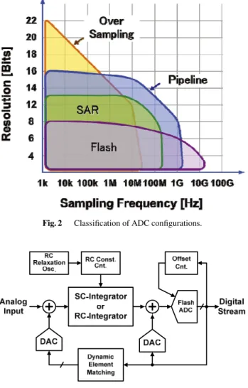
Figure 2 shows the classification of ADC configurations.
There are four main configurations of ADCs: oversampling, pipeline, successive approximation, and flash ADCs. Each configuration of ADC has a specific digital calibration tech- nique.
Copyright c2012 The Institute of Electronics, Information and Communication Engineers
Fig. 2 Classification of ADC configurations.
Fig. 3 Block diagram of oversampling ADC.
2.2 Oversampling ADCs
Figure 3 shows a block diagram of an oversampling ADC whose architecture is suitable for ADCs with a higher dy- namic range and a lower bandwidth less than 20 MHz [3]–
[5].
Those ADCs are a type of filter system for quantiza- tion noise using a feedback loop. As shown in Fig. 3, the ef- fect of the integrator pushes the quantization noise up to the high-frequency region so that the SNR in the low-frequency region becomes very high.
There are two means of realizing the integrator: one is to use a switched capacitor circuit and the other is to use a continuous time integrator. ADCs with the switched- capacitor (SC) integrator show stable operation and ease of changing the signal bandwidth at the cost of large power dis- sipation. In contrast, ADCs with the continuous-time (CT) integrator realize a higher bandwidth with a lower power dissipation. However, they are beset with a loop stability problem. In addition it is difficult for CT integrators to ad- just the signal bandwidth because the bandwidth depends on the absolute value of the RC constant.
Fig. 4 Block diagram of pipelined ADC.
In addition, it is essential for CT modulators to cal- ibrate the offset mismatch in flash ADCs and the current mismatch of each cell in the DAC for maximizing its signal to noise ratio.
2.3 Pipeline ADCs
Figure 4 shows a block diagram of the pipelined ADC con- sisting of cascaded pipe stages [6]. The pipe stage is a switched capacitor circuit with a low-resolution ADC.
The function of the pipe stage is to subtract a constant analog value from the input signal and to output the digital code corresponding to the value to be subtracted.
In actual implementation, the output residue of the pipe stage is amplified so that the dynamic ranges of all pipe stages are equal. It is the largest advantage of the pipeline ADC to introduce redundancy very easily, which makes the ADC insensitive to the offset of the comparator.
Thus, it is relatively easy to achieve ADCs with a res- olution higher than 12 bits using the above architecture. In addition, pipelined ADCs are suitable for high-speed oper- ation owing to the simplicity of each of the pipe stages [7].
Another important characteristic of this ADC is that the later the pipe stage is, the closer it is to the ideal operation of the pipe stage. This means that we can use later pipe stages for calibrating the earlier pipe stages that are more sensitive to the parasitic and mismatch of transistors.
Therefore, various calibration methods have been de- veloped to date [8].
2.4 SAR-Type ADCs
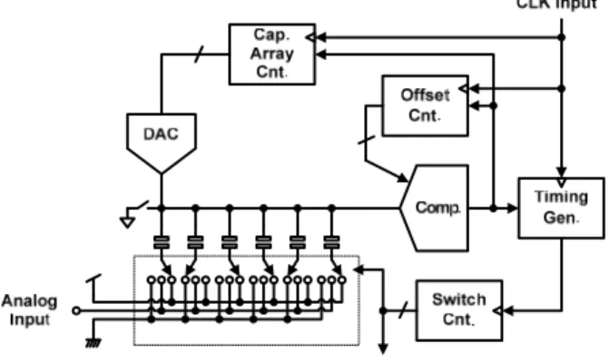
Figure 5 shows a block diagram of the successive approx- imation register (SAR) type ADC [9]. The architecture is very simple because the SAR requires no opamp, but only switches, capacitors and comparators. Thus, the SAR-type ADC is compatible with deep submicron CMOS processes.
First, an input voltage signal is stored in the plate on the comparator side of the capacitor array that is binary- weighted. Next, the binary search is conducted so that quan- tized voltage is applied to the opposite side of the capacitor array.
This type of ADC was invented in the early days of CMOS technologies. The architecture of the SAR has not changed for about 30 years. However, drastic improvement
has been carried out in recent years, because it has the po- tential to realize the lowest FOM among ADCs as long as the resolution of the ADC is less than 10 bits [10].
Multiple approaches to reducing the area of the capac- itor array, to operating asynchronously for high-speed oper- ation and to calibrating the mismatch of the capacitor array have been developed [11]. In a very recent paper, a 10 bit SAR with an FOM of 15.5 fJ/conv.-step in 100 MHz opera- tion has been reported [12].
2.5 Flash ADCs
Figure 6 shows a block diagram of the flash ADC. The ar- chitecture is the most basic, which outputs the thermometer code using comparators whose number is equal to the quan- tization levels of the ADC.
The flash ADC has the highest operating speed be- cause it requires no sample hold circuit. Sometimes, the input transistors of the comparator use the minimum gate length to enhance operating speed. Thus, an offset calibra- tion scheme is required [13]. In addition, trimming schemes for both clock timing and frequency characteristics of each comparator are also essential.
Aside from the ADC mentioned above, other archi-
Fig. 5 Block diagram of successive approximation register.
Fig. 6 Block diagram of flash ADC.
tectures exist: a dual-slope-type ADC for measurement hardware, a subranging ADC and an interpolated ADC [14]. However, the digital calibration schemes for the above ADCs are based on those for the four fundamental types of ADC. Here, we will not discuss the other types of ADC in- dividually.
3. Digital Calibration Scheme for ADCs
Figure 7 shows the fundamental calibration schemes for ADCs [15]. Figure 7(a) shows the oldest and the most gen- eral calibrating way. The system has two ADCs: an ADC to be calibrated and a high-accuracy and low-sampling-rate ADC for use as a reference. The same test signals are input into both ADCs and the differences between those outputs are stored in a table for calibration.
Although this method is applicable to most ADCs, the area of additional circuits becomes very large. Thus, it is a rare case to apply the method to practical use as it is.
Moreover, the error becomes larger when the frequency of the input signal becomes higher because the table is based on the data from the reference ADC with a low sampling rate.
A more efficient method is shown in Fig. 7(b), which uses an ADC with redundancy to generate calibration codes.
In general, an ADC with redundancy can generate two out- put codes of the ADC by switching the circuit configuration.
In an ideal case, the difference between the two codes should be zero. If the difference is not zero, it means that there is an error. Thus, the error can be used to calibrate the output code of the ADC.
The later method is the typical correction method for pipeline ADCs. Figure 7(b) shows a control block for changing the operation mode of the redundant path in an ADC. The table for calibration stores each error of the out-
Fig. 7 Fundamental calibration schemes for ADCs.
put codes corresponding to the switching modes of the re- dundant block of the ADC. The details of the calibration method of the pipeline ADC will be discussed later.
The increase in system size shown in Fig. 7(b) is much smaller than that shown in Fig. 7(a), because the correction table only stores errors whose number is equal to the number of the combination of redundant paths in the ADC.
However, note that we can use this method to calibrate the DNL only, because the method compensates for the con- tinuity of the output codes. It should depend on the other means to calibrate global characteristics such as INL.
4. Digital Calibration Methods for Pipelined ADCs In this section, we describe three major calibration methods:
DNL error calibration, calibration of the DNL in the back- ground, and calibration of the memory effect arising when we use a double-sampling architecture.
4.1 DNL Calibration Method
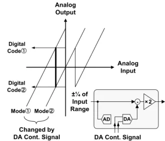
One of the distinguishing characteristics of the pipeline ADC is that we can calibrate earlier pipe stages using the output code from later pipe stages because the later the pipe stage is, the more the gain of the pipe stage relaxes the re- quired performance of itself. Figures 8(a) and 8(b) show the input-output characteristics of the 1- and 1.5-bit pipe stages, respectively.
Provided that the comparator has an offset voltage at its input, the output of the 1-bit pipe stage is outside of the dy- namic range, which makes it impossible to estimate the in- put value from the output code of the pipe stages connected after the stage for calibration. On the other hand, the 1.5-bit pipe stage tolerates a much larger offset of the comparator.
As long as the input offset is less than one-fourth of the input range, the output voltage is within the dynamic range [16].
In the pipeline ADC, each pipe stage subtracts the ana- log value, and the residue is amplified and sent to the suc- cessive pipe-stage. Each stage outputs a digital code corre- sponding to the analog value subtracted at the pipe stage.
Fig. 8 Input-output characteristics of pipe stage.
Thus, the most important thing is to find an accurate digital code corresponding to the actually subtracted analog value. That is to say, the question is how to determine the digital code. In Fig. 8(b), output digital codes corresponding to the operation modes of the pipe stage are shown along the x-axis. The subtracted analog values are the output differ- ences between the operation modes that are discontinuous changes at boundaries of the operation modes [thick line in Fig.(9)].
In an ideal case, the analog subtraction is half of the output range that is equal to the difference between the out- put digital codes, which is 1 in this case (00→01 or 01→10).
However, the nonideality of the pipe stage, such as the capacitance mismatch of the switched capacitor circuits or the finite gain of the amplifier breaks the assumption. Thus, we have to measure real digital codes corresponding to the subtracted analog values.
Figure 9 shows the method for determining the digi- tal code corresponding to the subtracted analog value. First, the input test signal is set to one-fourth of the input range, which is close to the boundary of the operation mode. Next, the DAC in the pipe stage is forced to be modes 1and 2 successively and each output code is measured in the fol- lowing pipe stages.
If the characteristics of the following pipe stages are ideal, the difference between digital codes 1and 2is the real digital value corresponding to the subtracted analog value [17]. Fortunately, this assumption works well, be- cause the later the pipe stage is, the more its nonidealities are suppressed by the gain of the stage.
Thus, we have to start the calibration at the most sub- sequent stage needed for calibration. When the calibration at the stage is finished, the stage seems to operate ideally.
Next, the calibration moves to the previous stage, and the calibration continues until the first pipe stage is cali- brated.
Fig. 9 Measurement method of determining digital code corresponding to subtracted analog value.
Fig. 10 Background calibration.
4.2 Calibration in Background
The calibration method mentioned in Sect. 4.1 requires a certain period to perform, which means that the A-to-D con- version has to be stopped in the period. Thus, several ways of calibration along with the A-to-D conversion have been developed in recent years.
These calibration methods are called “Background Cal- ibration”. A typical background calibration uses both redun- dancy and pseudo-random (PN) codes.
An outline of the background calibration is shown in Fig. 10 [18]. The input-output characteristics of the pipe- stage are slightly different from those in Fig. 8(b), which has two types of characteristic: one corresponds to the PN=0 (faint line) and the other corresponds to the PN=1 (black line). The probabilities of the pipe stages choosing each conversion characteristic converge to 50% after a sufficient period. Provided that the probability density distribution of the input signal is flat, the difference between two averages of the digital output for each conversion characteristic ex- presses the subtracted analog value. Thus, we can calibrate the pipe stage in the background.
4.3 Memory Effect Calibration in Double Sampling Pipeline ADC (DSPADC)
DSPADC is an interesting circuit configuration that real- izes high-speed and efficient operation. Figure 11 shows the block diagram and operation of the DSPADC.
The DSPADC includes two pipeline ADCs whose opamps are shared [19]. Thus, as shown in Fig. 11(b), one is in the sample hold operation and the other is in the settling operation. Only the settling operation requires an opamp.
Thus, an opamp can be shared by interleaving.
However, there is no period for resetting capacitors during the operation, resulting in the memory effect prob- lem. Here, the memory effect means that the residual charge in the settling period causes an error in the next settling pe- riod of the opposite pipe stage.
The effect becomes larger at a higher sampling speed, because DC gain tends to be lower in such a case.
The actual residual charge can be derived from the re- lationships shown in Fig. 12. The output voltage of the pipe stage is calculated as follows.
Fig. 11 Block diagram and operation of DSPADC.
Fig. 12 Block diagram and operation of DSPADC.
Vout =α·Vin±β·Vref +γ·Vout−1
= C s+C f
C f+C s+CfA+C p ·Vin± C s C f+C s+C fA+C p
·Vref+ C p
C s+(1+A)·C f +C p ·Vout−1 (1) In Eq. (1), theα,βandγare the output gain, the coef- ficient of the subtracted analog value and the coefficient of the memory effect, respectively. In the DSPADC, there are two sets ofβandγ, because it includes two pipeline ADCs.
Here, we use the following variables:βA,βB,γA, andγB. Thus, there are four variables for describing the outputs of the pipe stages. This means that we need four test patterns to derive these variables.
Figure 13 shows the four test patterns for deriving the coefficients of the memory effects. We measure four digital
Fig. 13 Test patterns for calculating coefficients of memory effect.
Fig. 14 Measurement result of DSPADC with memory effect calibration.
codes,EA,EA, EBandEB,shown in Fig. 13. These vari- ables correspond to the subtracted analog value of the pipe stage.
Finally, the following equations are used to derive the coefficients of the memory effect.
γA = EA−EA
EB+EB, γB= EB−EB
EA+EA (2)
Other variables,βAandβB, are derived simultaneously.
Instead of measuring the gain of the pipe stage,α, we mea- sure the total gain of the ADC, which is derived by the least- mean-square (LMS) method. Thus, we input four test sig- nals to the ADC. The slope of the output is approximated by the LMS method.
Figure 14 shows the measurement result of the DSPADC with the memory effect calibration. The test chip was fabricated in 40 nm CMOS; it includes a 10-bit DSPADC with an operating speed of 260 MHz. It is ob- vious that the errors caused by the memory effect shown in Fig. 14(a) disappear after the calibration, as shown in Fig. 14(b). In addition, the difference between the two pipeline ADC is sufficiently close for practical use.
5. Calibration Methods for Delta-Sigma ADCs
Delta-sigma ADCs are an oversampling ADCs which are a type of filter system whose quantization noise is localized in a high-frequency region owing to the filter effect. Thus a low-frequency signal has a very high signal to noise ratio (SNR).
Although delta-sigma ADCs have a potential to realize a high SNR, each block of these ADCs requires a very high linearity that cannot be realized in CMOS processes.
Fig. 15 Simulation results of modulator with large distortion DAC.
Thus, several techniques have been developed to relax the required linearity of each block in delta-sigma ADCs.
In this section, we introduce essential calibration meth- ods for delta-sigma ADCs.
5.1 Dynamic Element Matching
In delta-sigma ADCs, the block most sensitive to linearity of the output codes is the feedback DAC. The delta-sigma modulator is a feedback system, which means that the feed- back signal coincides with the input signal at an accuracy of 1/K [K is the DC gain of the K(ω)]. This is effective even if the feedback DAC has a large distortion.
Even if the DAC in Fig. 15 has a large distortion, the analog feedback signal (DAC output) has a small distortion due to the suppression by the large feedback gain. In con- trast, the digital codes (Quantizer output) have a large dis- tortion to compensate for the better linearity of the analog feedback signal. Therefore, the DAC linearity is one of the most important factors in achieving sufficient SNDR of the modulator.
The main factor of the nonlinearity of the DAC is the mismatches between current cells in the DAC. The most popular means of alleviating the mismatch in the DC is to convert it to high-frequency components. This is called as
“data-weighed averaging (DWA)” [20].
Figure 16 shows the block diagram of the DWA [21]. In the DWA, each DAC cell has its own address. The cells are selected in the next turn so that the next address starts from one plus the maximum address among the cells used at a given moment. If the maximum address at a given moment is n and the number of DAC cells used in the next turn is m, the address in the next turn is from n+1 to n+m. The encoder in Fig. 16 outputs the number of DAC cell used in the current turn and the accumulator outputs the address to be used in the next turn. The switch matrix rotates DAC cells so that the lowest comparator in Fig. 16 is connected to the DAC cell whose address is the first address to be used in the next turn.
Fig. 16 Block diagram of data-weighted averaging.
Fig. 17 Sources of 2nd-order distortion.
5.2 Suppression of 2nd-Harmonic Distortion
Although the DWA effectively alleviates the distortion caused by the mismatch effect of DAC cells, it generates a 2nd-order distortion when the opamp in the 1st integra- tor has an offset voltage. Figure 17 shows sources of the 2nd-order distortion. When the 1st integrator has an offset voltage ofΔV, this offset voltage interacts with the parasitic capacitances of the current source of the DAC cell,Cp and Cn, and generates a 2nd-order distortion.
The details of generating a 2nd-order distortion are given in Fig. 18. When the 1st integrator has an offset volt- age, DWA varies the charge stored in parasitic capacitances at the current source with a half-period of the input signal.
Thus a 2nd-order distortion is generated by the interaction.
Figure 19 validates the effect of the offset calibration using the test chip. The DWA and the offset calibration of the 1st integrator are applied to a 3rd-order delta-sigma modulator. A more than 10 dB SFDR improvement has re- sulted from the offset calibration of the 1st integrator. In this case, the means of calibration is to use an offset DAC for canceling the offset at the output of the input differential stage.
5.3 Calibration of RC Constant
In the case of continuous time delta-sigma modulators, aside
Fig. 18 Generation mechanism of 2nd-order distortion.
Fig. 19 Effect of the offset calibration for 2nd-order distortion.
from the DWA and offset calibration, the calibration of the RC constant of the integrator is essential, because the RC constant is an absolute value that varies too widely.
Figure 20 shows the circuit configuration of the RC re- laxation oscillator for RC constant calibration [22]. In the oscillator shown in Fig. 20, the threshold voltage of the com- parator is controlled by the feedback loop so that the integral of the oscillator output is constant. This control loop real- izes an ideal oscillator insensitive to PVT variation. The oscillation frequency of the oscillator is determined by the following equations.
(1−α) (TOS C/RC)=1−e−(TOS C/RC), ∴α=Vref
Vdd
(3) In Eq. (3), we can easily make a variableαconstant us- ing a resistor ladder. Thus, the oscillation frequency (Tosc) depends on only the RC constant. Thus, we can determine accurately the RC constant by measuring the oscillation pe- riod of the oscillator. Resistors in the modulator are changed
Fig. 20 RC Relaxation oscillator for RC constant calibration.
Fig. 21 Improvement in SNR by RC constant calibration.
so that the RC constant of the modulator can be set to the target value.
Figure 21 shows the measurement result of the im- provement in SNR by RC constant calibration. RC-constant calibration can improve the SNRs of all samples to more than 69.5 dB.
6. Calibration Methods for SAR-Type ADCs
The classification of the input-output characteristics of SAR is shown in Fig. 22. There are two cases: one in which the array capacitance of the upper bit is larger than twice that of the lower bit, and the other is the opposite of the first case.
In the former case, we can specify the analog input corre- sponding to the digital output code as shown in Fig. 22(a).
However, it is impossible to specify the analog input in the latter case as shown in Fig. 22(b), because plural analog in- puts correspond to one digital output.
Thus, the SAR is not suitable to be calibrated only in the digital domain. Some modifications of the analog parts are essential to realize an efficient and simple calibration of SARs.
Actually, a SAR using 1.86-bit coding instead of bi- nary coding was reported [23]. However, this circuit config- uration increases both the complexity and area of the SAR.
Moreover, it deteriorates the FOM of the SAR, which is
Fig. 22 Classification of in-out characteristics of SAR.
Fig. 23 Capacitor array DAC with redundancy.
originally very small by its nature.
Therefore, the most popular means of calibrating the SAR is to use an additional capacitive DAC, which is shown in Fig. 5. The calibration method using the DAC is very sim- ple. First, the offset of the comparator is calibrated to zero.
Then, the capacitance of the capacitor to be calibrated is compared with capacitance corresponding to all of the lower bits of the capacitor to be calibrated so that the two objects being compared are equal.
On the other hand, it is suitable to increase the sam- pling speed to introduce redundancy into a SAR. Figure 23 compares a capacitor array with and without a redundancy.
Figure 23(a) shows a capacitor array of 3bit configuration.
On the other hand, Fig. 23(b) shows an additional array for a 2nd bit with a 3-bit configuration to introduce redundancy.
The easiest way to explain redundancy is to draw a tree of bi- nary search. Figure 24 shows a comparison of binary search trees. Figure 24(a) shows the conventional type tree of DAC shown in Fig. 23(a), Fig. 24(b) corresponds to Fig. 23(b). In the conventional tree, if the comparator errs in the compar- ison, the output data never return the correct code. In con- trast, in the search tree in Fig. 23(b), the output data can return the correct code even if the comparator errs, because each of the six digital codes from the center have two search paths.
The drawback of introducing redundancy is the in- crease in the conversion period of one comparison cycle.
Fig. 24 Binary search tree of SAR.
However, the total period would be shorter than the con- ventional one because each redundancy allowing a larger settling error shortens the every comparison cycle. A 10- bit SAR with a 100 MHz operating clock has been reported [12].
7. Calibration Methods for Other ADCs
7.1 Delta-Sigma Modulator Using Open-Loop VCO In this section, we describe an outline of a recent new ADC that uses a time dimension [24].
Figure 25 shows a block diagram of the 1st-order delta- sigma ADC using a time dimension. The input analog volt- age is converted to timing information by the VCO. At this moment, input voltage is converted to the phase of the VCO, which means that the input signal is integrated. Then the phase information is quantized. Finally, the quantized phase is converted to frequency information by differentiation.
Thus, the quantization noise shifts to the high-frequency re- gion by differentiation. On the other hand, the input sig- nal that is digitized as frequency information is not affected by the frequency operations, because the signal is integrated and differentiated, the effects of which cancel out each other.
A dummy VCO is linearized by the feedback loop us- ing the LMS method. The main VCO is also linearized by the same information of the dummy loop. Thus, the main VCO is linearized within the relative accuracy of two VCOs.
When we apply the LMS to a high-order polynomial, we have to solve simultaneous equations. However, the imple- mentation of such solver in the LSI is not appropriate, be- cause it is complex and takes a large chip area.
A simpler means of solving high-order polynomials is to use the steepest descent method. For example, to approx- imate measured result as a third-order polynomial,y(x) = a0+a1x+a2x2+a3x3, the following recurrence formulas are used.
Fig. 25 Block diagram of the 1st-order delta-sigma modulator using VCO.
Fig. 26 Block diagram of steepest descent method for LMS.
⎧⎪⎪⎪⎪⎪⎪⎪
⎪⎪⎪⎪⎪
⎪⎪⎪⎨⎪⎪⎪⎪⎪
⎪⎪⎪⎪⎪
⎪⎪⎪⎪⎪
⎩
α(k0+1)=α(k)0 +2Δα m
m
i=1(ti−y(xi)) α(k1+1)=α(k)1 +2Δα
m m
i=1(ti−y(xi))x α(k2+1)=α(k)2 +2Δα
m m
i=1(ti−y(xi))x2 α(k3+1)=α(k)3 +2Δα
m m
i=1(ti−y(xi))x3
(4)
Here, m is the number of samples andΔa is the parameter for approximating speed and accuracy. Figure 26 concretizes the idea in Eq. (4). The steepest descent method gives us a simple circuit configuration and it is applicable to almost all circuits. However, we have to carefully consider the draw- back that it rarely falls into a local minimum point or that it cannot converge into the solution.
7.2 Remaining Issues and Notifications
Thus far, we have calibrated various analog characteristics using digital circuits. However, there are some issues that need to be solved in the future. One of these issues is cal- ibrating a time interleaving system. When we use an ADC with time interleaving, the high-frequency spurious effect falls into a signal band due to sampling skew. In addition, the variation in the frequency characteristics of each ADC causes harmonic distortions. Although some interesting ap- proaches have been reported, it would be difficult to put the
methods practical use owing to both size and power over- head issues [25], [26].
Another point to remember in using digital calibration is noise contamination during the calibration. Noise con- tamination sometimes deceives a calibration system. Thus, we have to avoid contamination during the calibration pe- riod.
8. Conclusions
In this paper, we briefly discussed calibration and correction methods for CMOS-ADCs. The performance of ADCs has been improved markedly by combining with digital collec- tion methods over the last decade. It is very interesting that some circuit configurations thought not to work at a glance are now put into the center stage by using the digital cali- bration. Thus, this fact will give ADC designers a chance to produce innovative circuits by the digital calibration. We hope for this exciting condition to continue as long as pos- sible.
Acknowledgment
The author would like to express his gratitude to the members of the Panasonic ADC design group, especially to Mr. K. Matsukawa, Dr. K. Obata, Mr. Y. Mitani, Mr. M. Takayama, Dr. Y. Tokunaga, Dr. T. Morie, Mr. S. Sakiyama and Mr. T. Miki for offering materials for the preparation of this paper. The author is also grateful to the Associate Editor and the anonymous reviewers for their constructive and valuable comments and suggestions for the improvement of the quality of this paper.
References
[1] G.E. Moore, “Cramming more components onto integrated circuits,”
Electron. Mag., pp.114–117, April 1965.
[2] B. Murmann, “Digitally assisted analog circuits,” IEEE Microw., vol.26, no.2, pp.38–47, March/April 2006.
[3] K. Matsukawa, Y. Mitani, M. Takayama, K. Obata, S. Dosho, and A.
Matsuzawa, “A 5th-order delta-sigma modulator with single-opamp resonator,” Symposium on VLSI Circuits, pp.68–69, June 2009.
[4] G. Mitteregger, C. Ebner, S. Mechnig, T. Blon, C. Holuigue, E.
Romani, A. Melodia, and V. Melini, “A 14b 20 mW 640 MHz CMOS CT ΔΣ ADC with 20 MHz signal bandwidth and 12b ENOB,” IEEE ISSCC, Dig. Tech. Papers, pp.131–140, Feb. 2006.
[5] P. Malla, H. Lakdawala, K. Kornegay, and K. Soumyanath, “A 28 mW spectrum-sensing reconfigurable 20 MHz 72 dB-SNR 70 dB- SNDR DTΔΣADC for 802.11n/WiMAX receivers,” IEEE ISSCC Dig. Tech. Papers, pp.496–497, Feb. 2008.
[6] S.H. Lewis and P.R. Gray, “A pipelined 5-M samples/s 9-bit analog- to-digital converter,” IEEE J. Solid-State Circuits, vol.SC-22, no.6, pp.954–961, Dec. 1987.
[7] K. Matsukawa, T. Morie, Y. Tokunaga, S. Sakiyama, Y. Mitani, M.
Takayama, T. Miki, A. Matsumoto, K. Obata, and S. Dosho, “Design methods for pipeline and delta-sigma A-to-D converters with convex optimization,” Proc. ASP-DAC, pp.690–695, Yokohama, Japan, Jan.
2009.
[8] H.-C. Liu, Z.-M. Lee, and J.-T. Wu, “A 15-b 40-MS/s CMOS pipelined analog-to-digital converter with digital background cali- bration,” IEEE J. Solid-State Circuits, vol.40, no.5, pp.1047–1056,
May 2005.
[9] J.L. McCreary and P.R. Gray, “All-MOS charge redistribution Analog-to-Digital conversion techniques — Part 1,” IEEE J. Solid- State Circuits, vol.SC-10, no.6, pp.371–379, Dec. 1975.
[10] M. Yoshioka, K. Ishikawa, T. Takayama, and S. Tsukamoto “A 10b 50 MS/s 820μW SAR ADC with on-chip digital calibration,” ISSCC Dig. Tech. Papers, pp.384–385, Feb. 2010.
[11] M. van Elzakker, E. van Tuijl, P. Geraedts, D. Schinkel, E.
Klumperink, and B. Nauta, “A 1.9μW 4.4 fJ/Conversion-step 10b 1 MS/s Charge-Redistribution ADC,” ISSCC Dig. Tech. Papers, pp.244–245, Feb. 2008.
[12] C.C. Liu, S.J. Chang, G.Y. Huang, Y.Z. Lin, C.M. Huang, C.H.
Huang, L. Bu, and C.C. Tsai, “A 10b 100 MS/s 1.13 mW SAR ADC with binary-scaled error compensation,” ISSCC Dig. Tech. Papers, pp.386–387, Feb. 2010.
[13] P. Uzzo, G. Van der Plas, F. De Bernardinis, L. van der Perre, B. gy- selinckx, and P. Terreni, “A 10.6 mW/0.8 pJ power-scalable 1 GS/s 4b ADC in 0.18μm CMOS with 5.8 GHz ERBW,” Proc. 43rd An- nual Design Automation Conference, pp.873–878, June 2006.
[14] Y. Asada, K. Yoshihara, T. Urano, M. Miyahara, and A. Matsuzawa,
“A 6 bit, 7 mW, 250 fJ, 700 MS/s Subranging ADC,” A-SSCC, 5-3, pp.141–144, Taiwan, Taipei, Nov. 2009.
[15] J. Ming and S.H. Lewis, “An 8-bit 80-Msample/s pipelined analog- to-digital converter with background calibration,” IEEE J. Solid- State Circuits, vol.36, no.10, pp.1489–1497, Oct. 2001.
[16] K. Gotoh and O. Kobayashi, “3 states logic controlled CMOS cyclic A/D converter,” IEEE Custom Integrated Circuits Conference, pp.366–369, Sept. 1986.
[17] Y.M. Lin, B. Kim, and P.R. Gray, “A 13-b 2.5-MHz Self-calibrated Pipelined A/D Converter in 3-μm CMOS,” IEEE J. Solid-State Cir- cuits, vol.26, no.4, pp.628–636, April 1991.
[18] H.C. Liu, Z.M. Lee, and J.T. Wu, “A 15 b 20 MS/s CMOS pipelined ADC with digital background calibration,” ISSCC Dig. Tech. Pa- pers, pp.454–539, Feb. 2004.
[19] K. Nagaraj, H.S. Fetterman, J. Anidjar, Stephen H. Lewis, and R.G.
Renninger, “A 250-mW, 8-b, 52-Msamples/s parallel-pipelined A/D converter with reduced number of amplifiers,” IEEE J. Solid-State Circuits, vol.32, no.3, pp.312–320, March 1997
[20] T.R. Baird and T.S. Fiez, “Linearity enhancement of multibitΔΣA/D and D/A converters using data weighted averaging,” IEEE Trans.
Circuits Syst. II, vol.42, no.12, pp.753–562, Dec. 1995.
[21] W. Yang, W. Yang, W. Schofield, H. Shibata, S. Korrapati, A.
Shaikh, N. Abaskharoun, and D. Ribner, “A 100 mW 10 MHz-BW CTΔΣmodulator with 87 dB DR and 91 dBc IMD,” ISSCC Dig. of Tech. Papers, pp.498–499, Feb. 2008.
[22] Y. Tokunaga, S. Sakiyama, A. Matsumoto, and S. Dosho, “An on- chip CMOS relaxation oscillator with power averaging feedback us- ing a reference proportional to supply voltage,” IEEE International Solid-State Circuit Conference, pp.404–405, Feb. 2009.
[23] W. Liu, P. Huangm, and Y. Chiu, “A 12b 22.5/45MS/s 3.0 mW 0.059 mm2CMOS SAR ADC achieving Over 90 dB SFDR,” ISSCC Dig. Tech. Papers, pp.380–381, Feb. 2010.
[24] G. Taylor and I. Galton, “A mostly digital variable-rate continuous- time ADCΔΣmodulator,” ISSCC Dig. Tech. Papers, pp.298–299, Feb. 2010.
[25] P. Nikaeen and B. Murmann, “Digital correction of dynamic track- and-hold errors providing SFDR>83 dB up to fin=470 MHz,” Proc.
IEEE Custom Integrated Circuits Conference, pp.161–164 Sept.
2008.
[26] C. Vogel, “A signal processing view on time-interleaved ADCs,”
in Analog Circuit Design, Chap.4, pp.61–78, Springer, 2010.
ISBN978-90-481-3082-5
Shiro Dosho was born in Toyama, Japan, in 1964. He received his M.S. and D.S. degrees from Tokyo Institute of Technology in 1989 and 2005, respectively. He joined the Semiconduc- tor Research Center of Matsushita Electric In- dustrial Co., Ltd. in 1989. He is a Hardware Design expert in Panasonic Digital Core Devel- opment Center. He has over 20 years of expe- rience developing various CMOS mixed-signal circuits, such as analog memories, CT-Filters, PLLs, delta-sigma modulators, and pipelined ADCs. He has 27 U.S. Patents for his research work. Since 2009, he has been a member of the program committee of the IEEE VLSI Circuit Sym- posium. He served as a guest Editor-in-Chief for special issues on analog LSI technology of IEICE Transactions on Electronics in 2011.