SUMMARY To realize three-dimensional (3D) optical interconnection on large-scale integration (LSI) circuits, layer-to-layer couplers based on Si-photonics platform were reviewed. In terms of optical cross talk, more than 1µm layer distance is required for 3D interconnection. To meet this requirement for the layer-to-layer optical coupler, we proposed two types of couplers: a pair of grating couplers with metal mirrors for multi-layer distance coupling and taper-type directional couplers for neighboring layer distance coupling. Both structures produced a high coupling efficiency with relatively compact (∼100µm) device sizes with a complementary metal oxide semiconductor (CMOS) compatible fabrication process.
key words: Si photonics, 3D optical interconnection, layer-to-layer cou- pler, grating
1. Introduction
Recent progress in computing technologies has gradually changed people’s daily lives, such as Internet of Things (IoT) and artificial intelligence (AI). These computing tech- nologies rely on high-end large-scale computing systems in super computers or data centers. To enhance computing speed, optical interconnections have recently become im- portant to ensure large enough I/O bandwidths, essential for parallel computing. Therefore, modern data centers have in- stalled optical interconnections between centers, racks, and boards. Furthermore, in state-of-the-art super computers, attempts have been made to install the optical interconnec- tion even inside the boards. Ultimately, optical intercon- nection on electrical large-scale integration (LSI) circuits should be the target to enhance computing speed. To realize such on-chip interconnections, we proposed semiconductor membrane InP-based photonic integrated circuits (PICs) and demonstrated low threshold and high efficiency lasers on an Si substrate[1]–[4].
We also proposed to integrate an amorphous-silicon (a- Si) layer on conventional crystalline-silicon (c-Si) to realize three-dimensional (3D) stacks[5]. In fact, recent electrical LSIs have multi (∼10) electrical wiring layers on a comple-
Manuscript received November 13, 2017.
Manuscript revised February 15, 2018.
∗This is a review article.
†The authors are with Tokyo Institute of Technology, Tokyo, 152–8550 Japan.
∗∗Presently, with the KIST, Seoul, 02792 Korea.
∗∗∗Presently, with the Santec Corp, Komaki-shi, 485–0802 Japan.
∗∗∗∗Presently, with the Sony Corp, Tokyo, 108–0075 Japan.
∗∗∗∗∗Presently, with the AIST, Tsukuba-shi, 305–8561 Japan.
a) E-mail: [email protected] DOI: 10.1587/transele.E101.C.501
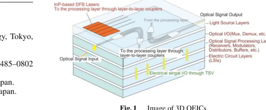
mentary metal oxide semiconductor (CMOS) layer. There- fore, we believed it was a natural progression to develop 3D stacks, even for PICs. Figure 1 shows the image of a 3D opto-electronic integrated-circuit (3D-OEIC) drawn in our internal proposal when we started the project 10 years ago.
Optical transaction, optical I/O, and light source layers (in the InP-based membrane PICs) were placed on the electrical transaction layers, including the CMOS transistors. Except for the top light source layer, all other layers consisted of Si or Si-based materials. If this type of OEIC chip could be realized, the signal transaction speed by one single chip, as well as parallel computing, would be significantly enhanced, since there would be essentially no limitation in the wiring bandwidth.
Moreover, this 3D stack technology can be used to re- duce the footprint of photonic modules, especially when multiplexing transmission systems, such as wavelength di- vision multiplexing (WDM), are used. Usually, the sizes of multiplexers or demultiplexers are large. If these large com- ponents can be stacked vertically the total size of the circuits can be reduced[6].
To realize these 3D stacks of photonic layers on CMOS circuits, process compatibility is very important. One way to ensure this compatibility is by using bonding methods after a separate fabrication process for each stacked wafer. An- other simple way is by direct stacks using deposition meth- ods. However, there is the limitation of process tempera- ture. Since the thermal tolerance of the CMOS layer is usu- ally less than 400◦C, we cannot deposit c-Si, which requires a much higher temperature, on the CMOS layer. In con- trast, the deposition temperature of a-Si is∼300◦C. There- fore, multiple stacking of photonic layers with an a-Si core is well suited for 3D optical interconnection. In Sect. 2, the
Fig. 1 Image of 3D OEICs.
Copyright c⃝2018 The Institute of Electronics, Information and Communication Engineers
Fig. 2 Optical crosstalk between two Si core layers after propagation in 100µm length waveguides as a function of layer distance[8].
basic characteristics of such a-Si stacking is described.
Coupling the signal between layers is also a critical is- sue to be solved for realizing 3D optical interconnection. If the interlayer thickness between the layers is relatively thin (<few hundred nm), a simple directional coupler type de- vice with linear taper structure is sufficient[7]. However, such small interlayer thickness produces unwanted signal crosstalk between layers. Our calculation shows the inter- layer thickness of cladding material (usually SiO2) between layers should be more than 1µm to suppress the crosstalk to less than−30 dB as shown in Fig. 2[8]To achieve signal coupling with a relatively thick interlayer thickness, several proposals were demonstrated[9], [10]. We proposed two types of couplers. The first is a grating-type coupler, that achieved several-µm distance coupling; e.g. from the 1st to the 3rdlayer coupling. The other is a directional coupler- type structure with double or curved-shape tapers for neigh- boring layer coupling. The characteristics of these couplers are reviewed in Sects. 3 and 4.
2. Basic Characteristics of a-Si:H Layer for 3D Stack
As mentioned in Sect. 1, a-Si is a core material for 3D stacks in optical interconnections. To reduce the material loss of the a-Si, we used a hydrogenated a-Si (a-Si:H) structure us- ing plasma enhanced chemical vapor deposition (PECVD).
The material gases were SiH4and Ar. The RF (13.56 MHz) power of the plasma was 100 W and the chamber pressure was 30 Pa. The chamber temperature was set to 300◦C.
For the 3D optical interconnection, the fabrication process was as follows: First, SiO2 was deposited by PECVD for the bottom cladding layer. Then, the a-Si:H layer with a thickness of 220 nm was deposited, under the aforemen- tioned conditions. The waveguide patterns were exposed by electron-beam lithography, followed by Si etching using CF4inductively-coupled-plasma reactive-ion-etching (ICP- RIE). Again, SiO2 was deposited as a cladding layer be- tween the core layers. However, after the deposition, the surface did not have a flat surface. Therefore, chemical me- chanical polishing (CMP) was carried out. After CMP, the
Fig. 3 Optical properties of a-Si:H.
surface roughness (root-mean-square: RMS) was ∼0.31–
0.39 nm. Then, another a-Si layer was deposited and the process continued until the desired number of layers was obtained. By introducing CMP process, the film quality of a-Si might be concerned since the film quality of a-Si is sensitive to the film condition of the underneath layer. To check this, we carried out ellipsometry measurements. Fig- ures 3(b) and 3(c) show the refractive index and absorption spectra of a-Si. The three lines in the figures correspond to the different samples, a-Si on the SiO2/Si substrate, a-Si on the SiO2/SOI substrate, and a-Si on the SiO2/a-Si/SiO2/Si substrate as shown in Fig. 3(a). For the latter two samples, CMP was carried out before the a-Si:H deposition. No dif- ference was observed in the material properties even after the CMP process. The material absorption at a wavelength of 1.55µm was negligible. Using this process, the transmis- sion loss of the Si-waveguides as a function of layer number was measured. The size of the Si-waveguide cores was 500
viewed. As mentioned in Sect. 1, the layer-to-layer distance should be at least 1µm. Changing the light propagation di- rection to upward/downward using a grating is an effective way to couple light over large distances. By introducing a pair of grating couplers, the light signal can move from one layer to another. Figures 4(a) and 4(b) show the im- ages of the grating-type layer-to-layer couplers. Two kinds of couplers were demonstrated. One had a pair of gratings (Fig. 4(a))[8],[11]. The other had a pair of gratings with metal mirrors at the bottom and top of the grating couplers (Fig. 4(b)][12],[13].
The fabrication process was essentially the same as that explained in Sect. 2. For the case with metal mirrors, the metallization process by electron-beam evaporation was also performed. In our experiment, gold was used for the mirror material due to equipment limitations. However, Aluminum is also suitable (almost same coupling perfor- mance can be achievable according to our calculation) and is commonly used in CMOS processes. To control the SiO2
thickness by CMP,ex-situthickness monitor measurements were used. Figure 5 shows a scanning electron microscope (SEM) image of the coupler with metal mirrors. The thick- ness targets for the mirror-to-Si core and core-to-core were
Fig. 4 Grating-type layer-to-layer couplers[8],[11]–[13].
the 1 layer was under the measurement limit. Without the metal mirror, the light from the grating radiated equally both upward and downward, and only half of the radiated power was captured. By introducing the metal mirrors, the down- ward radiated power was reflected. If the thickness between the mirror and the core coincided for the in-phase condition, the amount of upward optical power was enhanced. Figure 7 shows the intensity profiles of the upward radiated light of the grating for different thicknesses of the mirror and core DM. With a thickness of 800 nm, there was a threefold in- crease in the intensity compared with that without mirror.
Fig. 5 SEM image of the fabricated coupler[12].
Fig. 6 Transmittance spectra of the fabricated coupler. The red and blue points are the devices with and without metal mirrors, respectively[12].
Fig. 7 Calculated intensity profiles of the upward radiated light from the grating.zis the position along the waveguide light propagation direction.
The origin ofzis the position of the first grating trench.
Fig. 8 Eye diagram under 50 Gbps data transmission through the fabri- cated grating coupler with metal mirrors[12].
Fig. 9 Change in transmission distance with the coupling efficiency for uniform (blue) and apodized (red) gratings[14].
For a thickness of 1100 nm, the intensity decreased due to the out-of-phase condition. This parameter was most sen- sitive for coupling efficiency. Other parameters such as the alignment between the couplers had wider tolerance. De- tailed information about design and tolerance is in our pre- vious publication Ref.[13].
Figure 8 shows the eye diagram under 50 Gbps data transmission through the grating coupler with metal mirrors.
We could not observe any degradation after the transmis- sion. Although this grating coupler pair with uniform grat- ing duty ratio achieved a high coupling efficiency for a given thickness, it was strongly dependent on the transmission dis- tance, as shown in Fig. 9. This is because the profile of the radiated power was not symmetric and the profiles of the
Fig. 10 Calculated intensity profiles of radiated light fromS(z) andS’(z) of the bottom and top gratings, respectively. zis the position along the waveguide light propagation direction.
Fig. 11 Leakage factor at each position of the grating (red) and the cal- culated intensity profile from the designed apodized grating (blue).zis the position along the waveguide light propagation direction.
bottom and top gratings were not equal, as shown in Fig. 10 (the lines ofS(z) andS’(z) uniform). This can be solved by introducing apodization of the grating duty to control the leakage factor at each position of the grating. By adjusting the duty ratio at each position as shown in Fig. 11, the radi- ation intensity profile was tuned. After adjusting the profile, the radiation profiles of the bottom and top gratings were well matched as shown in Fig. 10 (the lines ofS(z) andS’(z) apodized), resulting in a coupling efficiency with almost no dependence on the transmission distance[14].
These results indicated several-µm transmission was possible using the apodized structure. Therefore, direct layer-to-layer coupling with jumping several layers can be possible.
4. Directional Coupler with Complex Taper Structure
If the signals transmit only to neighboring layers, a much simpler structure can be used; a directional coupler struc- ture with tapers. The layer-to-layer directional coupler with linear tapers were demonstrated with an interlayer thickness of 200 nm[7]. However, as mentioned before, at least 1 µm was needed to reduce unwanted crosstalk. By introduc-
Fig. 12 Schematic structure of a directional coupler with double taper.
Fig. 13 Optical mode field at the same position (120µm from the start point of the tapers) for conventional and double taper structures under same the taper length design.
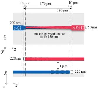
ing the linear taper structure for such a thickness, the length of the coupler becomes cm-order. In contrast, a double ta- per structure was proposed to reduce the length, as shown in Fig. 12[15]. The taper was divided into two sections.
One had a steep slope angle and the width of the waveguide was varied from 500 to 200 nm for c-Si and 250 nm for a- Si:H. In this section, the size of the optical mode was rapidly widened while maintaining an adiabatic coupling condition.
The other section had a moderate slope angle. Optical cou- pling occurred mainly in this section. Figure 13 shows the comparison of the optical mode field size at the same posi- tion for conventional linear and double taper structures. A larger field size was clearly observed for the double taper structure. For a total length of 190 µm, a coupling effi- ciency of 96% was achieved in the theoretical calculation for the TE-mode light. Figure 14 shows a SEM image of the fabricated double taper structure. The fabrication process was the same as the aforementioned description. Although a combination of c-Si and a-Si:H was used in this exper- iment, other combinations are possible, such as a-Si:H/
Fig. 14 SEM image of the center of the fabricated couplers with a double taper structure.
Fig. 15 Transmittance through the fabricated Si waveguides and cou- plers as a function of number of couplers. The Interlayer distance was
∼1µm.
a-Si:H and c-Si/InP membrane. The coupling efficiency was estimated using measurements of the transmittance of cou- plers by changing the number of couplers that light expe- riences. The TE-mode light was input to waveguides with different numbers of the couplers. The coupling efficiency was derived from the slope of the fitting curve of transmit- tance as a function of the number of couplers. A coupling efficiency of 0.59 dB/coupler (87%) was obtained from the results shown in Fig. 15. Please note the value contained the insertion loss of the coupler itself. This value was slightly lower than that of the theoretical calculation and the reason for this is the topic of future research. A similar structure could be also designed for the TM-mode. The alignment tolerance was much wider than the accuracy of conventional stepper (<50 nm) used in CMOS fabrication process. More detailed information about design and tolerance is in our previous publication Ref.[15].
For a further reduction of the coupler size, a directional coupler with curved taper structure was proposed[16]. Fig- ure 16 shows the structure of the proposed coupler. The shape of the tapers was determined by the function √t
z,
Fig. 16 Schematic structure of a directional coupler with curved ta- pers[16].
Fig. 17 Coupling efficiency for varioustvalues as a function of total taper length[16].
Fig. 18 Intensity profile of the coupler with a taper shape oft=7.
wherezis the position along waveguide propagation direc- tion andt is the order of the root. Iftequals 1, the shape is linear. Figure 17 shows the calculated coupling efficiency for various values oftas a function of total taper lengthL, with an interlayer thicknessDof 1 µm. Fortvalues of 7
or 10, a high coupling efficiency (98%) was achieved with taper lengths of 90 and 60µm, respectively. Please note the fabrication tolerance was low for the case oft = 10. To achieve>80% coupling, less than 40 and 20 nm accuracies were needed for the widths of the waveguide, for the cases oft=7 andt=10, respectively. Figure 18 shows the inten- sity profile along the propagation direction for the case of t=7. A smooth transition was observed without scattering or reflection. By introducing this structure, a 1/100 size re- duction was possible compared with the conventional linear taper structure for a 1-µm interlayer thickness.
5. Conclusion
Structure and characteristics of several types of layer-to- layer couplers were reviewed for 3D optical interconnec- tions on a Si-platform. A CMOS compatible fabrication process with low loss a-Si:H and chemical mechanical pol- ishing were used to produce the photonic layer stack with a relatively low transmission loss. For layer-to-layer couplers, a pair of grating couplers with metal mirrors for multi-layer jumping coupling and a directional coupler with taper struc- ture for the neighboring layer coupling were proposed. A coupling efficiency of>80% for the fabricated devices with interlayer thicknesses of 1µm was demonstrated. We be- lieve this technology shows great potential for the future of 3D high density optical interconnections.
Acknowledgments
The authors would like to thank Profs. S. Akiba, T.
Mizumoto, M. Asada, Y. Miyamoto, M. Watanabe, S.
Suzuki, and Y. Shoji of the Tokyo Institute of Technology for their fruitful discussions. This work was supported by JSPS KAKENHI (Grant Numbers #15H05763, #16H06082, and #17H03247); by the New Energy and Industrial Tech- nology Development Organization (NEDO).
References
[1] S. Arai, N. Nishiyama, T. Maruyama, and T. Okumura,
“GaInAsP/InP membrane lasers for optical interconnects,” IEEE J. Sel. Topics Quantum Electron., vol.17, no.5, pp.1381–1389, Sep./Oct. 2011. DOI: 10.1109/JSTQE.2011.2128859
[2] T. Hiratani, T. Shindo, K. Doi, Y. Atsuji, D. Inoue, T. Amemiya, N. Nishyama, and S. Arai., “Energy Cost Analysis of Membrane Distributed-Reflector Lasers for On-Chip Optical Interconnects,”
IEEE J. Sel. Topics Quantum Electron., vol.21, no.6, pp.1503410-1–
1503410-10, Nov./Dec. 2015. DOI: 10.1109/JSTQE.2015.2456334 [3] D. Inoue, T. Hiratani, K. Fukuda, T. Tomiyasu, Z. Gu, T. Amemiya,
N. Nishiyama, and S. Arai, “Integrated optical link on Si substrate using membrane distributed-feedback laser and p-i-n photodiode,”
IEEE J. Sel. Topics Quantum Electron., vol.23, no.6, pp.3700208- 1–3700208-8, July 2017. DOI: 10.1109/JSTQE.2017.2716184 [4] T. Hiratani, D. Inoue, T. Tomiyasu, K. Fukuda, T. Amemiya, N.
Nishiyama, and S. Arai, “High efficiency operation of membrane distributed-reflector lasers on silicon substrate,” IEEE J. Sel. Top- ics Quantum Electron., vol.23, no.6, pp.3700108-1–3700108-8, July 2017. DOI: 10.1109/JSTQE.2017.2704289
[5] J. Kang, Y. Atsumi, M. Oda, T. Amemiya, N. Nishiyama, and S.
[8] J. Kang, N. Nishiyama, Y. Atsumi, T. Amemiya, and S. Arai, “Multi- stacked silicon wire waveguides and couplers toward 3D optical in- terconnects,” Proc. SPIE, vol.8630, pp.863008–863012, 2013.
[9] J.T. Bessette and D. Ahn, “Vertically stacked microring waveguides for coupling between multiple photonic planes,” Optics Express, vol.21, pp.13580–13591, 2013. DOI:10.1364/OE.21.013580 [10] R. Takei, Y. Maegami, E. Omoda, Y. Sakakibara, M. Mori, and
T. Kamei, “Low-loss and low wavelength-dependence vertical in- terlayer transition for 3D silicon photonics,” Opt. Express, vol.23, no.14, pp.18602–18610, 2015. DOI:10.1364/OE.23.018602 [11] J. Kang, Y. Atsumi, M. Oda, T. Amemiya, N. Nishiyama, and
S. Arai, “Layer-to-Layer Grating Coupler based on Hydrogenated Amorphous Silicon (a-Si:H) for 3D Optical Circuits,” Jpn. J. Appl.
Phys., vol.51, no.12, pp.120203-1–120203-3, Nov. 2012. DOI:
10.1143/JJAP.51.120203
[12] J. Kang, Y. Atsumi, Y. Hayashi, J. Suzuki, Y. Kuno, T. Amemiya, N.
Nishiyama, and S. Arai, “50 Gbps data transmission through amor- phous silicon interlayer grating couplers with metal mirrors,” Appl.
Phys. Express, vol.7, no.3, pp.032202-1–032202-3, Feb. 2014. DOI:
10.7567/APEX.7.032202
[13] J. Kang, Y. Atsumi, Y. Hayashi, J. Suzuki, Y. Kuno, T. Amemiya, N. Nishiyama, and S. Arai, “Amorphous-Silicon Inter-Layer Grat- ing Couplers with Metal Mirrors toward 3D Interconnection,” J. Sel.
Top. Quantum Electron., vol.20, no.4, pp.8202308-1–8202308-6, July-Aug. 2014. DOI: 10.1109/JSTQE.2014.2300058
[14] Y. Kuno, J. Kang, Y. Hayashi, J. Suzuki, T. Amemiya, N. Nishiyama, and S. Arai, “Design of apodized hydrogenated amorphous silicon grating couplers with metal mirrors for inter-layer signal coupling:
Toward three-dimensional optical interconnection,” Japanese J. Ap- plied Physics, vol.54, no.4S, pp.04DG04-1–04DG04-6, June 2014.
DOI: 10.7567/JJAP.54.04DG04
[15] K. Itoh, Y. Hayashi, J. Suzuki, T. Amemiya, N. Nishiyama, and S.
Arai, “Double Taper Interlayer Transition Coupler for 3D Optical Interconnection with Heterogeneous Material Stacking,” The 48th Solid State Devices and Materials (SSDM 2016), no.C-1-02, Sept.
2016.
[16] K. Itoh, N. Nishiyama, Y. Hayashi, J. Suzuki, T. Amemiya, and S.
Arai, “Design of curved taper interlayer coupler for multilayered photonic integrated circuits,” 2017 autumn JSAP annual meeting, 6a-C13-7, Sept. 2017 (in Japanese).
wavelength InP-based VCSELs. Since 2006, he has been an Associate Professor with the Tokyo Institute of Technology. His current main inter- ests include transistor lasers, silicon photonics, III–V silicon hybrid op- tical devices, and terahertz–optical signal conversions involving optics–
electronics–radio integration circuits. Dr. Nishiyama is a member of the Japan Society of Applied Physics (JSAP), IEEE and IEICE. He was the recipient of the Excellent Paper Award from the Institute of Electronics, Information and Communication Engineers (IEICE) of Japan in 2001, the Young Scientists’ Prize of the Commendation for Science and Technology from the Minister of Education, Culture, Sports, Science and Technology in 2009, and the Ichimura Prize in Science for Distinguished Achievement in 2016.
JoonHyun Kang was born in Seoul, Korea, in 1986. He received the B.E., M.E., and Ph.D.
degrees in Electrical and Electronic Engineering from the Tokyo Institute of Technology, Japan, in 2010, 2012 and 2014, respectively. He is cur- rently working at the Nanophotonics Research Center, Korea Institute of Science and Technol- ogy. His current research interests are the devel- opment of semiconductor lasers and their appli- cations.
Yuki Kuno was born in Ibaraki Prefecture, Japan, in 1991. He received the B.E. and M.E.
degrees in Electrical and Electronic Engineering from the Tokyo Institute of Technology, Japan, in 2014 and 2016, respectively. During his M.E.
work, he focused on 3D optical integrated cir- cuits, especially for apodized grating couplers.
He is currently working in Santec Corp, Japan.
Kazuto Itoh was born in Tokyo, Japan, in 1991. He received the B.E. and M.E. de- grees in Electrical and Electronic Engineering from the Tokyo Institute of Technology, Japan, in 2015. During his M.E. work, he focused on c- Si/a-Si:H mixed optical circuits. He is currently working in Sony, Japan.
Yuki Atsumi received the B.E., M.E., and Ph.D. degrees in Electrical and Electronic Engineering from Tokyo Institute of Technol- ogy, Japan, in 2009, 2011, and 2013, respec- tively. During his Ph.D. work, he demonstrated athermal photonic integrated devices on a sil- icon platform incorporating Benzocyclobutene (BCB) polymer. He joined the National Institute of Advanced Industrial Science and Technology (AIST) in 2014. His current research interests include silicon photonic devices integrated with heterogeneous materials and nanostructure fabrication. Dr. Atsumi is a member of the Japan Society of Applied Physics, IEICE, and IEEE Pho- tonics Society.
Tomohiro Amemiya received B.S. and Ph.D. degrees in Electronic Engineering from the University of Tokyo, Japan, in 2004 and 2009, respectively. In 2009, he moved to the Quantum Electronics Research Cen- ter (QNERC), Tokyo Institute of Technology, where he is currently an Assistant Professor. His research interests are in the physics of semi- conductor light-controlling devices, metamate- rials for optical frequencies, magneto-optical devices, and the technologies for fabricating these devices. Dr. Amemiya is a member of the Optical Society of America, the American Physical Society, and the Japan Society of Applied Physics.
He was the recipient of the 2007 IEEE Photonics Society Annual Student Paper Award, the 2008 IEEE Photonics Society Graduate Student Fellow- ship, and the 2012 Konica Minolta Imaging Award.
Shigehisa Arai was born in Kanagawa Prefecture, Japan, in 1953. He received the B.E., M.E., and D.E. degrees in Electronics from the Tokyo Institute of Technology, Japan, in 1977, 1979, and 1982, respectively. Dur- ing his Ph.D. work, he demonstrated room- temperature CW operation of 1.11–1.67-µm long-wavelength lasers fabricated by liquid- phase epitaxy as well as their single-mode oper- ation under rapid direct modulation. He joined the Department of Physical Electronics, Tokyo Institute of Technology, as a Research Associate in 1982, and worked with AT&T Bell Laboratories, Holmdel, NJ, as a Visiting Researcher from 1983 to 1984, on leave from the Tokyo Institute of Technology. He then be- came a Lecturer in 1984, an Associate Professor in 1987, and a Profes- sor with the Research Center for Quantum Effect Electronics and Depart- ment of Electrical and Electronic Engineering in 1994. Since 2004, he has been a Professor with the Quantum Nanoelectronics Research Center (QNERC), Tokyo Institute of Technology. His research interests include photonic integrated devices such as dynamic single-mode and wavelength- tunable semiconductor lasers, semiconductor optical amplifiers, and opti- cal switches/modulators. His current research interests include studies on low-damage and cost-effective processing technologies of ultrafine struc- tures for high-performance lasers and photonic integrated circuits on sili- con platforms. Dr. Arai is a Member of the IEICE and the Optical Society of America (OSA) and a Fellow of the Institute of Electrical and Electron- ics Engineers (IEEE) and the Japan Society of Applied Physics (JSAP).
He received an Excellent Paper Award from the IEICE of Japan in 1988;
the Michael Lunn Memorial Award from the Conference on Indium Phos- phide and Related Materials (IPRM) in 2000; prizes in the field of science and technology including a Commendation for Science and Technology from the Minister of Education, Culture, Sports, Science and Technology in 2008; and an Electronics Society Award and Achievement Award from the IEICE in 2008 and 2011, respectively.
![Fig. 2 Optical crosstalk between two Si core layers after propagation in 100 µ m length waveguides as a function of layer distance [8].](https://thumb-ap.123doks.com/thumbv2/123deta/10099657.1499918/2.892.461.823.114.745/optical-crosstalk-layers-propagation-length-waveguides-function-distance.webp)
![Fig. 5 SEM image of the fabricated coupler [12].](https://thumb-ap.123doks.com/thumbv2/123deta/10099657.1499918/3.892.79.423.742.1071/fig-sem-image-fabricated-coupler.webp)
![Fig. 8 Eye diagram under 50 Gbps data transmission through the fabri- fabri-cated grating coupler with metal mirrors [12].](https://thumb-ap.123doks.com/thumbv2/123deta/10099657.1499918/4.892.95.416.113.319/diagram-gbps-transmission-fabri-fabri-grating-coupler-mirrors.webp)