Japan Advanced Institute of Science and Technology
JAIST Repository
https://dspace.jaist.ac.jp/
Title
Thin film p-i-n poly-Si solar cells directly
converted from p-i-n a-Si structures by a single
shot of flash lamp
Author(s)
Ohdaira, Keisuke; Fujiwara, Tomoko; Endo, Yohei;
Shiba, Kazuhiro; Takemoto, Hiroyuki; Nishizaki,
Shogo; Jang, Young Rae; Nishioka, Kensuke;
Matsumura, Hideki
Citation
33rd IEEE Photovolatic Specialists Conference,
2008. PVSC '08.: 1-3
Issue Date
2008-05
Type
Conference Paper
Text version
publisher
URL
http://hdl.handle.net/10119/8497
Rights
Copyright (C) 2008 IEEE. Reprinted from 33rd IEEE
Photovolatic Specialists Conference, 2008. PVSC
'08., 1-3. This material is posted here with
permission of the IEEE. Such permission of the
IEEE does not in any way imply IEEE endorsement
of any of JAIST's products or services. Internal
or personal use of this material is permitted.
However, permission to reprint/republish this
material for advertising or promotional purposes
or for creating new collective works for resale
or redistribution must be obtained from the IEEE
by writing to [email protected]. By
choosing to view this document, you agree to all
provisions of the copyright laws protecting it.
Description
THIN FILM P-I-N POLY-SI SOLAR CELLS DIRECTLY CONVERTED FROM P-I-N A-SI
STRUCTURES BY A SINGLE SHOT OF FLASH LAMP
Keisuke Ohdaira, Tomoko Fujiwara, Yohei Endo, Kazuhiro Shiba, Hiroyuki Takemoto, Shogo Nishizaki, Young Rae Jang, Kensuke Nishioka, and Hideki Matsumura
Japan Advanced Institute of Science and Technology (JAIST), 1-1 Asahidai, Nomi, Ishikawa 923-1292, Japan ABSTRACT
We propose a novel production method to fabricate high-efficiency thin-film poly-Si solar cells using flash lamp
annealing (FLA) for crystallization of
micrometer-order-thick p-i-n amorphous silicon (a-Si) structure, prepared by catalytic chemical vapor deposition (Cat-CVD, Hot-Wire CVD) on low-temperature glass substrates and following high-pressure water vapor annealing for defect passivation. The FLA enables us to crystallize a-Si films with only one pulse of less than 10 ms
duration, and use of Cat-CVD provides a-Si
cost-effectively because of high deposition rate of a-Si over 10 nm/s. Secondary ion mass spectroscopy (SIMS) profiles reveal that diffusion of dopants in p- or n-type layers is sufficiently suppressed after FLA, indicating possibility of simultaneous crystallization of p-i-n stacked a-Si films. High-pressure water vapor annealing (HPWVA) enhances the minority carrier lifetime of the poly-Si up to about 10 IJs and drastically improves diode properties of the p-i-n poly-Si structure. No light-induced degradation is observed in the solar cell property of the poly-Si solar cell after 24-hour 1-sun light soaking.
INTRODUCTION
Cost reduction of solar cell fabrication is a severe issue to lower the power generation cost by solar cells down to that by thermal power generation. Both improvement of energy conversion efficiency and reduction of amount of used material are of great importance. Thin-film Si solar cells have been attractive from this point of view. a-Si and microcrystalline Si (lJc-Si) films directly formed by deposition techniques for thin-film Si solar cells, however, have limitation in the deposition rate to preserve their film qualities and solar cell properties. Poly-Si films formed by post-annealing of a-Si can overcome this issue by controlling crystallization and defect passivation conditions. There have been many reports concerning solar cells using poly-Si films formed by solid-phase crystallization or by epitaxial growth
on large-grained seed layers prepared by
aluminum-induced crystallization [1-4]. Although highly efficient solar cells with conversion efficiency of up to 10 %
can be achieved, these techniques require long annealing time of several hours or high epitaxial growth temperatures of over 1000 °C, resulting in low throughput and in utilization of high-cost substrates with high thermal resistivity. Rapid crystallization techniques should therefore be required for the further cost-effective process of fabricating solar cells using thin-film poly-Si films.
978-1-4244-1641-7/08/$25.00 ©2008 IEEE
In this study, we propose a novel highly productive process concept to fabricate thin-film poly-Si solar cells.
Figure 1 shows the process flow consisting of
crystallization of a-Si by FLA and HPWVA for defect passivation. Unlike conventional rapid crystallization
Deposition of metal and
p-i-n a-Si films FLA of the a-Si films
(only one flash, no previous dehydrogenation) Defect passivation by HPWVA Formation of a Teo Glass Glass
film and electrodes Glass
Fig. 1. The process flow for fabrication of thin-film poly-Si solar cells.
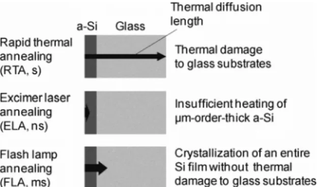
Excimer laser annealing (ELA, ns) Flash lamp annealing (FLA, ms) Insufficient heating of IJm-order-thick a-Si Crystallization of an entire Si film without thermal damage to glass substrates
Fig. 2 Schematics of rapid crystallization of a-Si by RTA, ELA, and FLA.
such as rapid thermal annealing (RTA) or excimer laser annealing (ELA), FLA is a millisecond-order treatment within which the thermal diffusion lengths of a-Si and glass are both several tens of IJm, resulting in crystallization of micrometer-order-thick a-Si without entire heating of glass substrates as illustrated in Fig. 2. We have already clarified that 4.5-lJm-thick a-Si films on quartz and soda lime glass substrates are successfully crystallized by FLA [5, 6]. We demonstrate the prototype solar cell formed using this poly-Si through the process proposed above.
EXPERIMENTAL DETAILS
We first formed a Cr film on glass substrates for improvement of adhesion as well as for back electrodes and back reflectors in a solar cell structure. Precursor n-, i-, and p-type stacked a-Si films with thicknesses of 10 nm, 4.5 IJm, 10 nm, respectively, were deposited in this sequence by Cat-CVD, the method of which realizes a-Si with hydrogen content of as low as 3%, and enables us to skip a dehydrogenation process prior to FLA. Only one shot of FLA within 10 ms duration was treated to each stacked a-Si structure. HPWVA was treated to the formed poly-Si at a pressure of 0.9 MPa at 400°C for 10
min. Diffusion of dopant and Cr atoms were
characterized by SIMS.
RESULTS AND DISCUSSION
Figures 3(a) and (b) show the surface and the Raman spectrum of the poly-Si after FLA of p-i-n stacked a-Si films, showing no peeling of Si and formation of poly-Si with high crystallinity close to unity. This crystallization is not due to the metal-induced crystallization since similar crystallization occurs even when a silicon nitride film is inserted between the Si and Cr films. We have also confirmed crystallization of a-Si even close to the SilCr interface [7]. The microwave photoconductivity decay (IJ-PCD) measurement has revealed that the intrinsic poly-Si films formed by this technique have minority carrier lifetimes of about 10 IJs after HPWVA as has been previously reported [8]. Assuming the minority carrier mobility of 14
cm
2Ns
estimated by Hall measurement of460 480 500 520 540 560 Raman shift (cm·') Fig. 3 (a) Surface and (b) Raman spectrum of the p-i-n stacked Si after FLA.
978-1-4244-1641-7/08/$25.00 ©2008 IEEE
independently prepared n-type poly-Si formed directly on glass substrates, we obtained the minority carrier diffusion length of the poly-Si of about 19 IJm, which is four times larger than its film thickness.
Figure 4 shows SIMS profiles of Cr and P atoms in the bottom layers and of B in the surface doping layer before and after FLA. The abrupt profiles of the surface B atoms as well as of the bottom Cr and P atoms are maintained after FLA, which shows possibility of immediate formation of p-i-n poly-Si structure with only one irradiation of flash lamp for p-i-n stacked a-Si layers.
We have measured the dark and 1-sun-illuminated I-V curves of the p-i-n structures before and after HPWVA. In spite of no surface passivation and the unoptimized process, clear diode feature and photocurrent are seen in the device after HPWVA. The present solar cells properties are summarized in Table 1. The detailed I-V characteristics are summarized elsewhere [9]. The relatively poor solar cell properties are probably due to the
unoptimized fabrication process and no surface
passivation. Taking into account the excellent
fundamental properties of the poly-Si such as the carrier lifetime and the mobility, further optimization of the solar
llf (a) Chromium (b) Phosphorus
Before FLA ... Before FLA
l'
1 if'-
AfterFLA 10'10"" E , - AfterFLA~ ~
I
'"
'"
E 10" E.s
.s
10" ~ ~ , I:: 10'8 I:: 0 0~
I:: 1017~
I:: 10'8!
Q) Q) u U I:: I:: 0 1018 0 (J (J 10'5 10" ~.5 0.0 0.5 1.0 1.5 0.0 Thickness (~LIll) llf (c) Boronl'
Before FLA 1 if' AfterFLA u Cil E~
10" I:: 0 10'8~
Q) U 1017 I:: 0 (J 10'6 0.0 0.1 0.2 Thickness (~m)Fig. 4 SIMS profiles of (a) Cr, (b) P, and (c) B atoms before and after FLA.
Table 1. Present performance of the poly-Si solar cells. Jse (mA) 7.15 Voc (V) 0.21 FF 0.404 Eff. (%) 0.606 cell process will lead to high-efficiency solar cells using this poly-Si.
Figure 5 shows the I-V characteristics of the poly-Si solar cells before and after light soaking under AM 1.5 1-sun irradiation for 24 hours. No significant light-induced degradation occurs in the poly-Si solar cells, showing high stability for light soaking.
i
2I:
.__ Before light soaking - After light soaking
~ Or---~---~~ ..ci
....
~ ~ -2 ·00 I: ~-41:
~
~ () -0.10 0.00 0.10 0.20 Voltage (V)Fig. 5 I-V characteristics of the poly-Si solar cell before and after light soaking.
SUMMARY
We have proposed the novel concept of fabricating thin-film solar cells on glass substrates using the IJm-order-thick poly-Si films formed by FLA of precursor a-Si films. The Cr films inserted between Si and glass, acting as adhesion layers during FLA, can be utilized as back electrodes in the solar cell structure. No significant diffusion of dopant atoms as well as Cr atoms can be seen after FLA. The fabricated p-i-n poly-Si structures work as diodes and solar cells after defect termination by HPWVA. This solar cell also shows no light-induced degradation during light soaking under AM1.5 1-sun irradiation. These facts demonstrate high feasibility of this new process for solar cell fabrication.
ACKNOWLEDGMENTS
The authors acknowledge T. Owada and T. Yokomori of Ushio Inc. for their expert operation of and fruitful discussion on FLA. This work was supported by the New Energy and Industrial Technology Development
978-1-4244-1641-7/08/$25.00 ©2008 IEEE
Organization (NEDO) of Japan. REFERENCES
[1] M. J. Keevers, T. L. Young, U. Schubert, and M. A Green, "10% Efficient CSG Minimodules", Proc. 22nd European Photovoltaic Sol. Energy Cont., 2007, pp. 1783-1790.
[2] A.G. Aberle et al., "Poly-Si On Glass Thin-Film PV Research At UNSW', Proc. 22nd European Photovoltaic Sol. Energy Conf., 2007, pp. 1884-1889.
[3] L. Carnel, I. Gordon, D. Van Gestel, G. Beaucarne, and J. Poortmans, "From 1.6 To 8 % Efficient Thin-Film Polysilicon Solar Cells", Proc. 22nd European Photovoltaic Sol. Energy Conf., 2007, pp. 1880-1883. [4] I. Gordon, L. Carnel, D. Van Gestel, G. Beaucarne, J. Poortmans, L. Pinckney, and A. Mayolet, "Thin-Film Polycrystalline-Silicon Solar Cells On Glass-Ceramics", Proc. 22nd European Photovoltaic Sol. Energy Cont., 2007, pp. 1993-1996.
[5] K. Ohdaira, Y. Endo, T. Fujiwara, S. Nishizaki, and H. Matsumura, "Formation of Highly Uniform Micrometer-Order-Thick Polycrystalline Silicon Films by Flash Lamp Annealing of Amorphous Silicon on Glass Substrates", Jpn. J. Appl. Phys. 46, 2007, pp. 7603-7606. [6] K. Ohdaira, T. Fujiwara, Y. Endo, S. Nishizaki, and H. Matsumura, "Formation of Several-Micrometer-Thick Polycrystalline Silicon Films on Soda Lime Glass by Flash Lamp Annealing", Jpn. J. Appl. Phys. 47, 2008, pp. 8239-8242.
[7] T. Fujiwara, Y Endo, S. Nishizaki, K. Ohdaira, K.
Nishioka, and H. Matsumura, "Feasibility Study On High Efficiency Poly-Si Thin-Film Solar Cells Formed By Flash Lamp Annealing Of Cat-CVD Amorphous Silicon", Tech. Digest 17th Int. Photovoltaic Sci. Eng. Conf., 2007, pp.1157-1158.
[8] Y. Endo, T. Fujiwara, S. Nishizaki, K. Ohdaira, K. Nishioka, and H. Matsumura, "High Quality Polycrystalline Silicon Films With Long Carrier Lifetime Prepared By Flash Lamp Annealing Of Cat-CVD Amorphous Silicon and Successive High-Pressure Water Vapor Annealing", Tech. Digest 17th Int. Photovoltaic Sci. Eng. Conf., 2007, pp.319-320.
[9] Y. Endo, T. Fujiwara, S. Nishizaki, K. Ohdaira, K. Nishioka, and H. Matsumura, submitted to Sol. Energy Mat. Sol. Cells