Japan Advanced Institute of Science and Technology
Title
Nondestructive Readout of Ferroelectric-Gate
Field-Effect Transistor Memory With an
Intermediate Electrode by Using an Improved
Operation Method
Author(s)
Horita, Susumu; Trinh, Bui Nguyen Quoc
Citation
IEEE Transactions on Electron Devices, 55(11):
3200-3207
Issue Date
2008-11
Type
Journal Article
Text version
publisher
URL
http://hdl.handle.net/10119/5037
Rights
Copyright (C) 2008 IEEE. Reprinted from IEEE
Transactions on Electron Devices, 55(11), 2008,
3200-3207. This material is posted here with
permission of the IEEE. Such permission of the
IEEE does not in any way imply IEEE endorsement
of any of JAIST's products or services. Internal
or personal use of this material is permitted.
However, permission to reprint/republish this
material for advertising or promotional purposes
or for creating new collective works for resale
or redistribution must be obtained from the IEEE
by writing to [email protected]. By
choosing to view this document, you agree to all
provisions of the copyright laws protecting it.
Description
Nondestructive Readout of Ferroelectric-Gate
Field-Effect Transistor Memory With an Intermediate
Electrode by Using an Improved Operation Method
Susumu Horita and Bui Nguyen Quoc Trinh
Abstract—We investigated the reading and writing of
ferro-electric-gate field-effect transistor memory with an intermediate electrode (IF-FET) to achieve perfect nondestructive readouts. In the previous operation method, although the difference in output voltage ΔVO between positive (Pr+) and negative (Pr−)
rema-nent polarization memory states was adequate for the first reading time, the nondestructive readout for the Pr− state was seriously degraded due to the generation of nonreturning domains. In order to solve this issue, a P0
r memory state was used instead of the
previous Pr−memory state. The P0
r state was induced by applying
a pulse combined with a positive voltage (VW+) and a negative voltage (VW−). VW+was to reset the previously written memory states, and VW− was to control the amount of remanent polariza-tion. In addition, in order to extinguish perfectly the nonreturning domains, a negative voltage VR− was applied for data reading, following a positive voltage VR+, where VR+was determined for clear decoding. The appropriate heights of the writing and reading voltages were determined individually from the viewpoint of good nondestructive readout and large ΔVO. As a result, it was verified
experimentally that the reading endurance reached more than 108 cycles and that the retention time of IF-FET at 150◦C was possible to exceed ten years.
Index Terms—Ferroelectric gate, ferroelectric memory,
nonde-structive readout, reading endurance, retention.
I. INTRODUCTION
F
ERROELECTRIC-GATE field-effect transistor memory (F-FET) is well known as one of the ultimate nonvolatile memories because of its remarkable features such as nonde-structive readout, high packing density, high reading speed, and low power consumption [1]–[3] compared with 1-transitor– 1-capacitor (1T–1C) or 2-transistor–2-capacitor (2T–2C) ferro-electric random access memories (FeRAMs). Furthermore, it has advantages of low writing voltage, fast writing speed, and high endurance compared with flash memory [4]–[6]. In recent years, considerable research has been carried out on F-FET [7]–[11], but it has not been commercialized so far due to the following serious problems. First, due to an insulating buffer layer which must be inserted to prevent chemical reactionManuscript received January 23, 2008; revised July 28, 2008. Current version published October 30, 2008. The review of this paper was arranged by Editor S. Deleonibus.
The authors are with the School of Materials Science, Japan Advanced Institute of Science and Technology, Nomi 923-1292, Japan (e-mail: horita@ jaist.ac.jp).
Color versions of one or more of the figures in this paper are available online at http://ieeexplore.ieee.org.
Digital Object Identifier 10.1109/TED.2008.2003329
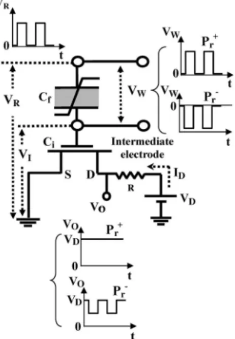
between the ferroelectric film and the Si substrate [12], [13], the ferroelectric film is subjected to a depolarization field even under a retention condition of zero bias between the ferroelec-tric gate and the Si substrate [14], [15]. This depolarization field is caused by the charges which are induced on the insulating buffer layer by the remanent polarization of the ferroelectric film. The depolarization field makes the remanent polarization of the ferroelectric film relax, leading to a short retention time [16], [17]. The second problem is high writing voltage due to the voltage drop on the buffer layer [5], [18]. To reduce the voltage drop, a high dielectric constant material (high-k material) is normally employed. Unfortunately, the interface between the high-k material and the Si substrate is poor, which leads to an unstable memory performance. In order to overcome these problems, Shimada et al. [19] has proposed a new operational principle of F-FET memory, in which an intermediate electrode for data writing is inserted between the ferroelectric gate and the buffer layer. This F-FET memory is denoted as IF-FET, and its features have been reported in detail elsewhere [20], [21]. Fig. 1 shows a schematic drawing of IF-FET, which consists of a ferroelectric capacitor (Cf) in serial
connection with a MOSFET. The input capacitance is denoted as Ci. For data writing, a voltage VWas writing pulse is applied
directly to the only Cf, using the top and intermediate
elec-trodes. The remanent polarization of Cfis set positive (Pr+) for VW> 0 or negative (Pr−) for VW< 0. For data reading, with
the intermediate electrode being electrically floated, a positive reading voltage VRas reading pulse is applied between the top
electrode and the ground or source of the MOSFET, where Cfis
connected in series with the gate of the MOSFET. By measuring the output voltages VO’s on a resistor R, the memory states can
be decoded, where the biased voltage to the drain is VDthrough R. The MOSFET acts as a reading transistor for this memory.
In general, Cffrom the Pr+state is much smaller than Cffrom
the Pr−state when Cfis applied by a positive voltage. Here, we
define the ferroelectric capacitances from the P+
r and Pr−states
as Cf land Cf h, respectively. Using a small Cf l, the intermediate
voltage VIto the ground can be lower than the threshold voltage Vthof the MOSFET or the reading transistor, so that the
transis-tor is setOFFstate or that the output voltage characteristics are flat, as shown in Fig. 1. Also, using a large Cf h, VIcan be higher
than Vth, so that the transistor is setONstate and that the drain
current IDflows. As a result, the output voltage characteristics
are pulse trains. From this operational principle, using IF-FET with the intermediate electrode, the operation voltage can be
Fig. 1. Operation principle of IF-FET memory.
lowered not only because the writing voltage is applied only to the ferroelectric capacitor but also because a high reading voltage to saturate the polarization of ferroelectric capacitor like FeRAM is not needed. Owing to this, silicon oxide can be used as a buffer layer or gate instead of high-k material, which leads to an excellent interface property with Si to obtain stable device operation. Additionally, the remanent polarization of the memory states can be protected under zero-bias condition, so that the retention time extends much longer.
So far, we used P+
r and Pr− remanent polarizations as
memory states, and a positive unipolar square pulse was applied for data reading. Although the difference in output voltage ΔVO
between P+
r and Pr−memory states was adequate for the first
reading, ΔVO decreased with the reading cycle. It has been
demonstrated that the reading endurance of IF-FET memory reaches to 106 cycles [22], which is much smaller than that of 1012cycles for FeRAM. In particular, for the Pr−state, VO
degraded very fast with the reading cycle. This is because all of the downward domains switched by reading out from the up-ward domains of the initial Pr−state do not return to the initial
upward states, and some domains still remain downward in the read-out Pr−state. These domains, which are called nonreturn-ing domains as reported before [21], make the nondestructive readout of the Pr−state degraded. For this issue, Shimada et al. used a low reading voltage without polarization reversal of the
Pr− state. However, since the low reading voltage leads to a lower output voltage than that of conventional destructive read-out FeRAMs, the operation easily fails due to degradation in ferroelectric properties such as the imprint phenomenon. In our case, however, a high-enough voltage for readout is used, which leads to destructive readout without failure.
In order to solve this issue, first, we used a memory state
Pr0 instead of a Pr− state to reduce the amount of
nonreturn-ing domains. The Pr0 memory state was proposed also by
Shimada et al. [23], [24]. The ideal state of the Pr0 state is
nonpolarized in Cf. They used the state to minimize the imprint
effect in 2T–2C FeRAMs and, essentially, for nondestructive
readout. Second, for data reading, we proposed a new combined reading pulse of a negative voltage VR− following a positive voltage VR+. While VR+produces a sufficient output voltage for decoding, VR−plays a role to return the nonreturning domains to the initial state, i.e., to recover the memory state. The effectiveness of our new operating method on nondestructive readout has already been reported roughly [25]. The report, however, does not mention the details of the operation principle and the determination process of operation parameters, e.g.,
VR+and VR−. Furthermore, other memory characteristics such as reading endurance and retention time have never been reported so far.
In this paper, at first, we explain the origin of the issue on nondestructive readout and present our original method to solve it, i.e., using the P0
r memory state and the combined
reading pulse, in detail. Next, we present and discuss the experimental results to investigate the operation parameters of the method for nondestructive readout. Finally, using the appropriate conditions, we show, for the first time, the results of reading endurance and retention characteristics under almost perfectly nondestructive readouts compared with those of the previous memory state and reading pulse.
II. IMPROVEMENT A. Origin of the Issue
In the previous operation method, VW’s with two square
pulses, e.g., of +4 or−4 V, were applied to produce the mem-ory state of P+
r or Pr−, respectively. For data reading, VR’s with
two positive unipolar square pulses, e.g., of 3.5 V, were applied. Fig. 2(a) and (b) shows the dependences of the output voltage of the P+
r state, VO(Pr+), and that of the Pr−state, VO(Pr−), for
the first, second, and tenth reading times. The read-out memory state after each reading out, from the first to the tenth time, was retained for 1 min under the condition that the intermediate electrode was electrically floated and that the top electrode and both the source and drain of the reading transistor were grounded. From Fig. 2, it can be seen that VO(Pr+) measured as VOn(Pr+) after the nth readout does not vary and has a constant
value of VD= 2 V. This memory state is nondestructive.
How-ever, VOn(Pr−) of VO(Pr−) at the nth reading time increases with n and approaches VD, which means that this memory state is
gradually changed close to P+
r and that the two memory states
become hardly distinguishable. This is due to the generation of nonreturning domains as mentioned before.
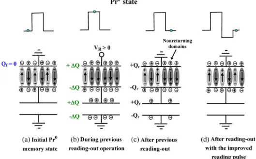
Fig. 3 shows the schematic drawings of the ferroelectric domains in Cf and stored charges on the equivalent circuits
of Cf connected in series with an input capacitor Ci of the
reading transistor for the previous reading-out process of the
Pr−memory state. Fig. 3(a)–(d) is for the initial memory state, during the reading-out operation, just after the reading out, and in a nearly steady state after the reading out, respectively. At the top of the figure, the reading pulses are schematically drawn for the (a)–(d) conditions, indicating each operation point as an individual dot. The remanent charge −Qf< 0 is stored as
an initial memory state of Pr−, as shown in Fig. 3(a). A charge
ΔQ > 0 is induced by applying a positive VR to the serial
Fig. 2. Readout characteristics of the first, second, and tenth readings, which were measured with the previous operation method. (a) For the Pr+state. (b) For
the Pr−state.
Fig. 3. Schematic drawings of ferroelectric domains in Cf and stored charges on serially connected capacitances of Cf and Cifor the previous reading-out
process of the Pr−state. (a) Initial Pr−state, (b) during the reading out, (c) just after the reading out, and (d) nearly steady state after the reading out. At the top
of the figure, the reading pulse is drawn for each state, and each operation point is indicated as a dot.
the upward domains in Fig. 3(a) are switched to the downward domains. When VR falls to zero, ΔQ stored on Ci acts as a
momentary battery to Cf, and some amount of ΔQ moves
to Cf, as shown in Fig. 3(c). Because the voltage magnitude
of the momentary battery is not as large as that of VW for
the Pr− state, some of the switched domains do not return to the initial upward state, which are nonreturning domains. That is, the ΔQ is reduced but never becomes zero. Thus, on the input capacitance Ci of the reading transistor, some
positive charge Qr remains after each reading out, as shown
in Fig. 3(d), where Qr is called a remaining charge hereafter.
Since Cf and Ci have finite huge resistances of Rf and Ri,
respectively, leakage current through Cf and Ciflows from the
charge source of Qrso that Qron Ci reduces to zero roughly
within the time constant, depending on the capacitances and resistances. However, because Qr on Cf is terminated with
ferroelectric polarized domain and is held, it never vanishes, and the initial remanent charge Qf of the Pr− state is changed
to−Qf+ Qr. Therefore, VOn(Pr−) increases with the reading
time, as shown in Fig. 2(b). On the other hand, for the P+ r state,
there is a small amount of remaining charge on Ciafter reading
out because most of the domains in this memory state are downward and the domains switched by VRare few. Moreover,
since the reading operation in this state acts as the rewriting operation, the nondestructive readout is performed without failure. Therefore, we can conclude that it is necessary to suppress the generation of nonreturning domains after reading out for the sake of the nondestructive readout of the Pr−state.
B. Improvement of Memory State and Reading Pulse
In order to solve the issue on nondestructive readout of IF-FET [25], instead of a Pr− state, we use a P0
r state whose
position in the P−E hysteresis loop is not exact but near the origin, as shown in Fig. 4(a). The P0
r state can be produced by
a combined pulse consisting of a positive part (VW+) followed by a negative part (VW−), as shown in Fig. 4(b). VW+ acts as a reset pulse to the data-written memory cell. Increasing |VW−| increases the number of upward domains switched from the downward domains produced by VW+, and the magnitude of VW− can control a total polarization charge on Cf. In order to
sup-press the generation of nonreturning domains,|VW−| should be reduced to limit the number of upward domains. However, re-ducing|VW−| excessively makes the memory state approach the
P+
r state, and the difference in VObetween both memory states
Fig. 4. (a) Schematic major P−E hysteresis loop with a minor loop showing a reading operation trace of the P0
r state, (b) writing pulse to produce the Pr0state,
and (c) improved reading pulse. Points A and B in (a) correspond to points A and B, respectively, of the improved reading pulse in (c).
Fig. 5. Schematic drawings of ferroelectric domains in Cf and stored charges on Cf and Cifor the reading-out process of the Pr0state. (a) Initial Pr0state,
(b) and (c) during and after the reading out with the previous reading pulse, respectively, and (d) after the reading out with the improved reading pulse consisting of a positive voltage and a negative voltage. At the top of the figure, the reading pulse is drawn for each state, and each operation point is indicated as a dot.
Therefore, there is an appropriate|VW−|, for which the P0 r state
is probably near the origin of P−E hysteresis loop, as shown in Fig. 4(a). Even if the P0
r state is used, nonreturning domains
are still generated as long as the previous reading pulse is used, where the amount after reading out is much smaller compared with that of the Pr−state. These charge states are schematically shown in Fig. 5 (as in Fig. 3). In this case, the P0
r state is
nonpolarized so that the volume of upward domains is equal to that of downward domains. In order to return Qron Cito Cf
as the initial memory state, we use a combined reading pulse consisting of a negative VR−following a positive VR+, as shown in Fig. 4(c). VR+ is used for data decoding, and VR− acts as a rewriting operation for the Pr0 state. The operation points of
polarization–voltage (P−V ) hysteresis loop corresponding to
VR+(A) and VR−(B) in Fig. 4(c) are indicated as dots of A and B, in Fig. 4(a), respectively, and the reading operation traces a minor loop. By using this combined pulse, Qron Ci, as well as
on Cf, is reduced to zero, and the read-out Pr0state can return
to the initial memory state, as shown in Fig. 5(d), which means that nondestructive readout can be complemented. Here, we notice that|VR−| should be small enough in order not to destroy the P+
r memory state. This is because an excessively large|VR−|
can switch some amount of downward domains of the P+ r state
to upward domains, and a nonnegligible remaining charge is stored on Ci due to nonreturning domains like in the Pr− case.
Therefore, there is an appropriate|VR−| in the combined reading pulse, where|VR−| depends on |VW−| which determines the actual
Pr0memory state.
III. EXPERIMENTALSETUP
The discrete circuit based on Fig. 1 was used to determine the appropriate VW+, VW−, VR+, and VR− for the nondestructive readout of IF-FET memory. The output voltage VO was
mea-sured on a resistor of 2 kΩ connected with the drain of the MOSFET, which was biased by a dc voltage VD of 2 V. In
this circuit, we used an n-channel commercial MOSFET with
Vth= 1.4 V and Ci= 180 pF. The preparation of Cfconsisting
of (RuOxtop electrode)/ PZT/ (Pt/RuOxbottom electrode) on
the SiO2/Si substrate was described in our previous report [26].
The ferroelectric layer was a 200-nm-thick and highly (100)/(001)-oriented PZT film. The leakage current density of Cf is approximately 10−5 A/cm2 at the applied voltage
to estimate not only the IF-FET performance but also the appropriate writing and reading voltages, P−V measurements of Cfwere performed using a Sawyer–Tower circuit with a sine
wave at 100 Hz. The applied voltage VW+ was determined so that it would be not only enough to saturate the polarization of Cf but also as low as possible for low-voltage operation. VR+ was determined for decoding the memory states more distinctly, in which the intermediate VI nearly became Vth of
the MOSFET, or VO(Pr+) hardly responded to the reading
pulse and almost kept VD. As for VW−, at first, from the two
viewpoints of suppressing nonreturning domain generation and increasing ΔVO = VO(Pr+)− VO(Pr−), the difference in VO
between the P+
r and Pr− states, we investigated to obtain the
appropriate range by using the previous positive reading pulse. Then, both VW−and VR−were determined simultaneously so that a nondestructive readout could be achieved, with ΔVO being
as large as possible. After determining the four appropriate voltages of the writing and reading pulses, the reading en-durance was analyzed. The memory states of P+
r and Pr0were
read out continuously up to 108 times by using the combined reading pulse with the frequency of 10 kHz. Also, the retention characteristics were investigated. The two samples of Pr+ and
Pr0states were stored at 150◦C in air for a maximum duration of 24 h, and the retention time was estimated by means of an extrapolation method.
IV. RESULTS ANDDISCUSSION A. Determination of the Pulse Heights of Writing and Reading Pulses
1) VW+ and VR+: From the measured hysteresis loop, we
obtain the dependences of the twice remanent polarization 2Pr and of the coercive voltage Vc on the voltage applied
to the ferroelectric capacitor. By this measurement, VW+ was determined to be 4 V, around which 2Pr and Vc began to
saturate. For distinct memory operation, the gate voltage of the MOSFET for the Pr+ memory state, VI(Pr+) at applying V
+ R
of the combined reading pulse, should be equal to or a little smaller than the threshold voltage of the MOSFET. Since Cf l
is much smaller than Cf hfrom Pr0in general, this criterion for VR+ is automatically satisfied for the Pr0 state, which brings a
clear inverse response to the reading pulse.
Using the measured P−V hysteresis loop and the device parameters of the MOSFET, we calculated VR+ = 3.5 V, where
Cf h and Cf l were roughly estimated to be 155 and 104 pF,
respectively. Also, we confirmed experimentally that this value of VR+was adequate for memory operation.
2) VW− and VR−: Fig. 6 shows |VW−| dependences of ΔV1 O
and ΔVO1−2(P0
r). ΔVO1is the difference in VObetween the Pr+
and P0
r states at the first reading time, and ΔVO1−2(Pr0) is the
difference in VOof the Pr0state between the first and the second
reading time. The 1–2 superscript indicates the reading times of the first to the second. In this case, VW+= 4 V, VR+= 3.5 V, and
VR−= 0 which is the previous reading pulse. From this figure, we can see that ΔVO1increases with|VW−| because Cf hwhich
is proportional to the volume of the upward domain increases with |VW−|. It is noted that the increment of ΔV1
O increases
steeply around |VW−| between 2 and 2.5 V. This means that,
Fig. 6. |VW−| dependences of ΔV1 O= VO1(P + r )− VO1(Pr0) and ΔVO1−2(P0 r) = VO2(Pr0)− VO1(Pr0). ΔVO1 is the difference in VO
between the Pr+and Pr0states at the first reading, and ΔVO1−2(P 0 r) is the
difference in VOof the Pr0state between the first and the second reading time.
In this case, the previous reading pulse with VR−= 0 was used.
in this range, the polarity of the remanent polarization of the
P0
r state is probably changed from positive to negative and
that the fraction of the domain switching from downward to upward per unit of |VW−| is the largest. We can also see from this figure that ΔVO1−2(Pr0) increases gradually with|VW−| up to 2.5 V and then abruptly increases from|VW−| = 2.5 to 3 V. This abrupt increase indicates that the nonreturning domains are significantly generated in the range of 2.5–3 V. Therefore, from the result of Fig. 6, it can be said that the appropriate|VW−| is located near 2.5 V. The next step to seek for more appropriate
VW− was performed simultaneously with VR−.
Fig. 7(a) shows the typical dependences of the output volt-ages VO(Pr+) and VO(Pr0) for the Pr+ and Pr0 states,
respec-tively, on the number of reading times for different values of
VR−, where VR−= 0,−1, −1.8, −2.1, and −3 V. For the P0 r
state, VW+= 4 V and VW− =−2.6 V were used. It can be seen from this figure that VO(Pr+) at VR−≥ −2.1 V is constant and
does not vary with the number of reading times. However, at VR−=−3 V, it decreases gradually with the reading time, which means that increasing|VR−| over 2.1 V induces a nonre-turning domain even in the Pr+state and degrades the memory
state. On the other hand, although VO(Pr0) increases with the
reading time at VR−≥ −1.8 V, the increment decreases with
|V−
R|. This is because the volume of the nonreturning domain
is reduced with increasing|VR−|. Moreover, at VR−=−2.1 and
−3 V, VO(Pr0) is kept constant and does not change for any
number of reading times, which means that the generation of the nonreturning domain is completely suppressed for the P0 r
state. From this result, at|VR−| = 2.1 V, the difference between
Vn
O(Pr+) and VOn(Pr0), ΔVOn, remains constant, and both
mem-ory states are stable to the ten reading times. Otherwise, ΔVn O
decreases due to reading out, which is unfavorable for data decoding as memory device. The saturation of Vn
O(Pr+) and VOn(Pr0) with the reading time means that the new memory states are rebuilt from the initial memory states by applying reading pulse consecutively. These new states result from bal-ance in volume of the domain switched between upward and downward due to the application of the combined reading pulse.
Fig. 7(b) shows the dependences of ΔV10
O = VO10(Pr+)− V10
Fig. 7. (a) Characteristics of output voltage VO for the Pr+ and Pr0 states
versus the number of readings for different values of VR−with VW−=−2.6 V, and (b)|VR−| dependences of ΔVO10= V10 O (P + r )− VO10(P 0 r) for VW−= −2.5 and −2.6 V. ΔV10
O is the difference in VO between the Pr+ and Pr0
states at the tenth reading. In this case, VW+= 4 V and VR+= 3.5 V.
at the tenth reading, on VR−for VW−=−2.5 and −2.6 V. From these characteristics, we can find better values of VW− and VR− from a viewpoint of distinct memory operation. Around|VR−| = 2.1 V, ΔVO10for both VW−values reach the maximum values be-cause of almost-perfect suppression of the nonreturning domain for their memory states, as mentioned earlier. Also, because ΔV10
O for VW− =−2.6 V is larger than that for VW− =−2.5 V,
the former value of VW− is more desirable.
By investigating the pulse heights as mentioned previously, as appropriate operation parameters, we determined VW+= 4 V and VW− =−2.6 V for the P0
r state, and VR+= 3.5 V and VR−=−2.1 V for the combined reading pulse. The voltage ranges for the writing and reading pulses seem narrow if the memory array requires the largest ΔVO under nondestructive
readout. However, if ΔVO is not required to be the largest but
large enough for the sense signal, their ranges are probably not so narrow in practice. The operation voltages, e.g., VW− and VR−, strongly depend on not only memory structure such as ferroelectric thickness, Ci, transconductance of the reading
transistor, and so on, but also ferroelectric properties such as
Cf h, Cf l, Ec, curvature of P−V loop, and so on. Therefore,
the range of operation voltage can be extended so that the memory array of IF-FET is commercialized, provided that the memory structure and ferroelectric properties of Cf are
improved properly.
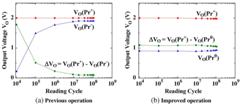
B. Read-Out Characteristics
Fig. 8 shows the comparison of reading endurance charac-teristics between (a) the previous operation method and (b) the
improved method in this paper, where, in the previous method,
VW= 4 V for the Pr+state, VW=−4 V for the Pr−state, and VR= 3.5 V. We can see from Fig. 8(a) that, although VO(Pr+)
is constant, VO(Pr−) quickly increases with the reading cycle
because the Pr− state is degraded due to the generation of nonreturning domains. As a result, above 104 reading cycles, ΔVO= VO(Pr+)− VO(Pr0) is reduced to small value of less
than 0.11 V, which is too small to distinguish both memory states. Therefore, we can say that the reading endurance of the previous operation is very poor. However, by using our improved operation method, the reading endurance is extended significantly to over 108reading cycles, as shown in Fig. 8(b), because the P0
r state can be recovered after each reading cycle.
Although the output voltage VO(Pr+) remains even above 108
reading cycles, VO(Pr0) increases slightly. One possible reason
for this is quality degradation of the PZT film due to a number of reading cycles. For example, if the P−E hysteresis loop is shifted toward the negative voltage side, the P0
r memory
state approaches the P+
r state, and VO(Pr0) increases. In order
to prevent this phenomenon, the quality of the ferroelectric film should be more stabilized. From this result, it can be concluded that our improved operation method is very effective for the reading endurance. Using a high-quality ferroelectric film like a commercial film, the intrinsic reading endurance is expected to be 1012−1013cycles, which is the reported value for FeRAM in general. We reported in our previous papers that the reading endurance is about 106 cycles for the Pr− state, but the result of Fig. 8(a) shows a much smaller number of cycles of the endurance than this [21], [22]. The MOSFET used previously was not commercial, but was home-made, and it was connected with the diodes to simulate a writing transistor. Although the commercial MOSFET used in this paper is not connected with either a writing transistor or diodes, it has a protection circuit composed of diodes connected between the source and the gate and between the drain and the gate. The leakage current of the protection circuit is much larger than that of the simulation diodes by about two orders of magnitude. The leakage current which supplies some negative charge on the intermediate electrode degrades the Pr− state at each reading
operation. Therefore, the Pr−state in this study was destroyed
more quickly than the previous one. Taking this into account, we can also say that the improved operation method overcomes drawbacks due to an inevitable small leakage current through the MOSFET gate.
Even in the previous memory states of P+
r and Pr−, it seems
that nearly nondestructive readout is possible without using a
P0
r state if VR+ and VR− pulses with the optimized heights are
used. In order to return the read-out Pr−state to the initial state almost without the nonreturning domain, we need such a high
|V−
R| that the Pr+state may change negative and be destroyed.
It was found that VR− brought the P+
r state close to the Pr−
one to suppress the nonreturning domain in the Pr−state, which is a destructive readout. Therefore, it can be concluded that a nondestructive readout is impossible without using a Pr0state.
Also, using a Pr0 state is more favorable with respect to
low-power consumption, because|VR−| for Pr0is lower.
Fig. 9 shows the retention characteristics of the P+ r and P0
Fig. 8. Reading endurance characteristics of (a) the previous operation method and (b) the improved operation method. In (a), VW= 4 V for the Pr+state,
VW=−4 V for the Pr−state, and VR= 3.5 V for the reading out. In (b), VW= 4 V for the Pr+state, VW+= 4 V and VW−=−2.6 V for the Pr0state, and
VR+= 3.5 V and VR−=−2.1 V for the reading out.
Fig. 9. Retention characteristics for the improved operation method. VW=
4 V for the Pr+state, VW+= 4 V and VW−=−2.6 V for the P 0
r state, and
VR+= 3.5 V and VR−=−2.1 V for the reading out.
writing, the two memory states were stored at 150◦C in air for various retention times up to 24 h. We can see from this figure that VO(Pr+) decreases more quickly than VO(Pr0) increases
with the retention time. Since the P+
r state has a much higher
energy of electric static potential than the ground state, it is gradually depolarized by thermal energy. In contrast with the
Pr+ state, the Pr0 state is much stabler in energy because it is
little polarized, which can lead to a stable output signal for a long retention time. As a possible reason for the slight increase in VO(Pr0) with the retention time, it can be considered that
the initial P0
r state is not perfectly nonpolarized and that the
ferroelectric property is slightly changed due to the storage at 150 ◦C. Extrapolating the fitting lines along the data for the
P+
r and Pr0 states individually, as shown in Fig. 9, we can
estimate that ΔVO= VO(Pr+)− VO(Pr0) will be larger than
0.4 V even after a ten-year storage at 150◦C. As ΔVO= 0.4 V
is a sufficient signal to distinguish the memory state, it can be said that IF-FET memory has good retention characteristics. This results not only from the nondepolarization field in the fer-roelectric film during retention like FeRAM but also from using the energetically stabler Pr0state with almost nonpolarization.
Therefore, IF-FET memory can solve the serious problem of short retention time which prevails in the conventional F-FET memory.
In an actual memory array, writing and reading disturbances should be avoided. In the case of IF-FET, since combined
reading pulse serves nondestructive readout, reading distur-bance can be negligible. However, the writing disturdistur-bance, in particular, of the P0
r state due to Pr+ writing is serious.
Because P+
r -writing pulse is always positive, the nonpolarized
state of Pr0may change to positive and approach the Pr+state with repeating Pr+ writing. If the nonselected memory cell is electrically floated perfectly or the plate line of the nonselected cell is biased positively corresponding to the Pr+-writing pulse,
the writing disturbance of the Pr0 state might be free.
How-ever, these compensation operations for disturbance free are complicated and difficult technically. In order to suppress P0 r
disturbance due to P+
r writing practically, we should investigate
in the future.
V. CONCLUSION
We investigated the reading and writing of IF-FET in order to achieve perfect nondestructive readouts. In the previous op-eration method, although the difference in output voltage ΔVO
between the P+
r and Pr−states is sufficient at the first reading
time, the nondestructive readout for the Pr− state is seriously degraded because of large amounts of remaining charge Qron Cidue to the nonreturning domains generated after reading out.
In order to reduce Qr, the Pr0state was used as a new memory
state instead of the Pr− state. The Pr0 state was induced by
applying a pulse combined with a positive voltage VW+ and a negative voltage VW−. VW+ was to reset the previously written memory states, and VW− was to control the amount of rema-nent polarization. When the negative remarema-nent polarization is smaller, Qris also smaller. However, ΔVOmeasured by reading
out is too small to decode the memory state. In order to both maintain a large ΔVO and suppress Qr sufficiently, for data
reading, a negative voltage VR−was applied following a positive voltage VR+ which was determined for distinct decoding. By increasing|VR−|, the downward domains switched by VR+can be returned to the initial upward domains, and the Pr0state can be recovered after each reading. However, excessive|VR−| destroys the Pr+state. Therefore, we investigated in detail the heights of VW− and VR− from the viewpoint of zero Qr and large ΔVO.
Under appropriate conditions, where VW+= 4 V, VW− =
−2.6 V, V+
R = 3.5 V, and VR−=−2.1 V, nondestructive
it was verified experimentally that the reading endurance can reach more than 108 cycles. This result indicates that the intrinsic endurance of IF-FET is expected to be more than 1012 cycles, which is comparable with that of FeRAM. Furthermore, it was shown that the retention time of IF-FET at 150◦C can exceed about ten years. From these results, we can conclude that IF-FET memory array can be a very promising candidate for future memories if the writing disturbance is sufficiently prevented.
ACKNOWLEDGMENT
The authors would like to thank K. Nishioka of the University of Miyazaki, Miyazaki, Japan, for the helpful discussions and his technical support.
REFERENCES
[1] J. F. Scott and C. A. Paz de Arauzo, “Ferroelectric memories,” Science, vol. 246, no. 4936, pp. 1400–1405, Dec. 1989.
[2] S. Mathews, R. Ramesh, T. Venkatesan, and J. Benedetto, “Ferroelec-tric field effect transistor based on epitaxial perovskite heterostructures,” Science, vol. 276, no. 5310, pp. 238–240, Apr. 1997.
[3] H. Ishiwara, “Current status and prospects of FET-type ferroelectric mem-ories,” J. Semicond. Technol. Sci., vol. 1, no. 1, pp. 1–14, Mar. 2001. [4] Y. Fujimori, T. Nakamura, and A. Kamisawa, “Properties of
ferroelec-tric memory FET using Sr2(Ta, Nb)2O7thin film,” Jpn. J. Appl. Phys.,
vol. 38, no. 4B, pp. 2285–2288, 1999.
[5] T. Hirai, Y. Fujisaki, K. Nagashima, H. Koike, and Y. Tarui, “Prepa-ration of SrBi2Ta2O9 film at low temperatures and fabrication of a
metal/ferroelectric/insulator/semiconductor field effect transistor using Al/SrBi2Ta2O9/CeO2/Si(100) structures,” Jpn. J. Appl. Phys., vol. 36,
pp. 5908–5911, Jul. 1997.
[6] International Technology Road Map for Semiconductors (ITRS), pp. 8–10, 2005. [Online]. Available: http://www.itrs.net/Links/2005ITRS/ ERD2005.pdf
[7] S.-M. Yoon and H. Ishiwara, “Memory operations of 1T2C-type ferro-electric memory cell with excellent data retention characteristics,” IEEE Trans. Electron Devices, vol. 48, no. 9, pp. 2002–2008, Sep. 2001. [8] S. B. Xiong and S. Sakai, “Memory properties of SrBi2Ta2O9 thin
film prepared on SiO2/Si substrates,” Appl. Phys. Lett., vol. 75, no. 11,
pp. 1613–1615, Sep. 1999.
[9] T. Nakamura, Y. Nakao, A. Kamisawa, and H. Takasu, “Ferroelectric memory FET with Ir/IrO2electrodes,” Integr. Ferroelectr., vol. 9, no. 1–3,
pp. 179–187, Jun. 1995.
[10] H. Saiki and E. Tokumitsu, “Ferroelectric split-gate-field-effect-transistors for nonvolatile memory cell array: New era of nonvolatile memories,” IEICE Trans. Electron., vol. 87, no. 10, pp. 1700–1705, Oct. 2004.
[11] K.-H. Kim, J.-P. Han, S.-W. Jung, and T. P. Ma, “Ferroelectric DRAM (FEDRAM) FET with metal/SrBi2Ta2O9/SiN/Si gate structure,” IEEE
Electron Device Lett., vol. 23, no. 2, pp. 82–84, Feb. 2002.
[12] Y. Matsui, M. Okuyama, M. Noda, and Y. Hamakawa, “A study of elec-tronic states near the interface in ferroelectric-semiconductor heterojunc-tion prepared by RF sputtering of PbTiO3,” Appl. Phys., A Mater. Sci.
Process., vol. 28, no. 3, pp. 161–166, Jul. 1982.
[13] T. Inoue, Y. Yamamoto, S. Koyama, and S. Suzuki, “Epitaxial growth of CeO2layers on silicon,” Appl. Phys. Lett., vol. 56, no. 14, pp. 1332–1333,
Apr. 1990.
[14] J. M. Benedetto, R. A. Moore, and F. B. McLean, “Effects of operating conditions on the fast-decay component of the retained polarization in lead zirconate titanate thin films,” J. Appl. Phys., vol. 75, no. 1, pp. 460– 466, Jan. 1994.
[15] K.-W. Lee and W.-J. Lee, “Relaxation of remanent polarization in Pb(Zr,Ti)O3thin film capacitors,” Jpn. J. Appl. Phys., vol. 41, no. 11B,
pp. 6718–6723, Nov. 2002.
[16] T. P. Ma, J.-P. Han, “Why is nonvolatile ferroelectric memory field-effect transistor still elusive?” IEEE Electron Device Lett., vol. 23, no. 7, pp. 386–388, Jul. 2002.
[17] C. T. Black, C. Farrell, and T. J. Licata, “Suppression of ferroelectric po-larization by an adjustable depopo-larization field,” Appl. Phys. Lett., vol. 71, no. 14, pp. 2041–2043, Oct. 1997.
[18] B. Park, S. Shouriki, E. Tokumitsu, and H. Ishiwara, “Fabrication of PbZrxTi1−xO3 films on Si structures using Y2O3buffer layers,” Jpn.
J. Appl. Phys., vol. 37, pp. 5145–5149, 1998.
[19] Y. Shimada, Y. Kato, T. Yamada, K. Tanaka, T. Ostuki, Z. Chen, M. Lim, V. Joshi, L. McMillian, and C. Paz de Araujo, “High density and long re-tention non-destructive readout FeRAM using a linked cell architecture,” Integr. Ferroelectr., vol. 40, no. 1–5, pp. 41–54, 2001.
[20] S. Horita and T. D. Khoa, “Gate voltage reduction of a ferroelectric gate field-effect transistor memory with an intermediate electrode on data-reading,” Jpn. J. Appl. Phys., vol. 42, no. 4A, pp. L365–L368, 2003. [21] T. D. Khoa and S. Horita, “Analysis on operation of a F-FET memory with
an intermediate electrode,” IEEE Trans. Electron Devices, vol. 51, no. 5, pp. 820–823, May 2004.
[22] T. D. Khoa and S. Horita, “Retention and read endurance characteristics of a ferroelectric gate field effect transistor memory with an intermediate electrode,” Jpn. J. Appl. Phys., vol. 43, no. 4B, pp. 2220–2225, 2004. [23] T. Yamada, Y. Kato, S. Koyama, and Y. Shimada, “Long-term stabilization
of sense signals in a nondestructive readout FeRAM by intentional modi-fication of the polarization hysteresis curve for low voltage applications,” in Proc. Ext. Abstr. Int. Conf. Solid State Devices Mater., Tokyo, Japan, 2003, pp. 34–35.
[24] S. Koyama, Y. Kato, T. Yamada, and Y. Shimada, “Improvement in readout reliability of a nondestructive readout FeRAM by asymmetrical programming,” in Proc. Int. Meeting Future Electron Devices, Kansai, Japan, 2004, pp. 125–126.
[25] B. N. Q. Trinh and S. Horita, “Improvement of nondestructive readout of ferroelectric gate FET memory with an intermediate electrode by using new data writing and reading methods,” in Proc. 16th IEEE ISAF, Nara, Japan, 2007, pp. 58–61.
[26] B. N. Q. Trinh and S. Horita, “Operation of ferroelectric gate field-effect transistor memory with intermediate electrode using polycrystalline capacitor and metal–oxide–semiconductor field-effect transistor,” Jpn. J. Appl. Phys., vol. 45, no. 9B, pp. 7341–7344, 2006.
Susumu Horita was born in Toyama, Japan, in 1959.
He received the B.S. degree in electrical engineer-ing from Kanazawa University, Kanazawa, Japan, in 1982 and the M.S. and Ph.D. degrees in applied elec-tronics from Tokyo Institute of Technology, Tokyo, Japan, in 1984 and 1987, respectively.
In 1987, he was with the Department of Electrical and Computer Engineering, Kanazawa University, as a Research Associate and was a Lecturer and an Associate Professor in 1988 and 1992, respectively. Since 1995, he has been an Associate Professor with the School of Materials Science, Japan Advanced Institute of Science and Technology, Nomi, Japan. His research interests include ferroelectric memory, thin-film transistors, and film formation process of electron device.
Dr. Horita is a member of the Materials Research Society, the Japan Society of Applied Physics, the Surface Science Society of Japan, and the Institute of Electronics Information and Communication Engineers.
Bui Nguyen Quoc Trinh was born in Bacgiang City,
Vietnam, in 1980. He received the B.S. and M.S. degrees in solid-state physics from the Faculty of Physics, Hanoi University of Science, Vietnam Na-tional University, Hanoi, Vietnam, in 2002 and 2004, respectively, and the Ph.D. degree from the School of Materials Science, Japan Advanced Institute of Science and Technology, Nomi, Japan, in 2007. His Ph.D. dissertation focused on the fabrication of inte-grated ferroelectric gate field-effect transistor mem-ory with an intermediate electrode.
Currently, he is with the Laboratory of Semiconductor Materials as a Re-search Fellow at the School of Materials Science, Japan Advanced Institute of Science and Technology. His research interests include characterizations of ferroelectric thin films, ferroelectric devices, and process technologies for Si-related devices.