Interconnection Networks for High-Performance
Stream Computing with FPGA Clusters
著者
Mondigo Antoniette Pangilinan
学位授与機関
Tohoku University
学位授与番号
11301甲第19337号
TOHOKU UNIVERSITY
Graduate School of Information Sciences
Interconnection Networks for High-Performance
Stream Computing with FPGA Clusters
(FPGA
クラスタによる高性能ストリーム計算の
ための相互接続網に関する研究)
A dissertation submitted for the degree of Doctor of Philosophy
(Information Sciences)
Department of Computer and Mathematical Sciences
by
Antoniette Pangilinan MONDIGO
Abstract
Interconnection Networks for High-Performance
Stream Computing with FPGA Clusters
Antoniette Pangilinan MONDIGO
Abstract
High Performance Computing (HPC), as a field that relies heavily on cutting-edge technologies, is among the various domains affected by the impending end of Moore’s Law and Dennard scaling. Many advancements in computing architecture across the various technology stack levels are being considered and explored to meet and support the growing demands of HPC applications. Field Programmable Gate Arrays (FPGAs), along with other dedicated acceleration platforms, are playing significant roles in this endeavor.
FPGAs, as reconfigurable devices, are recently seen as promising, energy-efficient hard-ware solutions due to a good balance between their flexibility and efficiency characteristics. Despite their typical lower operating frequency range than the other traditional platforms’, creating custom hardware allows massively parallel operations with high utilization rates. Fine-grained and coarse-grained parallelism could be enabled and exploited by creating deep and wide computing pipelines with regular memory accesses. This allows continuous data streams to pass through the pipelines, while increasing the number of operations per memory access; therefore, fully utilizing the available bandwidth. All these make stream computing with a data flow model suitable for low operational intensity applications, such as stencil computing algorithms in FPGAs, which has been successfully demonstrated in numerous case studies. However, the resource budget of a single FPGA limits further performance scaling.
Just as clustered architectures dominate the current HPC trends, the utilization of
FPGA clusters is a promising approach. However, despite numerous, successful case
studies, FPGAs still lack widespread acceptance in general-purpose HPC installations. With this premise, it is the general direction of this research to aim at making FPGAs accelerators of HPC offloaded applications through system-wide custom computing. In order to achieve high performance, the main strategies are to increase the design space to support the increase of processing units, to reduce interconnection overhead, and to improve HPC application algorithms through customization. In this regard, stream com-puting with data flow is a suitable approach to fully exploit FPGA capabilities to meet
Abstract
high performance and high scalability demands in HPC.
Recently, large-scale deployments of FPGA clusters in data centers and cloud ser-vices have demonstrated the feasibility of providing a system-wide custom computing infrastructure with FPGAs. However, the inter-FPGA interconnection network is an overhead-inducing region in the extended design space, which could affect the overall per-formance. Thus, there is a need to investigate a network’s performance characteristics in order to achieve low-latency and throughput communication, especially for high-performance stream computing. Since the clustering architecture of FPGAs is typically selected based on target workloads and its required performance, choosing an appropriate interconnection network for FPGA clusters becomes an important aspect in this research. This dissertation is focused on investigating scalable interconnection networks for high-performance stream computing FPGA clusters. In particular, this dissertation focuses on the comparison of direct and indirect networks, with specific focus for stream computing requirements.
The main objective of this dissertation is to explore appropriate interconnection net-works for high-performance stream computing FPGA clusters, where suitability and fea-sibility of direct and indirect networks are investigated. Direct networks are a common interconnect approach in existing FPGA clusters due to their low-latency and scalable characteristics. Indirect networks, on the other end, are not widely explored in FPGA clusters due to their overhead in communication latency, but promises a scalable and flex-ible connectivity in creating a custom network datapath, which is necessary for forward portability in HPC. In this dissertation, a 1D torus or ring topology and a tree topology with switches are adopted in investigating a direct network and an indirect network of FPGAs, respectively.
In Chapter 2, the requirements for stream computing in FPGA clusters are inves-tigated. Most HPC applications, which include stream computing, require a scalable network architecture with a small FPGA footprint, and an efficient, low-latency, high-bandwidth communication. In addition, one functional requirement for stream computing is the support backpressure signals in the backpressure-less channels of the inter-FPGA network. Another challenge is the synchronization of communicating FPGAs. This chap-ter proposes a lightweight and efficient hardware backpressure mechanism for direct and indirect inter-FPGA communication. This is done by creating a custom network proto-col with credit-based flow control for backpressure propagation between communicating FPGAs. Furthermore, to achieve high-performance and highly-efficient communication, which is important to stream computing, it is the goal of this chapter to identify the proposed backpressure mechanism’s design parameters and understand how they affect overall performance. While the hardware backpressure mechanism is implemented on a direct network in this chapter, the same design principles and mechanism apply for an
Abstract
indirect network, which are further discussed in Chapter 4.
Chapter 3 focuses on direct interconnection networks with high-speed transceiver links. Stream computing applications require low-latency and high-bandwidth communication. Since the hardware resource of a single FPGA is limited, one idea to scale the performance of FPGA-based HPC applications is to expand the design space with directly connected FPGAs. This chapter presents a scalable architecture of a deeply pipelined stream com-puting platform, where available parallelism and inter-FPGA performance characteristics are investigated to achieve a scaled performance. For a practical exploration of this vast design space, a performance model is presented and verified with the evaluation of a tsunami simulation application implemented on Intel Arria 10 FPGAs. Scalability analy-sis is also performed, where speedup is achieved when increasing the computing pipeline over multiple FPGAs while maintaining the problem size of computation. Performance is scaled with multiple FPGAs; however, performance degradation occurs with insufficient available bandwidth and large pipeline overhead brought by inadequate data stream size. An existing, hardware bandwidth-compression is applied to the communication links to mitigate the performance degradation caused by the bottleneck-prone inter-FPGA links, which resulted to improved efficiency.
In Chapter 4, indirect networks with high-speed Ethernet switches are investigated. As FPGAs become a favorable choice in exploring new computing architectures for the post-Moore era, a flexible network architecture for scalable FPGA clusters becomes increasingly important in HPC. In this chapter, a scalable platform of indirectly-connected FPGAs is presented, where its Ethernet-switching network allows flexibly customized inter-FPGA connectivity. However, for certain applications such as in stream computing, it is nec-essary to establish a connection-oriented datapath with backpressure between FPGAs. Due to the lack of physical backpressure channel in the network, the Ethernet-switched network utilizes the custom credit-based network protocol with flow control introduced in Chapter 2 in order to provide receiver FPGA awareness and is tailored to minimize overall communication overhead, introduced by the variable latency in using Ethernet
switches. To know its performance characteristics, necessary data transfer hardware on
Intel Arria 10 FPGAs is implemented, and its communication performance is modeled, which is then compared to a direct network’s. Results demonstrate that the connection-oriented Ethernet-switched network achieves equivalent performance to a point-to-point network for stream computing with large data sets, which suggests good performance and scalability for large HPC applications.
Through prototype implementations, obtaining performance characteristics, perfor-mance modeling, design space explorations, and perforperfor-mance evaluations, these different evaluation methods in this dissertation have demonstrated the suitability and feasibility of direct and indirect networks for stream computing FPGA clusters. Since stream
com-Abstract
puting applications generally process large data sets, streaming these sufficiently large data streams scale the performance linearly with more FPGAs on both direct and indi-rect network types, since they are able to achieve equivalent network throughput. Due to this, both direct and indirect networks would be good choices for inter-FPGA com-munication for high-performance stream computing. On the other hand, performance of insufficient data stream sizes on both network types demonstrates the communication latency as an overhead-inducing factor, causing degradation of performance. In this case, the indirect network’s total transmission time is higher than a direct network’s, in which latency dominates, therefore, negatively affecting the overall performance.
For future work, design space exploration should be done with the newly released Intel Stratix 10 FPGAs, where their transceiver links support 100 Gbps data rate. This implies an improved effective network bandwidth, which suggests better performance for both direct and indirect networks. Another area of future work is to provide a standard platform for FPGA cluster management, such as mapping of applications and network configurations. As a general direction, the indirect network provides a scalable and flexible infrastructure for high-level synthesis compilers and virtualization management of a large-scale FPGA cluster.
Table of Contents
Abstract
1 Introduction 1
1.1 Background and Motivation . . . 1
1.2 Related Works . . . 9
1.3 Objectives . . . 14
1.4 Organization and Contributions . . . 14
2 Interconnection Network Requirements for Stream Computing in FPGA Clusters 19 2.1 Introduction . . . 19
2.2 Custom Network Protocol with Backpressure . . . 21
2.2.1 Credit-based Flow Control Mechanism . . . 22
2.2.2 Flow Control Design Parameters and Performance Trade-offs . . . . 24
2.3 Results and Discussion . . . 25
2.3.1 Simulation of Inter-FPGA Backpressure Mechanism . . . 25
2.3.2 Case Studies for Full and Half-Duplex Inter-FPGA Communication with High and Low Data Transmission Rates . . . 27
2.3.3 Implementation and Evaluation . . . 28
2.4 Conclusions . . . 29
3 Direct Networks with High-Speed Transceiver Links 37 3.1 Introduction . . . 37
Abstract
3.2 Design and Architecture . . . 39
3.2.1 Stream Computing and Available Parallelism . . . 39
3.2.2 Direct Networks for FPGA Clusters . . . 41
3.2.3 Lossless Bandwidth Compression for Inter-FPGA Communication . 44 3.2.4 Performance Model . . . 46
3.3 Results and Discussion . . . 48
3.3.1 Implementation . . . 48
3.3.2 Verification and Evaluation . . . 50
3.3.3 Mitigating Inter-FPGA Communication Bottleneck . . . 52
3.4 Conclusions . . . 54
4 Indirect Networks with High-Speed Ethernet Switches 63 4.1 Introduction . . . 63
4.2 Design and Architecture . . . 66
4.2.1 Indirect Networks for FPGA Clusters . . . 66
4.2.2 Ethernet-based Connection-oriented Links and Protocol . . . 67
4.2.2.1 Ethernet L1 and L2 IP core: . . . 67
4.2.2.2 Frame Encoder and Decoder: . . . 69
4.2.2.3 Flow Controller (FC): . . . 69
4.2.3 Performance Model . . . 70
4.3 Results and Discussion . . . 73
4.3.1 Implementation . . . 73
4.3.2 Communication Time and Effective Network Bandwidth . . . 75
4.3.3 Performance Estimation of Stream Computing . . . 77
4.4 Conclusions . . . 79
5 Conclusions 85
Bibliography 91
List of Figures
1.1 Critical Areas for FPGA Research Identified by Underwood et al. [1] . . . 3
1.2 HPC architectures over time (November 2019) [2] . . . 5
1.3 FPGA clustering architectures . . . 6
1.4 Classification of Interconnection Networks [3] . . . 16
1.5 Inter-FPGA Network Choices for Tightly-coupled FPGA Clusters . . . 17
2.1 Hardware implementation of credit-based flow control in half-duplex transfers 22 2.2 Timing diagram with constant RX buffer reads (no backpressure) . . . 26
2.3 Timing diagram with intermittent RX buffer reads (with backpressure) . . 26
2.4 Full-duplex transmission with high data transfer rate . . . 31
2.5 Full-duplex transmission with low data transfer rate . . . 32
2.6 Half-duplex transmission with high data transfer rate . . . 33
2.7 Half-duplex transmission with low data transfer rate . . . 34
2.8 Half-duplex transmission with backpressure from receiver FPGA . . . 35
2.9 Effective link throughput . . . 36
2.10 Resource Utilization using varied design parameters . . . 36
3.1 Generalized steam computing model with stream processing elements (SPEs) 40 3.2 FPGA cluster in ring connection . . . 41
3.3 Available parallelism for FPGA clusters . . . 42
3.4 FPGA cluster in 1D ring topology showing SPEs in its computing cores . . 43
3.5 FPGA cluster in 1D ring topology with lossless bandwidth compression [4] 45 3.6 Acceleration platform with master-slave FPGAs . . . 49
Abstract
3.7 Resource utilization with different SPE configurations . . . 57
3.8 Validation of performance model with Cstream = 116, 104 cycles . . . 58
3.9 Performance evaluation of tsunami simulation . . . 58
3.10 Speedup vs. parallel efficiency . . . 59
3.11 Estimated performance of 2D9V LBM without compression Cstream = 720× 240 elements . . . 59
3.12 Estimated performance of 2D9V LBM with compression Cstream = 720×240 elements . . . 60
3.13 Estimated performance of 2D9V LBM without compression Cstream = 720× 240 × 16 elements . . . 61
3.14 Estimated performance of 2D9V LBM with compression Cstream = 720 × 240 × 16 elements . . . 62
4.1 Connection-oriented links in dedicated FPGA networks . . . 65
4.2 FPGA clusters when scaled . . . 66
4.3 Network hardware modules for Ethernet protocol . . . 68
4.4 Protocol layers . . . 68
4.5 Network communication traversal . . . 71
4.6 Resource utilization of SL3 and E40G Ethernet modules . . . 74
4.7 Modeled vs. measured network communication time . . . 80
4.8 Effective network bandwidth of SL3 and E40G for cases (1), (2), and (3) . 81 4.9 Stream computing in a ring connection . . . 82
List of Tables
3.1 Performance parameters . . . 56
4.1 Parameters for network performance model . . . 71
List of Acronyms
ALM Adaptive Logic Module
ASIC Application-specific Integrated Circuit CPU Central Processing Unit
DMA Direct Memory Access DSP Digital Signal Processing FIFO First-In First-Out
FLOPS Floating-point Operations per Second FPGA Field Programmable Gate Array GPU Graphics Processing Unit
HPC High Performance Computing LAB Logic Array Block
MLAB Memory Logic Array Block NIC Network Interface Controller OSI Open Systems Interconnection
Chapter 1
Introduction
1.1
Background and Motivation
Advancements in computer architecture across the various abstraction levels are being explored for many years. Various platforms, compute models, and architectural strategies are being actively considered to improve both performance and power efficiency. This is primarily due to the impending end of Moore’s law [5] and Dennard scaling [6], which expedites the rising percentage of transistor capacity under-utilization, known as the dark silicon [7].
One of the areas affected by this imminent phenomenon is High Performance Comput-ing (HPC) which heavily relies on cuttComput-ing-edge technologies to achieve higher performance. HPC deals with modeling and simulation workloads from science, engineering, commerce, and different industries, which requires extreme and complicated computations that of-ten employ ultra-fast, high-capacity, large-scale computing architecture [8]. The use of specialized accelerators, such as graphics processing units (GPUs), is one of the employed strategies to meet the growing demands of HPC applications. However, similar to the fate of CPUs, they are power-consuming devices, which limits deployment size and needs to be addressed in large-scale utilization, such as in supercomputers.
Field Programmable Gate Arrays (FPGAs) are recently playing a major part in the exploration of power-efficient architectural advances. FPGAs are reconfigurable devices
1.1. Background and Motivation
that contain generic logic and interconnect, which allows customized digital circuits on its fabric. As a result, optimized circuits of target applications are often explored and implemented. Traditionally, they were widely used for fixed-point digital signal process-ing (DSP) but now, they offer high floatprocess-ing-point processprocess-ing capacity, allowprocess-ing them to execute high-performance demanding applications [9–13]. Latest variants, such as Intel Generation 10 FPGAs (Arria 10 and Stratix 10), have included hardened floating-point DSP blocks and significantly increased their computing density, while advancing further in performance and power efficiency [12, 14, 15]. The recently released Stratix 10 FPGAs, for instance, can reach peak floating-point performance comparable to that of the latest GPUs [10, 16].
FPGAs are designed for low-power operation, which were originally intended for application-specific integrated circuit (ASIC) emulation, and have been around longer
than GPUs. They have lower chip frequency range than typical GPUs’ and CPUs’,
which contributes to their power efficiency. Despite the lower operating frequency, creat-ing custom hardware in the FPGA fabric allows massively parallel operations with high utilization rates. Parallelism is enabled and exploited through a deep pipeline of computa-tional units, which can deploy computation blocks with user-defined circuitry rather than through processors that take instructions, such as in von Neumann architecture [17–19]. Numerous FPGA case studies for relevant HPC problems have been performed, which have shown better performance when compared with CPU’s and/or GPU’s, such as in geophysics [20], molecular dynamics [21], bioinformatics [22], climate modeling [19], and computational fluid dynamics (CFD) [23]. In particular, FPGAs excel as efficient hard-ware accelerators because of their ability to customize algorithms and exploit both fine-grained and coarse-fine-grained parallelism in offloaded applications [9, 24–26].
Despite the numerous promising results in reconfigurable computing research, FPGAs have not garnered significant impact on general-purpose HPC systems, which is due to an apparently huge gap between the potential and reality for FPGAs in HPC [27]. An interesting position paper by Underwood et al. [1], which was published a decade ago, proposed 12 specific areas to hasten FPGA adoption in HPC environments. These areas
1.1. Background and Motivation
State of FPGA Research Toward HPC (2009~)
Figure 1.1: Critical Areas for FPGA Research Identified by Underwood et al. [1]
are shown in Figure 1.1, where most FPGA research for HPC revolves within. Since then, the ecosystem has been evolving through modifying applications (customization), the need for energy efficiency solutions (low-power operations), and the discovery of killer applications for FPGAs, such as in deep neural networks [16, 28–30] (real applications). These developments bring about the continuous efforts in exploring FPGAs in the HPC landscape. Presently, the observations and conclusions by Underwood still apply to some extent, thus the need for further research within these areas to increase acceptance of FPGAs in HPC [27].
Customization with streamed data flow through pipelined computations is the primary key to achieve high performance gains with FPGAs [17]. To obtain peak performance of FPGA applications, stream computing is one of the promising FPGA computing models, which relies on exploiting parallelism by deep and wide pipelining [18,31–33]. Generally, it is also known as a stream processing system, which consists of computing units that process data in parallel and interconnected communication channels [34]. In the terminology established by Buck [35], data is sequenced and organized into streams or collectively, a data stream, in which its data elements are mutually independent. Operations applied to each data element on the stream is called a kernel. Since data stream elements are independent, data-level parallelism could be exploited by operating individual elements
1.1. Background and Motivation
in parallel at the kernel level. Task-level parallelism can be exploited through parallel operations of independent kernels in a pipelined fashion [36]. Through deep and wide pipelining, constant throughput is guaranteed, which contributes to high-performance computations.
In contrast to standard processors with random memory accesses, stream computing relies on sequential accesses to external memory to read and write data streams [32]. In FPGA stream computing model, this relies on direct memory access (DMA) to read and supply continuous data stream to a kernel, which its internal pipelines process this. In turn, the pipeline results are output as a stream to be written back to the memory. Through regular memory accesses, the available memory bandwidth is exploited and conceals memory access latency. This makes stream computing with data flow model suitable for low operational intensity applications such as stencil computing algorithms in FPGAs, which typically involve large-scale numerical calculations with large data sets and have been successfully demonstrated in [33, 37–42].
With large data sets to stream, stream computing performance is determined pri-marily by its throughput since the processing kernels containing multiple operations are pipelined. Factors affecting throughput include operating frequency, bit-width of the pipeline and its datapath, and available memory bandwidth, which in turn affects perfor-mance. Furthermore, performance scaling through deep and wide pipelines in the kernels is limited by the FPGA’s on-chip resources.
On the other end, HPC research at a global scale has advanced different computing architectures over the years, from a single-processor computer to dominating clustered architecture in the present [2]. As shown in Figure 1.2, the trend has favored clustering of commodity devices over the others, such as Massive Parallel Processing (MPP) and Symmetric Multiprocessing (SMP) architectures. As of November 2019’s TOP500 list of supercomputers, 91.6% of them have adopted the clustering architecture, while MPPs are slowly decreasing at now 8.4%.
With this context, extending the focus to FPGA clusters in HPC seems natural, espe-cially when performance scalability is limited by the available resources of a single FPGA.
1.1. Background and Motivation
Architectures
91.6%
8.4%
Figure 1.2: HPC architectures over time (November 2019) [2]
Currently, massive investments of FPGA clusters in data centers and cloud services are deployed and explored [43–49], which have demonstrated the viability of mapping large HPC applications into multiple FPGAs that could achieve a scaled performance otherwise limited by a single FPGA chip [46, 50–53]. These deployments demonstrate the feasibility of providing a system-wide custom computing infrastructure with FPGAs as accelerators of HPC offloaded applications, which is the general direction of this research.
The clustering architecture of FPGAs is typically selected based on target workloads and its required performance [54]. An FPGA cluster is a set of loosely or tightly con-nected FPGAs working together as a single system. Loosely-coupled clusters do not re-quire communication between FPGAs and only need a connection to host processors [54]. This is a classical organization, which is typical for offloaded applications on a single FPGA. On the other hand, tightly-coupled clusters, require frequent communication be-tween FPGAs [54]. For the latter type, an FPGA interconnection network is beneficial and practical since modern FPGAs now have high-speed transceiver links. This ded-icated network would provide low-latency communication channels between frequently
1.1. Background and Motivation
a) Loosely-coupled FPGA cluster
b) Tightly-coupled FPGA cluster
System Network P P M M M F F P P M M M F F System Network P P M M M F F P P M M M F F FPGA Network M Memory F FPGA P Processor
Figure 1.3: FPGA clustering architectures
communicating FPGAs; therefore, eliminating the FPGA-to-processor bottleneck when transmitting through standard network interface controllers (NICs), as with the case for loosely-coupled types. Figure 1.3 shows simplified block diagrams of the two clustering types.
As with HPC clusters, computational units and interconnection network are the main components of an FPGA cluster, which are also the major factors that determine the over-all performance. To increase computational performance, there are three main strategies: increase the processing units, reduce interconnection overhead, and improve the appli-cation algorithm [55]. The first strategy could be achieved by increasing the number of FPGAs, which expands the design space to accommodate increased parallelism. To realize the second one, building a tightly-coupled FPGA cluster provides low-latency com-munication channels dedicated for inter-kernel comcom-munication across FPGAs. For stream computing applications, leveraging deep and wide pipelines on their customized kernels addresses the third strategy.
Collectively, increasing the number of FPGAs proportionally increases the amount of computational resources. The challenge is in the interconnection network region, where
1.1. Background and Motivation
there are many design factors to consider such as physical constraints, performance re-quirements, scalability, and expected workloads. Since FPGA clusters are relatively new in HPC, there is a need to investigate the interconnection network types and their perfor-mance characteristics in order achieve high perforperfor-mance communication while minimiz-ing overhead. Due to the customizable nature of FPGAs, includminimiz-ing their interconnection mechanism, the overall design space is huge.
A classification scheme for interconnection networks was introduced by Duato et al. [3], as shown in Figure 1.4, which categorizes four major network types, based primarily on network topology and was derived on the classification proposed in [56]. These are shared-medium, direct, indirect, and hybrid networks. Figure 1.4 also indicates a few of these networks implemented for parallel computers.
Shared-medium networks allow all communicating devices to share the transmission medium, where only one device is allowed to use the network at a certain time, usually with restricted bandwidth and an arbitration mechanism [3]. Due to the limited network bandwidth, performance scalability is affected, especially when the shared medium could only support a limited number of devices before it becomes a bottleneck. Two alternative approaches to the shared-medium networks are the networks with directly connected devices, known as direct networks, and networks with indirectly connected devices through
switches, known as indirect networks. Lastly, hybrid networks generally combine the
mechanisms of shared-medium networks and direct or indirect networks. They allow an increase of bandwidth with respect to shared-medium networks and reduce distance between devices with respect to direct or indirect networks [3]. However, for applications requiring very high performance, direct and indirect networks achieve better scalability than hybrid networks due to the constraints and performance limitations of the shared-medium buses [3].
For tightly-coupled FPGA clusters, direct networks involve point-to-point links di-rectly connecting neighboring FPGAs and are common choices for FPGAs, since it scales well. To communicate between non-neighboring FPGAs, a transmitted information or message has to pass through several intermediate FPGAs along some route in order to
1.1. Background and Motivation
reach its destination. A common component handling message communication and its traversal, is a router, which earned direct networks the term router-based networks [3]. An FPGA, usually has an embedded router and is connected to the on-chip routers of its neighbors through the transceiver links with pairs of unidirectional channels in opposite directions. The more FPGAs are connected in the direct network, the total communica-tion bandwidth, memory bandwidth, and processing capability of the FPGA cluster also increases, making them a popular interconnection architecture for large-scale clusters [3]. Figure 1.5a shows a direct network with a 1D torus or ring topology with bidirectional links interconnecting adjacent FPGAs. Meanwhile, Figure 1.5b illustrates a direct net-work with on-chip routers to construct a 2D torus topology.
Indirect networks or switched-based networks, on the other hand, need one or more external switches to interconnect the FPGAs, instead of direct connections [3]. Each FPGA has a dedicated network adapter, which connects to a network switch through its transceiver links. A switch have ports with input and output directions, where some ports are connected to FPGAs, while others are connected to ports of other switches in order to provide connectivity to more FPGAs [3]. Since message traversal is centralized in the switches, network flexibility can be achieved through customized network datapath between FPGAs, in which an arbitrary or virtual topology can be built according to a target application’s actual communication patterns. Flexibility, in this aspect, supports forward portability for other communication patterns, which is in line with the general direction of this research: for FPGAs to be widely accepted as accelerators for HPC appli-cations. Just as customization of the target application is one of the approaches to obtain high performance in FPGAs, flexibility of the network datapath through customization is likewise promising. Figure 1.5c presents an indirect network with a centralized Ethernet switch, where an arbitrary topology can be configured based on the requirements of the target application.
While interconnection networks for parallel computers are already widely explored [3], only a few studies were done to explore dedicated networks for large-scale, tightly-coupled FPGA clusters targeting high-performance applications, such as with the hardware stream
1.2. Related Works
computing model [17, 18], which is efficient for FPGA computations. For existing FPGA clusters, direct networks are a common choice, but not much exploration has been per-formed with indirect networks, especially on a large-scale setup. In this work, the scope is focused on the comparison of direct and indirect networks for high-performance stream computing. In particular, a 1D torus or ring topology and a tree topology with switches are adopted for investigating a direct network and an indirect network, respectively.
The main goal of this dissertation is to know the performance characteristics of direct and indirect networks as dedicated interconnect topology for stream computing tightly-coupled FPGA clusters. Since communication affects performance by introducing addi-tional overhead, there is a need to explore these networks in order to obtain low-latency and high-throughput communication necessary for stream computing applications. As for general performance requirements, HPC applications, including stream computing applications, usually demand for scalability, high-bandwidth, low-latency, and efficient communication, with a small footprint on FPGA fabric. However, one of the functional requirements of high-performance stream computing is to provide a high-bandwidth and efficient communication with backpressure throughout the pipeline, which should extend to its backpressure-less, asynchronous interconnection network. In this dissertation, such backpressure mechanism is proposed for both direct and indirect inter-FPGA communi-cation networks.
1.2
Related Works
Several computing FPGA clusters with direct networks for HPC have already been devel-oped. For instance, the single configuration Cube [57] is a massively-parallel FPGA-based platform that used eight boards with 64 Spartan-3 FPGAs. However, its fixed systolic connection makes it less flexible than other existing FPGA clusters and limits the class of suitable applications it could run. The Berkeley Emulation Engine 2 (BEE2) sys-tem [58] was developed for event-driven network simulation and have five Xilinx Virtex-2 Pro FPGAs, hosted on a single printed circuit board (PCB). A star topology was used
1.2. Related Works
to connect the four computational FPGAs in a 64-bit ring and a control FPGA at the center of the network. While the outer ring handles computationally intensive tasks, the control FPGA runs a Linux operating system and manages an off-board I/Os, therefore, introducing a complicated programming model. Another scalable FPGA cluster platform, RAPTOR-Xpress [59] is built for rapid prototyping. It consists of a base board with 64 Xilinx Virtex-5 FPGAs on its 16 sub-board systems and communication interfaces. The FPGAs are connected in a ring topology but the study did not examine the case of inter-communication effects on performance. Since it is targeted for prototyping, they offer a large amount of computing power but for specific computing requirements, the platform’s resources may not be fully utilized.
These distributed FPGA systems vary in different forms that employ direct inter-connects with various topologies that prioritize different requirements. A boxed cluster like BlueHive [54, 60] is a custom 64-FPGA cluster with a full custom interconnect in-tellectual property (IP), BlueLink, and custom communication protocol with reliability layer. However, its reliability features were at the expense of a lower bandwidth efficiency. Maxwell [61] has 64 FPGAs on a 2D torus with each link using a single multi-gigabit transceiver. In [62], 32 FPGAs on eight enclosures are interconnected in different tech-nologies and topologies on a Berkeley Emulation Engine 3 (BEE3) multi-FPGA platform for network exploration. With these direct topologies, most of them are exploring small to mid-scale clusters.
In academic research projects such as in [63–66], their FPGA clusters have addressed high-speed and low-latency inter-FPGA communication. While these network solutions exhibited good performance, they occupy a large area on the FPGA fabric, which means lesser area for user applications. In EXTOLL research project [63] for instance, they intro-duced a low-latency message exchange mechanism. However, reported device utilization showed 85% of the FPGA resources were used up even after floorplanning optimization procedures, which highly suggests high complexity of the approach.
Other works targeting large-scale clusters are typically for heterogeneous computing. Datacenter-scale deployments such as Catapult v1 [43] uses a dedicated direct network for
1.2. Related Works
its 48 FPGAs, where they arranged 6x8 2D torus topology. In Catapult v2 [44], they used a ”bump-in-the-wire” approach, which accelerates network traffic by routing communication through FPGA. They used a tree topology with top-of-rack (TOR) servers and used User Datagram Protocol/Internet Protocol (UDP/IP) protocol over 40 Gbps Ethernet. Another heterogeneous cloud data center-based FPGA cluster [53] uses OpenStack, a cloud management tool offering several services, to virtualize FPGA utilization with other heterogeneous resources, which involves multiple abstraction layers in its infrastructure implying additional overhead. Direct networks for FPGA clusters are common and widely used, but to the best of our knowledge, performance characteristics of FPGAs with an indirect network using switches have not been extensively explored, particularly in a large-scale setup. Interconnection networks form a vital role in the overall performance of an FPGA cluster. Finding the acceptable balance between many factors affect the appropriate choice of network for high-performance solutions. While there is no general-purpose hardware architecture to harness the full potential of FPGAs for all intended applications [24, 67], this dissertation proposes to have a generalized network framework through custom network datapath, where a target application can reconfigure its necessary topology appropriately.
In FPGA-based custom computations, several approaches can be implemented to achieve high performance, such as latency hiding of independent functions and data streaming through pipelined operations [9]. Azarian and Cardoso [68] investigated the coarse-grained and fine-grained data flow synchronization approaches to achieve pipelin-ing execution of the tasks in FPGA-based multicore architectures, in which results show a speedup in the overall execution through the use of multiple intellectual property (IP) cores provided by FPGAs. Primarily, they used a Xilinx Virtex 5 FPGA with MicroBlaze soft microprocessors, which is inefficient in FPGA-based computations. Ziegler et al. in-vestigated the effects of coarse-grain pipelining on multiple FPGAs [69]. They described the effects of parallelizing sequential imperative programs into pipelined implementations for FPGAs and increased throughput. They specifically focused on coarse-grain inter-loop pipelining with considerations of the memory bandwidth. However, similar to the work
1.2. Related Works
in [59], they did not investigate the effects of inter-FPGA communication overhead on overall system performance.
In stream computing applications, Murtaza et al. [70] demonstrated a Lattice Boltz-mann method (LBM) in Maxwell, a multi-FPGA system, by exploiting parallelism to a massively-parallel accelerator implementation of floating-point-based cellular automata. LBM computation is a fluid simulation belonging to computational fluid dynamics (CFD) methods, where its numerical algorithm is based on generalized cellular automata [71], requiring multiple data accesses per unit operation. Results showed that speedup di-verges from linear scalability for more than eight FPGAs, since parts of the computations were co-processed by a CPU. In another study [72], a performance model of an LBM accelerator implemented on a tightly-coupled FPGA cluster with 1D ring of accelerator domain network (ADN) was presented. They utilized Intel Stratix IV and also predicted the scalability when Stratix V FPGAs are used instead. It was found that the newer Stratix V are much better than strong scaling with more FPGAs than the older Stratix IV since it has a higher network bandwidth. In addition, it was reported that the mem-ory bandwidth has less impact on strong scalability than the network bandwidth. As an improvement, [73] presented a detailed design of processing elements for LBM with fully-streamed computation for all LBM stages through ADN connection of a tightly-coupled FPGA cluster using Stratix IV FPGAs. In [41], a fully-streamed computation for all LBM computing stages was created and processed on a single FPGA, where the CPU co-processing was eliminated. Results demonstrated 97.9% utilization of the peak performance with a single pipeline of 18 cascaded computing units, where dedicated data flow-based floating-point operations are defined. However, it was also discovered that 99.6% consumption of floating-point digital signal processors (DSPs) in a single FPGA limits the scalability. Another stream computing application, tsunami simulation uses a method of splitting tsunami (MOST) algorithm, as demonstrated in [40], and is capable of delivering high throughput with FPGA-based stream computing approach. For a sin-gle Arria 10 FGPA, the highest sustained performance was achieved by a sinsin-gle pipeline with six cascaded computing units, where its scalability is also limited by the available
1.2. Related Works
floating-point DSPs. Similar to [41], this suggests the feasibility of extending the pipeline depth into multiple FPGAs.
The use of multiple FPGAs also suggests the evaluation of the inter-FPGA commu-nication. While Transmission Control Protocol/Internet Protocol (TCP/IP) is popular for internetworking systems, it is resource-heavy and designed for complex, unpredictable network, such as the Internet. A fully-customized protocol, BlueLink [54], showed better area-performance characteristics than existing network protocols for their custom comput-ing requirements. Jun et al. [74] presented a parameterized, low-overhead transport layer network with virtual channels and end-to-end flow control for distributed FPGA applica-tions. Their prototype cluster is made up of 20 Xilinx VC707 FPGA boards connected through their high-speed serial transceiver links. Since their transport layer is param-eterized, the communication buffer sizes and flow control features can be configured at FPGA synthesis. In this dissertation, the proposed custom network protocol shares some functional similarities with BlueLink, without fully customizing the entire network stack. In addition, a credit-based flow control mechanism [75] is specifically added for backpres-sure propagation between FPGAs. Unlike in [74], however, careful analysis based on the physical constraints is done for the protocol’s communication buffer requirements, which will be discussed in detail within the next section.
Popular implementations of flow control in existing FPGA interconnection networks utilized either credit-based or backpressure (ON/OFF) techniques with dedicated chan-nels [54, 76, 77]. In particular, the credit-based scheme, which was originally designed for Asynchronous Transfer Mode (ATM) systems [75, 78], is selected for a number of reasons [79, 80]:
1. Credits sent carry numerical information about the available downstream buffer space over a dedicated channel regularly, making credit-based flow control faster than its rate-based flow control counterparts;
2. Receiver buffer allocation should be proportional to round trip time (RTT), implying a smaller memory requirement than the other schemes;
1.3. Objectives
3. There is no data loss if there is any congestion since positive credits are never issued unless there is availability in the downstream receiver buffer space; and
4. Data rate can be as high as the full link speed with no data loss, which promises good network resource utilization.
1.3
Objectives
The main objective of this dissertation is to explore appropriate interconnection networks for stream computing on FPGA clusters. Since the inter-FPGA communication could be an overhead inducing component of the cluster, there is a need to investigate the performance characteristics of its interconnection network in order achieve low-latency and high-throughput communication necessary for stream computing. In this dissertation, the particular focus is in comparing direct and indirect networks for tightly-coupled FPGA clusters. The specific objectives are:
1. Investigate the suitability and feasibility of direct and indirect networks for stream computing FPGA clusters;
2. Design and implement a lightweight and efficient hardware backpressure mechanism for direct and indirect inter-FPGA communication; and
3. Investigate and evaluate performance scalability of stream computing on direct and indirect networks.
1.4
Organization and Contributions
This dissertation is organized as follows. Chapter 2 details the interconnection require-ments for stream computing in FPGA clusters and proposes a lightweight custom proto-col for inter-FPGA backpressure mechanism. The contributions of this chapter are the mechanism, hardware design, and implementation of a custom protocol for inter-FPGA
1.4. Organization and Contributions
backpressure; a design space exploration of its design parameters; and the discussion of its performance trade-offs.
Chapter 3 discusses direct networks, while Chapter 4 introduces indirect networks, in which both chapters evaluate the performance and scalability of a stream comput-ing application. The contributions of Chapter 3 are the design and implementation of a scalable, deeply pipelined hardware platform with inter-FPGA direct network; inves-tigation of point-to-point network’s performance characteristics; performance model of stream computing on directly-connected FPGAs; and its performance evaluation.
Similarly, the contributions of Chapter 4 are the design of connection-oriented net-work with Ethernet switches; investigation of its performance characteristics and its per-formance model; and perper-formance evaluation of stream computing in an indirect work. This chapter also demonstrates that connection-oriented Ethernet switched net-work achieves equivalent performance to a point-to-point netnet-work for stream computing with large data sets.
Finally, Chapter 5 concludes this dissertation and describes implications, limitations, and future work.
1.4. Organization and Contributions
1.4. Organization and Contributions FPGA MAC FPGA MAC FPGA MAC FPGA MAC FPGA MAC a) Direct network with 1D torus or ring topology
b) Direct network with 2D torus topology
c) Indirect network with Ethernet switch
FPGA FPGA FPGA FPGA FPGA
FPGA Router FPGA Router FPGA Router FPGA Router FPGA Router FPGA Router FPGA Router FPGA Router FPGA Router FPGA Router FPGA Router FPGA Router FPGA Router FPGA Router FPGA Router FPGA Router FPGA MAC FPGA MAC FPGA MAC FPGA MAC FPGA MAC Ethernet switch
(Arbitrary topology virtualized)
Chapter 2
Interconnection Network
Requirements for Stream Computing
in FPGA Clusters
2.1
Introduction
Stream computing in FPGAs is seen as a promising solution in delivering the necessary performance and energy efficiency requirements of compute-intensive applications like numerical simulations. The inherent structure and customizability of FPGAs naturally make them the better alternative in achieving a highly-scalable computing design solu-tion. FPGA’s architecture is structured to support custom hardware designs, which could be optimized for efficient processing. At the same time, FPGA’s flexibility allows easy connection to other devices via any physical standard or custom interface [81]. Aside from interfacing with other devices like external memory, DSP blocks, I/Os with high-speed transceivers, and other customized chips, FPGAs can be built to form clusters with high-speed and low-latency communication, making them an appealing choice for scalable designs, especially for stream computing.
Although FPGAs operate at clock frequencies lower than their GPU and CPU coun-terparts, enabling parallelism allows internal processing units to achieve high utilization
2.1. Introduction
rates, even with limited memory bandwidth. This is done by creating a deep pipeline that consists of a significant number of floating-point operations capable of regular memory ac-cess. This overlap between memory access and computation conceals the communication latency and is used to extract high-performance gains from the FPGA fabric [9]. This makes stream computing with a data flow model suitable for low operational intensity ap-plications such as stencil computing algorithms in FPGAs. However, the resource budget of a single FPGA limits further performance scaling. In [39] for instance, the utilization of logic elements reached 95% while the other resources only consumed less than 50%. One way to overcome this is to extend the stream computing pipeline with multiple FPGAs.
One identified challenge with stream computing on multiple FPGAs is synchroniza-tion of data streams, since the FPGAs are operating in different clock domains. Typically, dual-clock FIFOs at both FPGA transceiver ports handle this by allowing FIFO read and write access at different clocks. Flow control manages data synchronization between dif-ferent asynchronous units such as FIFOs and the stream computing pipelines by supplying backpressure signals. To provide receiver awareness across the interconnection network, backpressure should also be supplied between the stream computing pipelines of two communicating FPGAs.
In this dissertation, both direct and indirect networks of FPGA clusters are con-sidered. Direct networks involve point-to-point connections between FPGA transceivers while indirect networks involve FPGA connections to a central switching device. For both classifications, different network layers of the Open Systems Interconnect (OSI) are involved. Complex communication protocol stacks are available, such as commercial off-the-shelf protocols for network interface controllers (NICs). However, most of them are inefficient for hardware data transfers and involve unnecessary overhead. On the other hand, designing a fully-customized interconnect benefits from a personalized approach to applications, but at the expense of increased engineering effort. Choosing a partially cus-tom interconnect allows using of commodity parts, such as physical Layer 1 (L1) and data link Layer 2 (L2) hardware modules, while customizing other higher layer functionalities such as the backpressure mechanism for stream computing applications.
2.2. Custom Network Protocol with Backpressure
In this chapter, a lightweight and efficient hardware backpressure mechanism for di-rect and indidi-rect inter-FPGA communication is proposed. This is done by creating a custom network protocol with credit-based flow control [75] for backpressure propagation between communicating FPGAs. By removing higher level network layers, a minimal overhead is maintained. To keep high performance communication through low-latency and high-bandwidth transfers, design considerations are also entailed in the custom net-work protocol, which is discussed in this chapter. The specific contributions are:
1. Mechanism, hardware design, and implementation of a custom protocol for inter-FPGA backpressure;
2. Design space exploration of its design parameters; and 3. Discussion of its performance trade-offs.
2.2
Custom Network Protocol with Backpressure
Synchronization is an identified challenge that involves streaming data across multiple FPGAs that are operating in different clock domains across an interconnection network. Since the inter-FPGA transceiver links are asynchronous along with other hardware mod-ules, data streams coming in and out of communicating FPGAs across the network is not always guaranteed to be successfully received by the other end. In this dissertation, a lightweight and efficient custom credit-based network protocol is proposed to be utilized along with L1 and L2 network functions for both direct and indirect networks.
For universality, the proposed protocol targets both point-to-point FPGA transfers (di-rect network) and a switched communication (indi(di-rect network). In addition, it performs an initial synchronization process to establish a connection-oriented datapath between the FPGAs, which guarantees the communication line and the other transceiver end to be active and ready for data transfers. Since FPGA’s transceiver links are capable of half-duplex and full-duplex communication, this protocol supports both types, without
2.2. Custom Network Protocol with Backpressure FPGA 0 Network Modules TX Buffer RX Buffer Flow Controller L1 & L2 IP core TX RX TX RX Network Modules TX Buffer RX Buffer Flow Controller TX RX TX RX data flits+ control flits control flits FPGA 1 D ... D D D C D ... D D D C Control flit link L1 & L2 IP core Credit Counter data stream data stream Application backpressure backpressure Credit Counter Application
FC packet header (28 bits) Len* (12 bits) SOP* (1) EOP* (1) CO* (1) res* (1) CU* (12)
*Len: Length of payload in packet, SOP: Start of packet flag, EOP: End of packet flag, CO: Credit only flag, res: reserved bit, CU: Credit update
Payload (divided into Data flits)
Figure 2.1: Hardware implementation of credit-based flow control in half-duplex transfers
any user or application intervention. As for the inter-FPGA backpressure propagation, a credit-based flow control [75] mechanism is adopted and implemented.
2.2.1
Credit-based Flow Control Mechanism
The main purpose of flow control is to provide receiver status awareness between two communicating FPGAs through the exchange of credits, which provides transmission re-liability to any chosen network protocol for the transceiver links. Figure 2.1 shows two FPGAs with their respective network modules, which involve flow controllers (FC) and L1/L2 modules for data link and physical layer functionalities. The FC module has a full-duplex symmetry, where the same modules are placed on both communicating ends. It also operates autonomously in either half or full-duplex data transfers, for both direct and indirect networks.
FC handles initial inter-FPGA synchronization, where both FPGAs are ensured to be available for communication. This follows after a system reset, where the network
2.2. Custom Network Protocol with Backpressure
datapath is configured. For a direct network, this means the physical cabling connections between FPGAs. For an indirect network on the other hand, this means the interme-diate switches and the FPGAs are ready for communication. For both network types, this synchronization process establishes the logical link connection, which is similar to a handshaking procedure. In the transmit direction, this procedure involves continuous sending of sync flits, with each one composed of a unique bit sequence recognized by the receiver FPGA’s FC. Here, a flow control digit flit, is defined as a smaller unit of data from a larger payload size that is sent in one cycle, in which a single flit has a:
(Flit size) = w-bit width
8 [bytes]. (2.1)
Sync flits are sent until receiving FPGA responds with its own sync flits and are received by the transmitting FPGA.
After synchronization, FC receives data from the application containing the stream processing pipelines. The incoming data stream or payload is divided into smaller packets composed of data flits. In each FC packet, a header is inserted and is the first flit to be sent out into the network. This is also known as a control flit, in which other information are embedded in order to reconstruct the original payload in the receive direction. As shown in Figure 2.1, the FC header includes the payload length, start-of-packet (SOP) and end-of-packet (EOP) flags, and credit only (CO) flag to indicate a zero-payload packet for half-duplex transfers.
Credit update (CU) field embeds the credit sent for the other FPGA’s credit counter, which keeps track of its own sent data flits. The FC transmitter (TX) only sends a flit when its credit counter has a positive numerical value (non-zero), indicating that the receiver FPGA can still accommodate incoming data flits, and thus, should send credit updates regularly. The credit-based scheme allows TX to transmit only when there is available buffer space (credits) in the downstream receiver (RX) FPGA, which mimics the backpressure effect of a physical channel. Figure 2.1 shows a half-duplex transfer, where one direction inserts control flits within data flits, while the other direction is only
2.2. Custom Network Protocol with Backpressure
sending control flits for the credit updates. In the case of a full-duplex communication, both channels will be sending control flits and data flits in both directions.
2.2.2
Flow Control Design Parameters and Performance
Trade-offs
The CU frequency depends on the size of the FC packet, since the credits are embedded in the packet headers. This is important since it also allows the FC receiver (RX) to identify incoming flits as control or data flits. The size of the FC packet is dependent on the depth of the store-and-forward TX buffer, which is set as a parameter.
In this dissertation, the allocated size for both TX and RX buffers is considered to minimize area consumption without sacrificing performance. However, sufficient depth is necessary to reduce overhead while minimizing additional latency. In particular, the TX buffer should have shallow depth to minimize induced latency, but large enough to occupy more data flits in a single packet for a lesser TX overhead. Equation (2.2) shows the inter-FPGA link delay:
Dlink = ((link latency) × F ) + (TX buffer depth)+
(RX buffer write-forward cycles) [cycles],
(2.2)
where (link latency) is the time it takes for a TX-sent flit to reach RX, F is the operating frequency, (TX buffer depth) is the TX buffering delay, and (RX buffer write-forward cycles) is the number of cycles before received flits become available from the RX buffer. Transmission overhead is the ratio of control flit to the total number of flits sent in one packet, and is defined in Equation (2.3). Transmission of more data flits per packet leads to a lesser overhead, which maximizes network bandwidth utilization. Since there is one control flit in one FC packet, then:
(TX overhead) = 1
2.3. Results and Discussion
To operate at a high rate, RX buffer depth must be sufficiently larger than the round-trip time and credit update delay [75]. For bursty traffic, this large allocation allows high link utilization. Equation (2.4) summarizes RX buffer depth requirement:
(RX buffer depth) > (Dlink× 2) + DCU, (2.4)
where (Dlink× 2) is the round-trip time or the round-trip link delay, and DCU is the CU
frequency or the interval at which RX sends a credit upstream. Since DCUis equal to the
TX buffer allocation: (TX buffer depth) = DCU, which has implications for performance
and area, an upper bound is set for the CU frequency, which is:
DCU<= (link latency). (2.5)
2.3
Results and Discussion
2.3.1
Simulation of Inter-FPGA Backpressure Mechanism
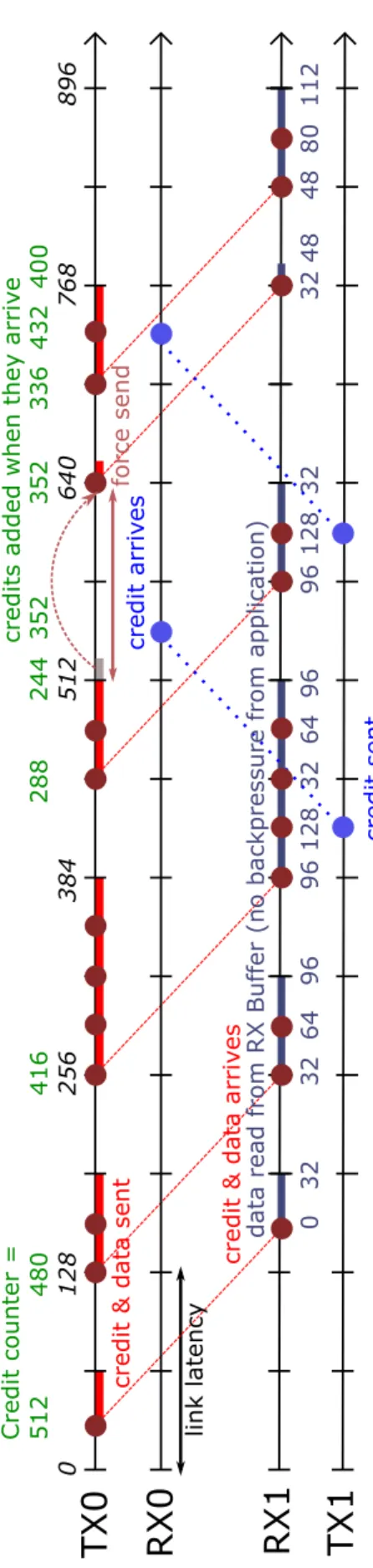
To verify the interaction between credit counter and the design parameters (TX/RX buffer allocations and CU frequency), timing diagrams are shown in Figure 2.2 and Figure 2.3. Credit counter in the transmitter (TX) is initially set to the receiving (RX) buffer alloca-tion and decrements whenever a data flit is sent. In this simulaalloca-tion, a link latency of 128
cycles is assumed. Based on Equation (2.5), the maximum DCUis set to 128 (DCU = 128),
which is equal to (TX buffer depth).
Figure 2.2 shows TX0 from FPGA 0 continuously sends data stream to RX1 of FPGA 1, where no backpressure is applied from the receiver FPGA. This implies a constant
throughput at RX1 buffer, which sends a credit every (DCU = 128) buffer reads to update
TX0 of RX1 buffer status. When credit is sent by RX1 to TX0, it takes a number of cycles (represented by the link latency), 128 cycles in this case, before it arrives at TX0, which in turn, updates its credit counter. As shown in Figure 2.2, the credit counter is always updated every 128 cycles, which implies the availability of RX1 buffer.
2.3. Results and Discussion TX0 RX1 0 128 256 384 512 640 768 896 0 128 128 128 128 128 128 arrives data sent
read from RX Buffer (no backpressure received)
link latency
credit sent
Credit counter =
512 384 256 256 256 256 256 256
credit added
Figure 2.2: Timing diagram with constant RX buffer reads (no backpressure)
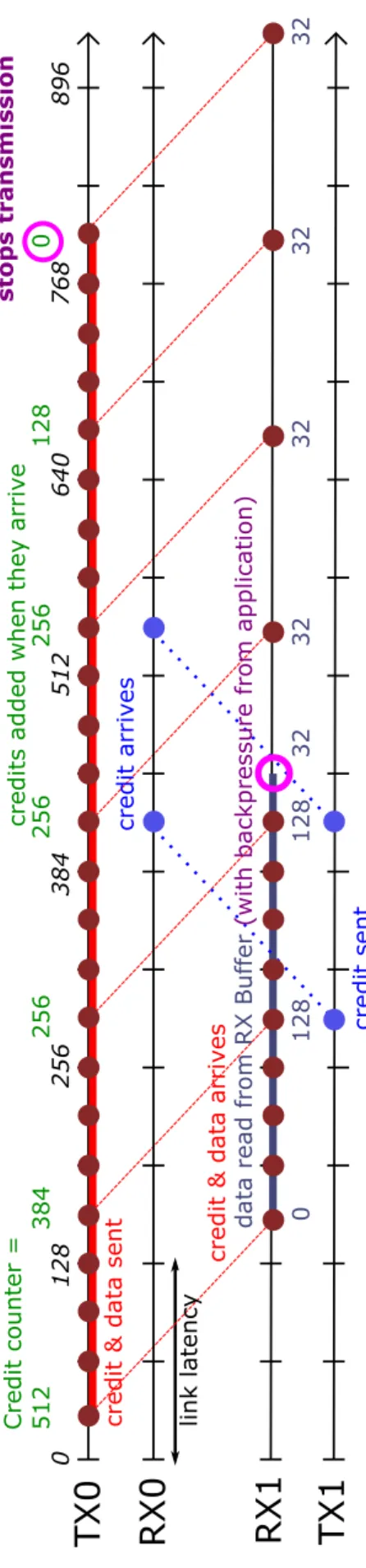
TX0 RX1 0 128 256 384 512 640 768 896 0 64 128 64 128 64 128 arrives data sent
read from RX Buffer (backpressure asserted at every other cycle)
link latency
credit sent
Credit counter =
512 384 256 128 128 0 128 0
credit added
Figure 2.3: Timing diagram with intermittent RX buffer reads (with backpressure)
Figure 2.3, on the other hand, initially shows a high data transmission rate. However, the receiving end’s RX1 buffer is simulated to receive backpressure signals at every other cycle from its application’s sink port, which reads the buffer. This causes the RX1 buffer
reads twice as long to reach (DCU= 128) compared with the other case, which delays the
sending of credits to TX0. On the TX0’s end, its credit counter eventually gets depleted due to its infrequent updates, which mimics the backpressure signal to stop transmission, as propagated from the RX1 buffer. In Figure 2.3, data transmission rate is shown to be balanced between the transmitting FPGA and the receiving FPGA. This demonstrates
2.3. Results and Discussion
2.3.2
Case Studies for Full and Half-Duplex Inter-FPGA
Com-munication with High and Low Data Transmission Rates
The interaction between the communicating FPGAs in both full-duplex and half-duplex operations are investigated in this section. Here, the same design parameters are assumed:
link latency is 128 cycles, DCU = 128, and TX buffer depth is 128.
Figure 2.4 shows a loop back configuration, where FPGA 0 sends data streams and FPGA 1 receives them, then sends it back. TX0 initiates transmission when its TX0 buffer is full. After 128 cycles of propagating the link, the header or control flit, along with a credit of the first FC packet arrives at RX1, followed by its succeeding data flits.
After DCU = 128 RX1 buffer reads, TX1 begins sending back the data streams to RX0.
For both communicating ends, the received credits are added to their respective credit counters to update the RX buffer status of the receiving FPGA. Since this case illustrates a high data transmission rate and there is no backpressure assumed from both RX0 and RX1 buffers, then continuous transfers for both directions occur seamlessly.
Figure 2.5, on the other hand, shows a low data transfer rate case for full-duplex channels, where intermittent data transfers are initiated by TX0. As with the other case, RX1 receives the incoming data streams, and transmits them back through TX1 when its TX buffer is full. No backpressure from application is likewise assumed in this case, and credits are still added as soon as they arrive. In this figure, a force send occurs when data flits occupy a TX buffer after a certain period (TX1 buffer in the figure), which guarantees the transmission of all TX buffer entries in the event that it never becomes full.
Meanwhile, Figure 2.6 shows a high transmission data rate in half-duplex data trans-fers. The same operations and interaction between the design parameters are observed
here, except that only one direction is utilized (from TX0 to RX1). After DCU = 128 RX1
buffer reads, its corresponding TX1 sends credits encapsulated in control flits to RX0, in order to update FPGA0’s credit counter. Likewise, credits are added when they arrive and since no backpressure from FPGA1’s application is assumed, then data transmission
2.3. Results and Discussion
from TX0 to RX1 is uninterrupted.
Figure 2.7 shows half-duplex intermittent data transfers from TX0 to RX1. No back-pressure is still assumed from the application in FPGA 1, so the transmission rate is balanced with the receiving rate. Sending credits by TX1 takes longer since RX1 buffer
also takes a longer time to fill and reach DCU = 128 buffer reads.
In Figure 2.8, continuous transmission is performed by TX0, in which transmitted data streams are continuously received by RX1. However, a backpressure signal is assumed to be asserted by the application in FPGA 1, where RX1 buffer reads are stopped. This eventually results to depletion of credits in TX0 since no credit updates are sent by FPGA 1, which stops TX0 transmission, therefore implying backpressure propagation from the receiving FPGA.
2.3.3
Implementation and Evaluation
To obtain the inter-FPGA link delay for FC evaluation, a prototype platform with the network modules is implemented with a Terasic DE5A-NET board [82], which has an Intel Arria 10 FPGA with four high-speed, low-latency quad small form-factor pluggable (QSFP+) transceiver links, each with 40 Gbps data rate. For this initial evaluation, a point-point connection is implemented, where two transceiver links are bundled to-gether to obtain a peak bandwidth of 80 Gbps or 10 GB/s. Here, the network modules for a direct network are considered and implemented, as shown in Figure 2.1, where point-to-point L1/L2 IP cores are utilized with FC modules on both communicating ends. In this experiment, a direct network is considered; however, the FC is universally designed to be compatible with both network types. Further discussion on the implementation and evaluation for an indirect network with an FC module is found in Chapter 4.
Based on the design parameters introduced in the previous section, the TX/RX com-munication buffer depths are selected. Figure 2.9 shows the effective link throughput when sending different data stream sizes with different TX buffer depths. For shorter data streams, smaller allocation has a higher effective throughput due to a smaller TX
2.4. Conclusions
buffering overhead. However, this overhead becomes negligible in longer data streams, where the three different buffer depths converged to an effective link throughput of 7.92 GB/s. Since the target is for a generalized FC design, TX buffer depth is set to 32. Mean-while, point-to-point link latency is 365 ns, which is 82 cycles at F = 225 MHz. With
this, Dlink = (82) + (32) + (4) = 118 cycles (see Equation (2.2)), where TX buffer depth =
32 and RX buffer write-forward = 4 cycles. RX buffer depth = 512 is selected, which is
sufficiently larger than (118 × 2) + (32) = 268 (see Equation (2.2)). Here, DCU = 32 cycles
and is a statically chosen interval that satisfies Equation (2.4).
Figure 2.10 shows possible design parameters, where as expected, the network modules
with TX buffer depth of 25 = 32 and RX buffer depth of 29 = 512 consume the least
resources with only about 1.12% of the internal memory resources (Kbits), indicating a tiny footprint.
For an indirect network, it is expected that the link latency is slightly higher than the point-to-point’s, due to the switch. In this case, TX buffer depth and CU frequency may be kept constant for both networks; however, the RX buffer may need to have a larger allocated size. This is further discussed in Chapter 4.
2.4
Conclusions
This chapter presents a lightweight and efficient hardware backpressure mechanism for inter-FPGA communication in direct and indirect networks, which is required for certain applications such as stream computing. This is achieved through a general-purpose hard-ware design of a credit-based flow control mechanism for communicating FPGAs, which results to a custom network protocol for additional reliability. The flow control design handles both synchronization, which ensures both communicating FPGAs’ active status, and the sending of credits, which serves as backpressure mechanism for receiver status awareness. Furthermore, flow control autonomously supports half-duplex and full-duplex transfers.
parame-2.4. Conclusions
ters of flow control mechanism were identified and explored. A point-to-point inter-FPGA connection is implemented with network modules, including flow controllers for both ends. Important design parameters such as the TX and RX buffer depths are evaluated in rela-tion to performance and area consumprela-tion. For the store-and-forward TX buffer, which is equal to the credit update frequency, sufficient depth is necessary to reduce transmis-sion overhead while minimizing additional latency. The RX buffer depth is based on the actual inter-FPGA’s TX-to-RX link latency and must be more than its round-trip time and credit update frequency to allow high link utilization and reduced transmission time. However, it should have a minimum depth to allocate more area for the application. Equations (2.2), (2.3), and (2.4) summarize these important relationships. By utilizing the design parameters with the least resource utilization, the network link throughput averages at 7.92 GB/s.
Although the evaluation of the flow controller module is through the implementa-tion and investigaimplementa-tion of design parameters in a direct network, the same concepts follow for an indirect network. With a longer link latency, it is expected that the flow con-troller’s RX buffer allocation for an indirect or switched connection will be larger than the point-to-point’s (direct’s), which affects area consumption. This is investigated further in Chapter 4.
2.4. Conclusions
TX0
RX1
0 12 8 25 6 38 4 51 2 64 0 76 8 89 6 credit & data a rri v es link l atency credit & data s ent Credi t counter = 512 384 256 256 256 256 256 credits added when they a
rri v e
RX0
TX1
credit & data s ent data r ead fro m RX1 Buffer ( no backpr essure fr om appl icat ion) credit & data a rri v es Credi t counter = 512 384 256 256 256 256 credits added when they a
rri v e data r ead fro m RX0 Buffer ( no backpr essure fr om appl icat ion)
2.4. Conclusions
TX0
RX1
0 12 8 25 6 38 4 51 2 64 0 76 8 89 6 0 32 32 3 2 32 32 3 2 32 32 3 2 16 32 link l atency credit & data s ent Credi t counter = 512 480 416 288 244 352 352 336 4 32 4 00RX0
TX1
force send credits added when they a
rri v e credit & data s ent credit & data a rri v es credit & data a rri v es Credi t counter = 512 384 416 384 416 416 448 480 4 48 credit
s added when they a
rri v e data r ead fro m RX1 Buffer ( no backpr essure fr om appl icat ion) data r ead fro m RX0 Buffer ( R eady = al w a ys 1) 0 32 32 3 2 32 32 3 2 32
![Figure 1.1: Critical Areas for FPGA Research Identified by Underwood et al. [1]](https://thumb-ap.123doks.com/thumbv2/123deta/5908070.1050000/18.892.119.788.162.461/figure-critical-areas-fpga-research-identified-underwood-et.webp)
![Figure 1.2: HPC architectures over time (November 2019) [2]](https://thumb-ap.123doks.com/thumbv2/123deta/5908070.1050000/20.892.108.792.158.543/figure-hpc-architectures-time-november.webp)
![Figure 1.4: Classification of Interconnection Networks [3]](https://thumb-ap.123doks.com/thumbv2/123deta/5908070.1050000/31.892.124.757.211.1097/figure-classification-of-interconnection-networks.webp)