科学技術・学術政策研究所 講演録―297
SEMATECH における研究とイノベーション戦略
米 SEMATECH 副所長 Raj Jammy
2013 年 12 月
文部科学省 科学技術・学術政策研究所
科学技術動向研究センター
本講演録の引用を行う際には、出典を明記願います。
本講演録は、2013年3月15日に文部科学省科学技術政策研究所で行われた、SEMATECH 副所長 Raj Jammy氏の講演会の内容を、講演者の了承のもとに当研究所においてとりまとめたものである。
また、本講演録の内容は、講演の記録として講演者の見解を掲載しており、当研究所の公式の見解を示すも のではないことに留意されたい。
編 集 : 文部科学省 科学技術・学術政策研究所
科学技術動向研究センター 市口 恒雄 客員研究官
問合せ先 : 〒100-0013 東京都千代田区霞が関3-2-2
文部科学省 科学技術・学術政策研究所 科学技術動向研究センター TEL:03-3581-0605 FAX:03-3503-3996
科学技術政策研究所講演会
演題: 「SEMATECHにおける研究とイノベーション戦略」
講師: Raj Jammy (SEMATECH 副所長)
コメント: 鳥海 明 (東京大学教授)
日時: 2013年3月15日(金) 15時00分~17時00分
場所: 新霞が関ビルLB階 201D号室 科学技術政策研究所会議室
言語: 英語(質疑応答は日本語でも可能 )
講演趣旨:
1987年に米国で発足した官民共同による半導体製造技術組合SEMATECH (SEemiconductor MAanufacturing TECHnology)は、米国の半導体産業の競争力回復に成功を収めた。その後は、
米国以外の半導体会社も加わり、国際的な半導体研究の拠点になっている。現在も、紫外線露光 による微細化プロセスや3次元配線などの先端的な研究で、世界の半導体研究をリードし続けて いる。そして米国におけるナノテクノロジー産学官連携拠点であるAlbany Nano Tech Complex においても中核機関としての地位を確立しており、コンソーシアムマネジメントの観点からも重要な 存在となっている。
このような官民共同のコンソーシアムを大きな成功に導く秘訣は何か、そしてそのマネジメントや 組織はどうあるべきかを、マネージャーの立場からお話を伺う。
講師経歴:
SEMATECHの材料および技術融合担当副所長。特に、革新的スケールで技術を融合する研
究の責任者を務める。過去4年間は、フロントエンド・プロセッサー部の部長を務めた。
IBM社の半導体研究開発センター(East Fishkill, NY)で、デープトレンチDRAMのフロントエンド 技術の開発に従事した後、DRAM開発組織の熱プロセスと表面処理グループの責任者となる。
2002年に、ワトソン研究センター(Yorktown Heights, NY)に転勤、high-k誘電材料ゲートの開発責 任者となる。
米国ノースウェスタン大学で博士号を取得し、50件以上の特許の取得と150件以上の論文発表 および講演の実績を持つ。
(本講演後、4月よりIntermolecular Inc. 半導体グループ担当副社長)
講 演 内 容
SEMATECH における研究とイノベーション戦略
Raj Jammy (SEMATECH 副所長)
【司会者】 それでは、定刻になりましたので、科学技術政策研究所所内講演会を開催さ せていただきたいと思います。本日は、お忙しい中をお集まりいただき、ありがとうござ います。司会進行をさせていただきます市口と申します。お手元に資料が3枚ありますが、
もし足りない方がおられましたらご挙手をお願いします。
本日は、世界的な半導体研究の拠点でありますSEMATECHのJammy副所長をお招き して、ご講演をして頂くことになっています。本来なら、この講演会の講演趣旨と講師の 方のご経歴をご紹介しておりますが、お手元にお配りしております案内状に記載しており ますので、詳細はそちらを読んでいただくことにして、説明は省略させていただきます。
時間配分は、Jammy先生のご講演が約60分、それに続いて東京大学の鳥海先生のコメ ントを約10分間いただくことになっております。その後30分ほど質疑応答、あと残り20 分ほどを名刺交換のために時間を残しておきたいと思っています。
それでは、早速、講演をお願いいたします。
【Jammy】 Thank you very much, Ichiguchi-san. Good afternoon, everybody. Thank you for joining me here today. It is my pleasure to be here at your office, NISTEP. I also want to thank Ichiguchi-san and Kamiyama-san and Chuma-sensei for the invitation to come to Japan and to present some of our works, how we collaborate at SEMATECH and why collaboration is critical in our opinion. And to me the discussion that we have today is more around how future of research and development must be done and how it is necessary to be done, as we go into many complex situations in the coming years. This is probably example of
semiconductor technology, but the same example can be applied in many other fields.
To take this discussion off, I would like to go through semiconductor industry, how the industry has grown and what scaling is all about, and I
also talk a little bit about Fig. 1
the industry’s current trends and some gaps between the R&D costs and revenue in the semiconductor industry.
That may give you an idea of why a collaborative organization like SEMATECH makes sense, how SEMATECH was established and what is the impact of that. What are the major transitions that are taking place in the industry?
The semiconductor industry
is continuously going through changes and transitions. It is important to look at that change and transition today. And of course, Toriumi-sensei is a big part of some of these changes in the industry; some of his research directly impacts many of the things that I’m going to talk about today.
At the end of this presentation, I would like to highlight some of the discussion topics that we go through as a summary point. What I would like to do is to talk about what makes a consortium successful, why a consortium can be successful and what is necessary for that.
Now, through all this presentation, please stop me if I am speaking too fast. I speak very fast, so please stop me and tell me to slow down.
So, let’s start with the first topic: semiconductor industry growth (Fig. 3). In the semiconductor industry, we have what is called a virtuous cycle (Fig. 4). We call it virtuous because we innovate, and that innovation leads to new technology, and that new technology obviously is giving us lower cost and more functionality. Once we have a virtuous cycle, we have more applications, business increases, and then obviously revenue is going up. So once there is more revenue, again we invest it back in R&D, and more ideas, more innovation, and we continue. This is how we have been doing for a
Fig. 2
Fig. 3
long time. Although this is called a virtuous cycle, this may be a dangerous cycle in one way. The danger comes because the need for R&D and the cost of R&D are continuously increasing.
Unless the application space is expanding faster, you would not gain an advantage from the virtuous cycle. You will see that during the presentation.
No person in the
semiconductor industry can do a presentation without talking about Gordon Moore. I am from the semiconductor
industry, so I have to tell you about Moore’s Law (Fig.
5). I am sure that many of you are familiar with Moore’s Law, so I do not have to spend too much time here. Just I want to make one very important point: Moore’s Law is neither a technology law nor a scientific law. It is purely economics. When
the number of transistors is doubled, the designers can put more circuits on the same chip. More circuits mean more functionality. Therefore, the customers and consumers are happy that the next-generation cell-phone can do more work and the next-generation laptop can be faster. At the end, that is literally what has been happening.
Right here, I want to say “If we can get this kind of functional improvement by other methods, it is also good.” I think the industry is going in that direction. I was talking to Kamiyama-san a little before, and both of us believe that conventional scaling
Fig. 4
Fig. 5
approaches may not be necessary. Some of the ideas that are being looked at today might be more appropriate for future generations. If we select materials that are pioneered by various groups, a lot of non-lithography techniques might be the direction that we should look into. We will come back and talk about that subsequently.
For those of us in the room here who might want to get an idea of what kind of semiconductor technologies and how the scaling happened, Fig. 6 might be of an interesting chart. In 1970s, when the Intel’s first chip 4004 was introduced, the number of transistors was about 2,300. That means it is like an auditorium or a hall. In mid-1980s, when Intel 286 was introduced, the capacity in terms of transistors was about 134,000 just like a stadium. By the time when Pentium III was introduced, the number of transistors went up to 32 million, which is like the population of Tokyo. Now, we have 1.3 billion transistors, and some of the chips that are being made today are close to 2 billion transistors. The number of 1.3 billion is equaling to the population of China. If transistors were people, this is how you would see them. You can imagine the size of these data.
What is interesting is that actual chip size has not changed. I think this is probably the most important thing in the industry. The chip size has to remain the same as back in 1970s. In reality, what we have is the population of China on a chip. That is really the scaling power that we are all working on today.
Now, another very important factor within the Moore’s Law is that we are getting lower and lower cost. Figure 7 shows the cost per transistor and per frequency. The frequency is a typical measure for performance improvement, in general. So far, that is how the industry has been looking at it. From that perspective, there is a significant reduction in terms of cost as being scaled. You have not only been able to put more
Fig. 6
transistors in a chip by making them smaller, but also you have been able to reduce the cost per transistor as well at the same time.
Now, let’s start looking at technology trends and industry trends and where are the gaps (Fig. 8). The big driver was a personal computer in 1990s, and PC was a big thing (Fig. 9). Everything was made for PC and everything was geared around PC. In 2000s, it was on Internet. The computer
was important, but how fast the computer was be able to get the Internet information was more important than the computer itself. Today, it is more about smart technologies. By smart, it is not just a technology being smart; it is more about how the technology interacts with us. It
Fig. 7
Fig. 8
Fig. 9
may be more about people than about the technology itself. What is required to be smart is very important.
In the past, we had display technology, computing technology, communication, storage, sensing, and all separate technologies. Today, it is not the case; they are all integrated. We have functional integration in
these technologies. If we look into how this is doing, we are putting all these technologies together so that we have a higher level of functional integration, and we can access information wherever we want, whenever we want, and whatever information we want. We may access the entire collection from Library of Congress or the entire scientific database may be available in our pockets. That is the direction we are headed. This is an important change we are seeing right now.
This trend is also related to some other changes that are coming in mobile computing platforms and mobile communicating platforms (Fig. 11). Mobile communications and mobile computing are coming together. At the same time, the growth rate for mobile communication platform is very fast (see Fig. 11). In fact, the demand is so much higher
for communication chip that the supply cannot match. It is expected to be the same way for the next few years. It is also important that these computing platforms always have a communication part attached to them. That is why these two are coming together. Similarly, behind
Fig. 10
Fig. 11
every cell-phone, there are cellular technologies. This means that cellular technology is also growing very rapidly.
Now, the new technologies’ needs are very different. In case of communication technologies, main important thing is low and ultra-low power technologies. You need ultra-low power devices and cell-phones. Even cloud computers also need low power technology because the number or the size they have to deal with is so huge that they need a power plant right by the side of a server station. It will be expensive. In fact, Google started their server station by Columbia River in Oregon State only because there was a power plant right next to it. They need that much of energy just to run a server station today. Therefore, the low power is very important.
Second important thing is memory technology. Dense memory is another absolute need. We all create a lot of information on a daily basis. All the information is not just created, but it is also stored. In some cases, the information may be multiplied many times and saved. For example, university degrees, health records, benefits, and financial reports are kept in different locations multiple times. If we are going to store such information for the entire lifetime or if people create one’s own information, we have to think about how to save it. How much memory each person would have on the planet? We have 7 billion people today, and from today standard, each person may consume 10 terabytes of information through the entire life. Information of seven billion times 10 terabytes are a huge load of memory.
We talked about function integration in the previous part (see Fig. 10), and it means more companies are coming together. There is a large problem when we use the fast logic and high-density memory: How fast do we send information from the logic to memory? And how fast do we take it from memory storage and send it to the logic when we need it? The communication channel becomes a very important piece. Namely, the fast data transfer between the modules or between the chips is a very important thing.
All these things have significant gaps. This is what the industry wants, but I do not think that it is possible today. We need some new revolutionary changes in the device technology. I will come back to that later, but I want you to hold that in your mind.
Now, I would like to show you how ITRS, the International Technology Roadmap for Semiconductors, is treating the same thing (see Fig. 12). One direction is, of course, the Moore’s Law direction, and the other one is functional diversification of more than Moore’s Law or beyond Moore-based technologies.
Now, in this situation of course, one can continue to scale; that is one possibility. But, there is another possibility where you can continue to add more functional components on the same chip. This is called “system on a chip” or “system in a package.” I will talk about that piece. Adding different components on
one chip has a big advantage because it means that we get more scaling indirectly. It is equivalent to the ordinal scaling that was done with dimension shrinking. Thus, higher value systems using “system on a chip” or using “system in a package” is a new direction the entire industry is going.
I talked about gaps and about changes, and those changes are here (Fig. 13). The device evolutions or technology evolutions are listed up in Fig. 13. There are very important things in three categories. The first category is that most devices are going
Fig. 12
Fig. 13
towards 3-dimensional devices. We are no longer making devices on a flat surface, but we are making 3-dimensional structures. Scaling itself is going to take advantage of 3-dimensional structures now. Next important piece is that a lot of new non-silicon materials are coming out both for logic and for memory.
We need electrons in a memory device in order to store a piece of information. The current memory technologies, however, do not store enough electrons. We have about 10 electrons in each memory cell. The 10 electrons are not good enough statistically to ensure that we can come back and access the information after one year. That is a big issue. Another important part is low power. Because of low power or ultra-low power technologies, we may not use CMOS, but we may use something different technology. It is another important change that is coming up.
The next changes that we should be looking into are the System-On-a-Chip and System-In-a-Package, which we talked earlier. These two are also significant changes because we are putting different components on the same die. You have the same size of die, but you have a lot more functionality coming from the die. Thus, System-On-a-Chip and System-In-a-Package are new important trends.
The last one is an equipment-based change. You need the right two sets of infrastructure. Extreme UV is one area, which is extremely difficult, and there are a lot of works going on in that direction. The other is wafer size; there is a transition from 300 mm to 450 mm diameter.
Each of these things has a huge amount of works and resources that are necessary to make these changes happen. What is interesting to me is that the industry is pursuing all these changes at the same time today. In the past, even if you did one of them, it was a large change. But we are all working hard to cause all of these changes at the same time. That is the big challenge.
Now, let me talk about the cost of R&D and what is happening in the cost of R&D.
Before that, I would like to mention a little bit of the history of the industry itself. The semiconductor industry started in the United States, Silicon Valley area, 50 years ago (see Fig. 12). It was Bell Lab. that invented the first transistor. A lot of the semiconductor industry started in the Silicon Valley area, and this industry is continuing to grow faster than the GDP of the United States. The semiconductor industry is needed economically. If there is not this industry, the economy will collapse
Fig. 14
in many countries.
The annual sale in 2011 was $300 billion worldwide. That $300 billion allows for making systems that are valued at $1.1 trillion, and allows for a huge employment potential. These are very large numbers because they also have an economic multiplier factor. Every high-technology job creates 5 to 10 other jobs. Thus, the economic multiplier factor is very high in this industry. Because the semiconductor industry is a very vital component of IT, it is a growth engine for the world. In the U.S., the semiconductor industry has the largest employer with high wages. There are about 200,000 people employed in this industry in U.S. alone. Now, it is the number-one export performance industry for U.S. along with jet engines and aircraft. Eighty percent of the U.S. industry sales are outside the United States. Thus, a lot of exports come from this.
The worldwide revenue is continuing to increase. The interesting fact to me is that the ratio of R&D expense to the revenue is also going up. Very few industries can claim that they will spend 20% of their revenue for R&D. It is a necessity at the same time in the semiconductor industry.
This is probably a sign of the future and how things are going to be looked at, not only in this industry but other industries as well, biotechnology and medical technology and so on. Why is this happening? One reason why this was inevitable to happen in many industries in the past is that the industry was vertically integrated. For example,
Fig. 15
IBM, from which I came, used to make its own systems. They had their own design house where they had design teams. They had packaging and assembly plants. They also kept internally developed chip technology such as
process technology. They also made their own software tools for verification and design layout. Of course, they did not buy the equipment and materials from outside. That was before.
Today, the industry is fragmented (see Fig. 16). Since mid-90s, the industry splits up into several segments. Many companies decided to become fabless. In fact, some newly started companies were purely design-driven and fabless. They contracted manufacturing to a foundry. Memory, logic, and IDMs (Integrated Device Manufacturer) essentially became a small separate segment. Packaging and assembly became a separate segment. EDA (Electronic Design Automation), equipment, and materials became another segment with suppliers clearly being distinguished there.
Now, at the top is the system house. The companies that make systems are the ones Fig. 16
Fig. 17
that control the profits in the industry today. They do not necessarily need to spend as much money for R&D as I have shown. R&D burden is continuously getting pushed down. This is a very important change that has taken place.
Another important issue is how long it takes for a new concept to become a manufacturable idea. It takes at least ten years. Many concepts that we are using today have been looked at for almost 10 to 20 years by the universities, by research labs, or by national labs. It took a long time before they became production-worthy. There is a very long technology pipeline (see Fig. 17). It needs a long time and a lot of resources for that to happen.
Again, if each company is spending money on their own technology development in this fashion, you can imagine how much money is going to be spent in the whole industry. That is exactly what the problem is today. The semiconductor industry revenue is growing, but it is flattening out (Fig. 18). However, the total R&D cost, as a part of that revenue, is also growing. The gap, which is essentially the profit that companies make, is shrinking and reducing rapidly. That is a dangerous sign. Every company is forced to spend money on R&D multiple times. This is what needs to be addressed.
The revenue itself of the semiconductor industry is growing for a long period.
However, the revenue is becoming flat although there is a variation on the equipment side. The equipment is crucial for the semiconductor manufacturing. In fact, you cannot make chips without the right equipment.
Japan is very strong in the equipment industry. Today, the equipment industry and material supply industry are very strong in the U.S. and Japan. That is very important because we may not have to make the chips like we used to make. If the equipment
Fig.18
industry makes better equipment, it is a very controlling factor. That is a very important issue. Now, at the same time, the revenues of equipment industry are very flat (Fig 19). I will talk subsequently about how we make better equipment. I am going to come back to this topic.
Another important trend is the significant consolidation. The top-five OEMs (Original Equipment Manufactures) are supplying up to 60% of the market (Fig. 20).
Fig. 19
Fig. 20
There are five chip-making companies and also there are five equipment-making companies. Namely, the five equipment-making companies are supplying to the five chip-making companies for a $300 billion. Therefore, the risk becomes higher than ever before.
Losing some chance from a chip-making company may drive equipment companies out of business. That is a big risk factor. You can see some of these risk factors in the large year-to-year variability of revenue shown in Fig. 20, but their R&D cost has to keep up without that kind of variability. The shock is very high in the industry.
The same thing happens to the equipment sub-system (Fig. 21). When equipment companies make equipment, they need the pumps, robotics, and all kinds of sub-components that go into the equipment. The sales variability is even higher for such subsystem supplier as shown in Fig. 21. They are much more reactive; their R&D budget shakes and goes up and down almost in step with what the industry needs. This is a problem because the technology is so high-end that we need the sub-components to be much higher quality than before. If we have low quality sub-components in today’s fab, we would lose billions of dollars quickly. We have to be very careful about that.
Here, I would like to say that technologies drive our success in the industry (Fig.
22). So, how do we bring a new technology from a lab to fab? To do that, a comprehensive and industry-wide collaboration is important. The challenges are global because the industry is also global. In fact, problems cut across companies many times. To find a
Fig. 21
new technology, you need to align the material supplier and new equipment company.
Consequently, the supply chain has to be completely aligned. Eventually, they have to supply to these large companies in a very high volume. If there is no supply chain alignment across the globe, it may be difficult to manufacture.
The significant investment is also necessary for these things to be successful.
Therefore, there are many consortia in the industry today. Some of them are the large-sized consortia that are working. There are a few consortia in Japan, but I choose EIDEC (EUVL Infrastructure Development Center) specifically because it is developing very important future technologies by getting a lot of contributions from many companies.
Now, let me talk about SEMATECH itself. The need for high technology and the need for collaborative work brought SEMATECH to life. SEMATECH was established in 1987 by the government of the United States, both the defense department and the House Science & Technology Committee (see Fig. 24). They got together and put $100 million per year. The industry also started putting $100 million per year. That was the original budget for SEMATECH. It is, of course, a non-profitable consortium, and was supposed to be an experiment for five years. Today, it is 26 years old; we just finished our 25th year anniversary.
It is interesting to me that in Washington D.C, today, whenever there is a crisis in any industry, the government wants to start a SEMATECH for that industry. When we had a problem in the auto industry in Detroit in 2008, the government of the United States said, “We should start a SEMATECH for the auto industry.” It was a problem with battery technology, and the government said, “We should start SEMATECH for the battery industry.” For the solar industry, they had a similar concept.
Fig. 23
Fig. 22
I would emphasize that SEMATECH is a very successful model.
The government likes this kind of model and thinks that many industries can benefit from that model.
Personally, however, I do not believe that the same model can be applied across all industries.
They have to have the
right situation for it to be successful. I will talk about that subsequently, but that is my opinion.
Once SEMATECH was established, there was a definite impact. We saw that the industry in the U.S., which was declining, started picking up and it improved to a leadership position (Fig. 25). One of the focus areas at SEMATECH was how we improved the equipment quality and reliability in order to boost the device yield. That was the focal theme when SEMATECH was established. We saw that it had an impact and the benefit came out.
Since then, SEMATECH moved on from the initial position of serving the U.S.
industry to the next position very quickly; it became a part of the international community because the
U.S. government, as well as the member
companies of SEMATECH, realized
that this problem is not local to the United State.
This problem is global.
We have to work together with many companies in many other countries.
Fig. 24
Fig. 25
The first step was the transition to 300mm wafer size. The wafers were 200mm diameter before that, and the industry was considering to switch to 300mm. They used that as an opportunity to form the “International 300mm Initiative,” which was the first international consortium (Fig. 26). From that time, SEMATECH became permanently international SEMATECH.
Then we started looking at different opportunities. One main opportunity, which we were pursuing, is our relationship with the State of New York and the College of Nanoscale Science and Engineering (CNSE) in the State University of New York (see Figs. 26). That is our partner.
Fig. 26
Fig. 27
There are two important partnerships that we have right now. The U.S.
Department of Energy asked us to work on photovoltaics to improve the manufacturability. So we started the photovoltaic manufacturing consortium (PVMC) with the U.S. Department of Energy. There is also a work going on in 450 mm wafer size transition; G450C. Now, this whole SEMATECH model, a catalyst for the industry to develop technology, has been recognized as being quite successful.
Thus, SEMATECH is a global consortium today (Fig. 27). Originally, we had only the chip-making companies, but we have now more members from the entire industry even though the chip-making companies are the core members.
We have people from the SEMATECH Ecosystem (Fig. 28), which consists of IC fabs such as IBM, original equipment manufactures (OEMs) or equipment suppliers, and materials and substrates suppliers. We have subsystem or consumable suppliers, fabless companies, and semi-component companies as well, who become a part of this consortium. It is very important that the entire Ecosystem comes into play together at the same time. It is necessary to have everybody’s opinion because somebody else may impact the person who uses it at the end. We see that such examples are increasing.
The other important thing is that SEMATECH has a strong worldwide network among chipmakers, suppliers, universities, and government agencies including the State of New York (Fig. 29). Although the State of New York is a very important partner for us, we also have relationships with many government agencies around the world, and we have the facilities and research activities there. We work with research labs not only in the United States but also in other countries. The partnership with suppliers is
Fig. 28
also very close and dense.
More than 60 universities are also in our partnership today. We continue to expand the relationship with universities because it is important for us to develop new ideas and new research projects.
If we summarize this, I should say that SEMATECH Ecosystem is a good example of very strong partnerships
among industry, academia and government (Fig. 30). Some of the universities and national labs are listed here.
Fig. 29
Fig. 30
Let me show you where SEMATECH was started first. In 1987, SEMATECH was started in Austin. Figure 31 is a 200mm facility.
It has been sold and now it is a private facility of R&D foundry that runs over there. Of course, we continue to maintain a small presence in this facility, but most of our activities are in New York
In New York, there is a 300 mm
fabrication facility that the State of New York has built. It was necessary for us to move because we had an opportunity to make the transition to 300 mm in this core facility by ourselves (see Fig. 32). Otherwise, we could spend almost a few hundred million dollars to convert the fab to 300 mm. We were able to collaborate with other companies like IBM and the State of New York, and were able to use this facility. Thus, SEMATECH, IBM and the State of New York collaborated together to get this facility going. Today, the same office building is shared by all of us: The entire second floor is for SEMATECH, the third floor is for IBM and partners, and the fourth floor is for the university faculty.
Subsequent to the original fab, we constructed the additional fab, NanoFab 300 Fig. 31
Fig. 32
North, which has a 300 mm cleanroom, and the total area is about 228,000 square feet.
When we were constructing this fab, we ran out of space because there were too many tools for many programs at that point. We needed to construct an extension fab of 300 mm right by the side of that. Today, in fact, all three fabs are full, and there is no room to put a new tool. If we want to bring a new tool here, we have to throw something out.
When we started the 450 mm program and the EUV (Extreme Ultraviolet Lithography) program, we realized that a new facility was needed. So we needed a new building right across the street. Figure 32 is an old picture, and this new building is almost done. The total square footage available on the site today is 800,000 square feet of office space, not counting the new building. We will be adding even more space when the new building is fully functional.
There are 2,600 R&D jobs on the site today. The total investment is about $12 billion in this facility, from industry, government and others. What is also important is there are more than 250 industry partners working on this site. Now, we have many companies working with us (see Figs. 27 and 28). We also have the equipment suppliers who have established room capabilities there. That is a very important component of how this place is working today.
President Obama visited us to inaugurate the new building last year (Fig. 33), and we were all quite inspired by having President Obama there. The new building is up and running now.
I want to switch my topics and talk about SEMATECH’s program (Fig. 34). What does SEMATECH do? What do they focus on? Do they research? Do they develop something? Do they manufacture something? Those are questions that you may have.
We do not research because a basic research is not interesting for us. We do not manufacture anything because it is left to companies. What we do is the technology development. We do work a little bit with universities and national labs, so that there is applied research that is being done, and so that we understand what are the new
components coming out of Fig. 33
Fig. 34
universities and what are the promising new ideas. How do we take that idea from a lab and make it manufacturing-worthy? How do we take it to a fab?
If we have a new technology, can we just directly manufacture it? Maybe we cannot.
Do we have the right equipment? Do we have a good understanding of what kind of materials are needed? What kind of precursor is appropriate first? Do we have the right model? We want to understand liability, and we want to understand failure mechanism in these materials. There is a lot of work that happens at SEMATECH.
There are fundamental works such as basic physics and engineering. They are, however, common works, and all the member companies need the works anyway. They can do the works by themselves with spending a lot of money, or they can come to SEMATECH and share resources. Once they do that, then they can bring it back to their own company and become competitive. That is where we focus. A technology has been manufactured, and then we go there and say, “How do we make it more efficient?
Is the equipment consuming too much electricity? Is this process consuming too much water? Is there an environmental or a safety issue with these chemistries or these precursors? How can we address those things?” Those are important issues as well.
Those kinds of things are tackled by one of our groups called ISMI.
This is the comprehensive set of activities that we have (Fig. 34.). It is very important that we are membership-driven; we do not conduct these projects just by ourselves, but we get direction from the industry. They tell us, “We need this. How we
are going to put this together?” Thus, we work with them to define problems and milestones, and develop the technology. We also get consensus from the industry so that there is a common standard and common benchmarking. It is very important for us to make sure that the problems are critical so that companies cannot solve themselves. If the company can solve them alone, there is no point in wasting our resources there.
The economic impact of SEMATECH is quite large (see Fig. 35). The economic impact study was done by AngelouEconomics, an independent economic development consulting firm, in December, 2008. At that time, huge numbers were derived as a benefit because of the establishment of this consortium; $482 billion in expenditure,
$235 billion in GDP, and $141 billion increase in personal income. These are very impressive numbers. It started in Texas that was cowboy country before 1987. It was dependent on oil and ranching. That was the economy in Texas. Today the high-technology industry is the largest employer in the State of Texas. There is a proof which tells why this kind of consortium is valuable.
Let me summarize here as shown in Fig. 36. A trend in the industry is consolidation.
Both device makers and supply chain have significant consolidation. The cost of R&D is rising; very few funders can invest. The problem in the supply chain is an insufficient early feedback from the device makers. Infrastructure affordability is very expensive. A material supplier needs to have the equipment, and also needs to have the best structures that are electrically testable. Where do they get that? They are neither a chip maker nor an equipment maker. Hence, infrastructure access is very important, and the
Fig. 35
business model may be broken because of this. The R&D burden is pushed down because the cost is high for the smaller companies.
Therefore, a compelling collaborative model is necessary, and it is also important to show a clear pathway to 450 mm activity.
Now, let me quickly go through some of the technology transitions and why this is important (Fig. 38). Especially, I want to share with you the magnitude of the problem
Fig. 37
Fig. 36
Fig. 38
we are trying to deal with as we try to make these changes. In terms of wafer size, I talked about 450mm transition. In terms of device, we experienced the change in high-k and changes to FinFETs, germanium device and other new types of devices.
Interconnects are going towards 3-dimension
connections. Lithography is going towards EUV (extreme ultraviolet). Many new changes are coming and are continuously happening.
Of course, SEMATECH has been in the middle of all these changes over the years.
Our organization structure is based on those kinds of changes. Today, we have a lithography group, an interconnect group, materials and emerging technologies group, and a manufacturing group. These four groups correspond to what you see in Fig. 38. As we do some of this work, we keep a focus on what is coming in the future, but not what the industry can do today. I will explain that in a short.
From the perspective of a wafer size, we are going to 450 mm. The wafer size will become 450 mm hopefully in the next 3 to 5 years because the industry goes in that direction. The main reason for going from 100 mm to 450 mm wafer is the area advantage that reaches about 20 times (Fig. 39). You can get chips roughly 20 times more in a single
process. Thus, the productivity goes up and the cost per chip should come down quite dramatically.
This is the big advantage here.
I summarize the
programs in
SEMATECH that has
been done (Fig. 40). Fig. 40
Fig. 39
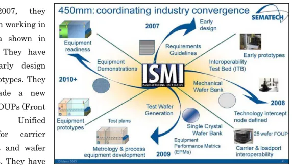
Since 2007, they have been working in this area shown in Fig. 41. They have found early design and prototypes. They have made a new type of FOUPs (Front Opening Unified Pods) for carrier transport and wafer transport. They have also interoperability
test bed. They have looked at many issues, and that is very useful for the industry, although it is not enough.
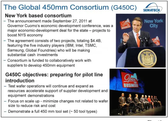
Because it was not enough, there was a big gap (Fig. 42). We told the industry, “Now you need to take this information and put it into a new consortium where you have to put more resources to build that consortium. What you really need is a new fab with 450 mm.”
That takes a billion dollars at least, but SEMATECH does not have the budget. It is the industry’s job to do that at this point. That is exactly what they are doing in G450C (the Global 450mm consortium—see Fig. 43). That was started by the governor of New York as shown in the photo. You can see all the company heads are sitting here in the second photo. Heads of Intel, Samsung, IBM, Global Foundries, TSMC and other companies are there.
Fig. 42 Fig. 41
Fig. 43 The next big challenge is lithography (Fig. 44). Lithography scaling has been continuously pushing down in terms of wavelength. Today the goal is a 13.5 nm wavelength. To make that happen, we have to do many things together.
I will show you what that is. What I want you to keep in mind is that these changes
Fig. 44
are very difficult but evolutionary. If you think about the physics, it is a very natural progress. In terms of readiness, however, the technology is not completely ready (Fig.
45). The resist resolution, the reticle protection, and the optics quality have improved quite a bit. It is probably ready for manufacturing in these three aspects, but the source power is very poor; therefore, the throughput is low. The mask capability is also not very good (see Fig. 45), and we cannot make defect-free masks today. Even if we have an EUV tool, we cannot use it still because the mask technology has to improve. There is a
Fig. 45
lot of work that needs to be done in this area.
There is a big gap here (Fig. 46). That is why we started a group called EUV EMI that focused on mask inspection technology (see right side in Fig. 46). The resist technology has also a problem (Fig. 47). If you want to do lithography, you need to have the right-quality resist. The problem for resist suppliers is that they cannot access the EUV equipment. It is very expensive and costs more than $120 million. Rather than having the equipment to buy it, we put the equipment together in Albany; both a large
Fig. 47
Fig. 48
Fig. 49 exposure tool and small micro-exposure tools. We allow them to come and work with us so that they can take advantage of this and develop the resist formation.
EUV and 450 mm are the two technologies I just talked about (Fig. 48). I want to say that these two technology changes are very evolutionary; it is a very natural change.
This is what we do. To manufacture these technologies, however, we need a revolutionary approach because they are difficult in terms of new physics and cost. We have to take a completely different approach.
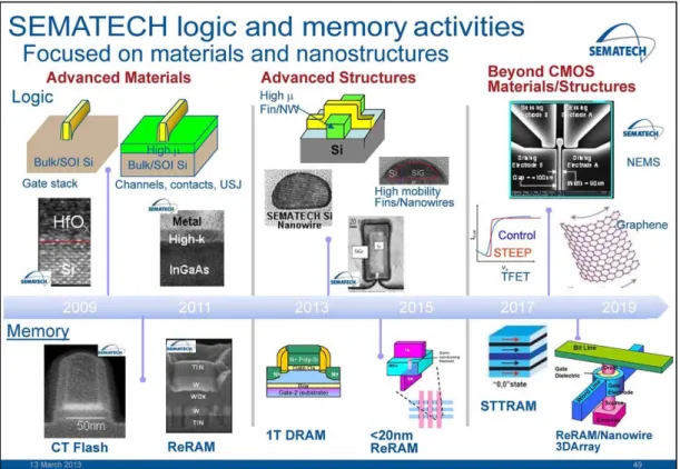
Let us move on to the devices (Fig. 49). We have a lot of activities in both memory and logic devices, focused on advanced materials. We also have activities focused on advanced structures such as Fin-FETs, nanowire FETs, and quantum FETs. This is very common; many companies do that, too. Although some of these structures will be used at least two generations ahead, we also keep focus on what might be coming in the future. We have focused also on Graphene, NEMS-based devices, and tunneling transistors (see Fig. 49). This is important to us because some of these technologies, which are called “beyond CMOS”, quickly start moving into CMOS technology area, examples being nanowire FETs or Fin-FETs. The industry has to watch when that transition takes place and we need to drive it in the industry.
There is a large change that is coming up. As we make this change from planar device to non-planar Fin-FET-like devices, there is quite a big challenge. Intel introduced these technologies two years ago (Fig. 50), and the entire industry is trying to make the same change.
Some roadmaps for the industry today are firmly 3-dimensional (Fig. 51). On the roadmap, we see also that we are going towards germanium CMOS. In the germanium
Fig. 50
Fig. 51
CMOS works, there are a lot of excellent works that have been done by Prof. Toriumi and his team. We are hoping that the industry will actually introduce germanium CMOS within the next two years or so after a 3-dimensional device Fin-FET.
Subsequent to that, the III-V device will come probably along with the germanium device. That will be another Fin-like device like III-V TFET. If we go beyond that, we believe that we have to have a new type of device like a quantum tunneling transistor or 2-dimensional graphene device.
A quite big change will be coming up in the next 10 or 15 years. This change has to be managed carefully because we need to understand exactly where the applications are and what the trends are. If we just take Fin-FETs, there are many different Fin structures that we can make at SEMATECH. Every option of structures has pros and cons, and it may not necessarily be the right structure for a particular device. In the case of nanowires, we can make stack nanowires and put all kinds of structures there.
However, each structure has many issues. Thus, we will have advantages and disadvantages.
Even in memory technology, the memory has become 3-dimensional today, and Toshiba has pioneered the biggest memory. A three-dimension is a very important concept because the industry can scale at the small cost without scaling physical dimension by lithography for the first time. The small cost scaling is the direction the entire industry will be going in the near future.
The other important part is new materials. New materials are rapidly introduced into these technologies. However, I think there is a big gap. We do not have the right
Fig. 52
materials, and we do not know how to make these materials. All these materials have to be put on top of silicon at present (Fig. 53). We cannot use other material independently.
We have a center that has focused on all these areas of the next-generation devices (Fig. 52). Again, the challenge here is that a revolutionary manufacturing technology is necessary to make a new type of memory, a new type of Fin-FET, a nanowire FET, a III-V material FET, or a germanium FET (Fig. 53). We do not have the well-suited tools today. We need to bring many new technologies in ALD, CVD, and RIE, understanding Fig. 53
Fig. 54
the physics behind them. We do not have these technologies. Ideas are revolutionary, but we need to put resources to make the revolutionary manufacturing possible.
The last area of new technology trends is System-on-a-Chip (SOC) as shown in Fig.
54. The other important part is System-in-a-Package (SIP), where we are stacking memory and logic chips together. Stacking memory and logic chips enable high bandwidth (or high speed) and low power (Fig. 55). It is also a very cost-effective solution. In this technology, Samsung has been working very hard. They have shown that, if we stack the chips together, we can get a 35% improvement in package size and 50% improvement in power consumption. The memory bandwidth or speed goes up by 800%. It is a significant improvement in bandwidth, which is important for many systems today.
A lot of attention for 3D interconnection is received by the industry. We are working in this area as well, but there is also a big gap there because many things are immature in that area (Fig. 56).
Fig. 55
Standards for 3D technology are very important (Fig. 57). We are trying to help all the companies that have an interest in this technology, and try to establish standards.
Those who define the standards are the people who would also define the technology tomorrow. This is a very important activity.
Of course, all this leads to more heterogeneous integration systems as shown in Fig.
58 down the road, but I do not want to spend time on that. Again, here is the problem Fig. 56
Fig. 57
(Fig. 59). We need revolutionary changes to make these technologies happen. A lot of researches are necessary in each of these areas for them to be successfully manufactured. We are not at the stage.
One new area that is also coming up quickly is the 10 nm size device (Fig. 60). The Fig. 58
Fig. 59
device that we make today is a 20 nm size.
The problem is that defect detection is only possible for 20 or 30 nm at best. How do we find a defect smaller than 10 nm?
We cannot see such a nano-defect that causes a heavy damage on the 10 nm
size device. Thus, the economic model of the industry would fail if you do not know how to do that (Fig. 61).
Fig. 60
Fig. 61
If we want to find a 20 nm defect on a 300 mm wafer, it is like finding 150 mm wafer in the entire country of Japan (see Fig. 62). If we go into the space and then ask someone, “Tell me where the 150 mm wafer is kept in Japan,” it becomes extremely challenging. We need to do something in this area. One example of this is our vacuum chamber. We saw a lot of carbon-based 100 nm particles on the wafer when we were using a standard O-ring (Figs. 61 and 63). We went to the O-ring supplier and told them,
“We have a problem. Can you fix it?” They said “Okay. No problem,” and came back to give us a new silicon O-ring. But we found that there were many 20-40 nm silicon
Fig. 62
Fig. 63
particles. 100 nm particles have gone but there are many 20 nm particles (Fig. 63).
A decrease of nano-defect is important. We need to understand how to fix this problem. The problem may not be the tool itself but may be in the subcomponents although we have not worried about this. If we make a 90 nm device, this may not matter that much. But this is a crucial issue when we start making 20 nm devices.
There are ESH (environment, safety, and health) implications (see Figs. 64 and 65) in manufacturing issues and metrology techniques. A whole range of issues is being
Fig. 64
Fig. 65
looked into on the manufacturing side.
One important thing at SEMAEC is the interaction between suppliers and integrated device manufacturers (IDM). It happens that one IDM interacts with many suppliers, and they communicate with each other (see Fig. 66). This is multiplied many times.
Suppliers get different inputs from each of IDM. The inputs may be neither consistent nor standard because each IDM will have different priorities. There is only limited information shared among suppliers. This causes a lot of confusion in the industry. Suppliers cannot understand where they should invest for the future, if Intel, IBM and Samsung tell them different things.
The consortium-like model is very useful because all of them sit together and discuss about what a problem is and what will be needed (Fig. 67). If suppliers focus on the area of specialty, they will get a better answer. All of them can save money and everybody benefits on that.
If they need, they can bring it to universities or national labs to work with them.
They can also bring it to other consortiums to collaborate. This is a model that is very efficient, and we have used this in many areas. I believe this kind of structure is absolutely needed in order to develop all the new technologies that I showed you. I want to emphasize that these consortiums are not limited to any specific country, specific region or specific industry. It is global. We have to work globally, and we are doing that in the semiconductor field.
Fig. 66
Fig. 67
In the last few minutes, let me summarize the success factors of the consortium (Fig. 69). If you look at the consortium itself, the success factors are its industry-led model and the clear mission. What are we doing in the consortium? That is a very important factor. Another important factor is the leadership that comes from the industry. The industry should say, “I need this technology. I want to do this. It is the important problem to solve.” The industry should also recognize that it is not a tomorrow’s problem, but it has to be long-term. A tomorrow’s problem is the proprietary problem that they have to solve internally: product development is not a consortium activity but a confidential activity. Our task has to be done in a longer-range fashion. It is the way that we can save cost. It is also important to include the entire eco-system. It cannot be just for chipmakers nor equipment and material suppliers; it has to be a broad-based ecosystem-driven activity.
It should be noted we cannot always this consortium model to other industries. The industry has to be mature and has to have enough revenue to support the consortium. If the industry is very small for some new technology that might be coming up, it does not
Fig. 68
Fig. 69
make sense to have a consortium.
I feel also that it is very beneficial to drive everybody to come together and form a consortium if there is a crisis in that industry; otherwise there is a less incentive for companies to decide that they sit together and work with other companies. A crisis is the necessary factor in some ways. It is also important for both government and industry funds to be working together.
Engagement of all the participating members is very important. They need to engage actively with the consortium because what they are doing is for the industry and for member companies. Another extremely crucial factor is agility. They should respond agilely to any changes that may be happening in the industry. If we start a project today, it may not make sense six months later. We should stop the project and look at the new activity that is necessary, rather than trying to continue the project with wasting our time and money.
Partnerships have to be global, and the business of $300 billion is global. Without the global partnership, we cannot come across the right ideas. If partnerships are not global, you do not get the right material quality, the right equipment quality, and the latest technology that is necessary. Eventually, the customers are also global. We need to be able to provide solutions in a global fashion, and that is the reason why partnerships should be global.
Now, I want to extend the summary here (Fig. 70). I have shown that the cost of R&D and the affordability of R&D are going up dramatically. The collaboration is the only answer to that. In particular, a global collaboration enables affordable R&D so that they can continue to keep pace with the development cycle of the technology.
Fig. 70