昇圧レギュレータ
NCV5171/73 製高率 1.5 A
集積蔵
280 kHz/560 kHz
、 2.7 30 V 広!"#電$範%&'() 設計柔軟性*高!+昇$,- .、順方/0転 SEPIC 123452電源構成&' () 電流6789:.;採用 (負荷4-<=安定>?@電流A限=
B実用的1方法実現高C波&'4高集積 D路組EFGH4IGBJKL.M1電源NO PQ実現()D路設計R正電$安定=
BC波数S期P;MTU>?@,V7.1 2諸機能R対対策*W))
LT1372/1373 4XY換
特長
•
集積LZ :1.5 A [証
•
広!"#範%:2.7 30 V
•
高C波&'部小\実現•
最小数]^_部•
容易1]部S期•
過電流[護蔵• C波数,`a7.R?bJ過電流状態部R対 M c減
• d :OP ^IefaP;MTU
• P;MTU電流: 50 m A *最g
• LT1372/1373 4XY換
• NCV 始)製番h特有工i>?@j更管理必要4 車載>?@kl用途R対応
♦
−40 ° C 125 ° C
•
鉛,O517xE = Specific Device Code x = 1 or 3
A = Assembly Location L = Wafer Lot
Y = Year
W = Work Week G = Pb−Free Package
SOIC−8 D SUFFIX CASE 751
VCC SS
1
517xEALYWG
8
AGND Test
PGND FB
VSW VC
MARKING DIAGRAM AND PIN CONNECTIONS
Device Package Shipping† ORDERING INFORMATION
NCV5171EDR2G SOIC−8 (Pb−Free)
2500 Units / Box
†For information on tape and reel specifications, including part orientation and tape sizes, please refer to our Tape and Reel Packaging Specifications Brochure, BRD8011/D.
NCV5173EDR2G SOIC−8 (Pb−Free)
2500 Units / Box www.onsemi.jp
+
NCV5171/73
1
2
3
4 5
6 7
8 VOUT
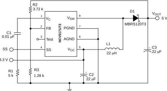
L1
5 V
C3 22 mF VC
FB Test
SS VCC
AGND PGND VSW
+
MBRS120T3 D1
22 mH
C2 22 mF R3
1.28 k 3.72 k R2
C1
SS 3.3 V
R1 5 k 0.01 mF
Figure 1. Applications Diagram
MAXIMUM RATINGS
Rating Value Unit
Junction Temperature Range, TJ −40 to +150 °C
Storage Temperature Range, TSTORAGE −65 to +150 °C
Package Thermal Resistance Junction−to−Case, RqJC Junction−to−Ambient, RqJA
45 165
°C/W
Lead Temperature Soldering: Reflow (Note 1) 260 Peak
(Note 1) °C
ESD, Human Body Model 1.2 kV
Stresses exceeding Maximum Ratings may damage the device. Maximum Ratings are stress ratings only. Functional operation above the Recommended Operating Conditions is not implied. Extended exposure to stresses above the Recommended Operating Conditions may affect device reliability.
()
!"#$%&'()*+,!-./
012 )*345/06()78#9*,!":;$-./012 )*%&*<頼=響 !"#$
1. 60−180 seconds minimum above 237°C.
MAXIMUM RATINGS
Pin Name Pin Symbol VMAX VMIN ISOURCE ISINK
IC Power Input VCC 35 V −0.3 V N/A 200 mA
Shutdown/Sync SS 30 V −0.3 V 1.0 mA 1.0 mA
Loop Compensation VC 6.0 V −0.3 V 10 mA 10 mA
Voltage Feedback Input FB 10 V −0.3 V 1.0 mA 1.0 mA
Test Pin Test 6.0 V −0.3 V 1.0 mA 1.0 mA
Power Ground PGND 0.3 V −0.3 V 4 A 10 mA
Analog Ground AGND 0 V 0 V N/A 10 mA
Switch Input VSW 40 V −0.3 V 10 mA 3.0 A
ELECTRICAL CHARACTERISTICS (2.7 V< VCC < 30 V; −40°C < TJ < 125°C unless otherwise stated)
Characteristic Test Conditions Min Typ Max Unit
Positive and Negative Error Amplifiers
FB Reference Voltage VC tied to FB; measure at FB 1.246 1.276 1.300 V
FB Input Current FB = VREF −1.0 0.1 1.0 mA
FB Reference Voltage Line Regulation VC = FB − 0.01 0.03 %/V
Positive Error Amp Transconductance IVC = ±25 mA 300 550 800 mMho
Positive Error Amp Gain (Note 2) 200 500 − V/V
VC Source Current FB = 1.0 V, VC = 1.25 V 25 50 90 mA
VC Sink Current FB = 1.5 V, VC = 1.25 V 200 625 1500 mA
VC High Clamp Voltage FB = 1.0 V; VC sources 25 mA 1.5 1.7 1.9 V
VC Low Clamp Voltage FB = 1.5 V; VC sinks 25 mA 0.25 0.50 0.65 V
VC Threshold Reduce VC from 1.5 V until switching stops 0.6 1.05 1.30 V
Oscillator
Base Operating Frequency NCV5171, FB = 1 V 230 280 310 kHz
Base Operating Frequency NCV5173, FB = 1 V 460 560 620 kHz
Reduced Operating Frequency NCV5171, FB = 0 V 30 52 120 kHz
Reduced Operating Frequency NCV5173, FB = 0 V 60 104 160 kHz
Maximum Duty Cycle NCV5171 90 94 − %
Maximum Duty Cycle NCV5173 82 90 − %
FB Frequency Shift Threshold Frequency drops to reduced operating frequency 0.36 0.40 0.44 V Sync/ Shutdown
Sync Range NCV5171 320 − 500 kHz
Sync Range NCV5173 640 − 1000 kHz
Sync Pulse Transition Threshold Rise time = 20 ns 2.5 − − V
SS Bias Current SS = 0 V
SS = 3.0 V
−15
−
−3.0 3.0
− 8.0
mA
Shutdown Threshold − 0.40 0.85 1.20 V
Shutdown Delay 2.7 V ≤ VCC≤12 V
12 V < VCC≤30 V
12 12
80 36
350 200
ms Power Switch
Switch Saturation Voltage ISWITCH = 1.5 A, (Note 2) ISWITCH = 1.0 A, 0°C ≤TJ≤85°C ISWITCH = 1.0 A, −40°C ≤TJ≤0°C ISWITCH = 10 mA
−
−
−
−
0.8 0.55 0.75 0.09
1.4
−
− 0.45
V
Switch Current Limit 50% duty cycle, (Note 2) 80% duty cycle, (Note 2)
1.6 1.5
1.9 1.7
2.4 2.2
A
Minimum Pulse Width FB = 0 V, ISW = 4.0 A, (Note 2) 200 250 300 ns
DICC/ DIVSW 2.7 V ≤ VCC≤12 V, 10 mA ≤ISW≤1.0 A 12 V < VCC≤30 V, 10 mA ≤ISW≤1.0 A
2.7 V ≤ VCC≤12 V, 10 mA ≤ISW≤1.5 A, (Note 2) 12 V < VCC≤30 V, 10 mA ≤ISW≤1.5 A, (Note 2)
−
−
−
−
10
− 17
−
30 100
30 100
mA/A
Switch Leakage VSW = 40 V, VCC = 0V − 2.0 100 mA
Product parametric performance is indicated in the Electrical Characteristics for the listed test conditions, unless otherwise noted. Product performance may not be indicated by the Electrical Characteristics if operated under different conditions.
()
ELECTRICAL CHARACTERISTICS (2.7 V< VCC < 30 V; −40°C < TJ < 125°C unless otherwise stated)(continued)
Characteristic Test Conditions Min Typ Max Unit
General
Operating Current ISW = 0 − 5.5 8.0 mA
Shutdown Mode Current VC < 0.8 V, SS = 0 V, 2.7 V ≤ VCC≤ 12 V VC < 0.8 V, SS = 0 V, 12 V ≤ VCC≤ 30 V
−
−
12
−
60 100
mA Minimum Operation Input Voltage VSW switching, maximum ISW = 10 mA − 2.45 2.70 V
Thermal Shutdown (Note 2) 150 180 210 °C
Thermal Hysteresis (Note 2) − 25 − °C
Product parametric performance is indicated in the Electrical Characteristics for the listed test conditions, unless otherwise noted. Product performance may not be indicated by the Electrical Characteristics if operated under different conditions.
()
>?@ABCDEFGHIJ!FKLMNO12'#PQ5C,R()I"#$SE12T,>?/0 U VNWPQ5C,R()IC XYMEIZ[!"#$
2. Guaranteed by design, not 100% tested in production.
PACKAGE PIN DESCRIPTION Package
Pin #
Pin
Symbol Function
1 VC Loop compensation pin. The VC pin is the output of the error amplifier and is used for loop compensation, current limit and soft start. Loop compensation can be implemented by a simple RC network as shown in the application diagram on page 2 as R1 and C1.
2 FB Positive regulator feedback pin. This pin senses a positive output voltage and is referenced to 1.276 V. When the voltage at this pin falls below 0.4 V, chip switching frequency reduces to 20% of the nominal frequency.
3 Test These pins are connected to internal test logic and should either be left floating or tied to ground. Connection to a voltage between 2 V and 6 V shuts down the internal oscillator and leaves the power switch running.
4 SS Synchronization and shutdown pin. This pin may be used to synchronize the part to nearly twice the base frequency. A TTL low will shut the part down and put it into low current mode. If synchronization is not used, this pin should be either tied high or left floating for normal operation.
5 VCC Input power supply pin. This pin supplies power to the part and should have a bypass capacitor connected to AGND.
6 AGND Analog ground. This pin provides a clean ground for the controller circuitry and should not be in the path of large currents. The output voltage sensing resistors should be connected to this ground pin. This pin is connected to the IC substrate.
7 PGND Power ground. This pin is the ground connection for the emitter of the power switching transistor. Connection to a good ground plane is essential.
8 VSW High current switch pin. This pin connects internally to the collector of the power switch. The open voltage across the power switch can be as high as 40 V. To minimize radiation, use a trace as short as practical.
PGND VSW
+ −
+
−
VCC
SS
FB
AGND
Positive Error Amp
PWM Compar- ator
Ramp Summer Slope
Compensation Thermal
Shutdown 2.0 V
Regulator Delay
Timer
Sync Shutdown
Oscillator
Frequency Shift 5:1
S PWMLatch R
Q Driver Switch
63 mW
0.4 V Detector
1.276 V
VC
×5
Figure 2. Block Diagram
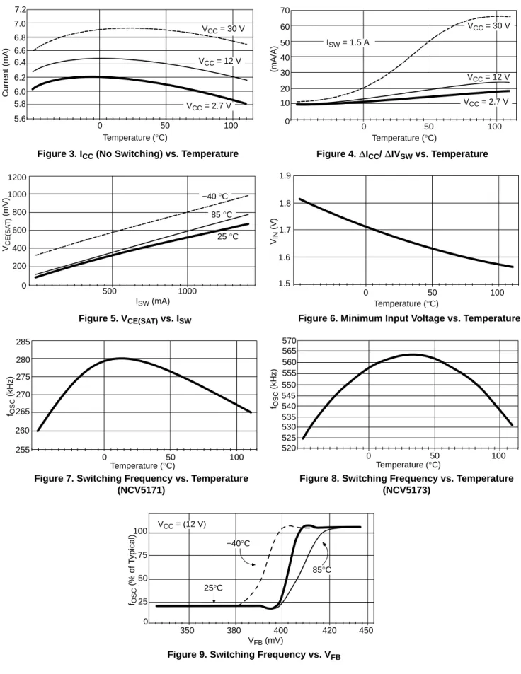
TYPICAL PERFORMANCE CHARACTERISTICS
0
Temperature (°C)
Figure 3. ICC (No Switching) vs. Temperature
Current (mA)
7.2 7.0 6.8 6.6 6.4 6.2 6.0 5.8
VCC = 30 V
5.6 50 100
VCC = 12 V
VCC = 2.7 V
0
Temperature (°C)
Figure 4. DICC/ DIVSW vs. Temperature
(mA/A)
70 60 50 40 30 20 10
50 100
VCC = 30 V
VCC = 12 V VCC = 2.7 V ISW = 1.5 A
0
ISW (mA) Figure 5. VCE(SAT) vs. ISW VCE(SAT) (mV)
1200 1000 800 600 400 200
0 500 1000
−40 °C 85 °C
25 °C
Temperature (°C)
Figure 6. Minimum Input Voltage vs. Temperature VIN (V)
1.5 1.6 1.7 1.8 1.9
0 50 100
Temperature (°C)
Figure 7. Switching Frequency vs. Temperature (NCV5171)
fOSC (kHz)
255 260 265 270 275
0 50 100
280 285
0
VFB (mV) fOSC (% of Typical)
100 75 50 25
350 VCC = (12 V)
380 400 420 450
85°C 25°C
−40°C
Figure 8. Switching Frequency vs. Temperature (NCV5173)
Figure 9. Switching Frequency vs. VFB
Temperature (°C) fOSC (kHz)
540 545 550 555 560
0 50 100
565 570
535 530 525 520
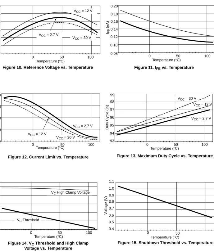
TYPICAL PERFORMANCE CHARACTERISTICS
Temperature (°C)
Voltage (V)
1.268 1.270 1.272 1.274 1.276
0 50 100
1.278 1.280
VCC = 12 V
VCC = 2.7 V
VCC = 30 V
Temperature (°C) IFB (mA)
0.08 0.10 0.12 0.14 0.16
0 50 100
0.18 0.20
Figure 10. Reference Voltage vs. Temperature Figure 11. IFB vs. Temperature
Temperature (°C)
Current (A)
2.20 2.30 2.40 2.50
0 50 100
2.60
VCC = 12 V
VCC = 30 V
VCC = 2.7 V
Temperature (°C) Duty Cycle (%)95
96 97 98
0 50 100
99
VCC = 30 V
VCC = 2.7 V
94 93
VCC = 12 V
Figure 12. Current Limit vs. Temperature Figure 13. Maximum Duty Cycle vs. Temperature
Temperature (°C)
Voltage (V)
0.5 0.6 0.7 0.8 0.9
0 50
1.0 1.1
0.4 Temperature (°C)
Voltage (V)
0.7 0.9 1.1 1.3
0 50 100
1.5 1.7
VC High Clamp Voltage
VC Threshold
Figure 14. VC Threshold and High Clamp Voltage vs. Temperature
Figure 15. Shutdown Threshold vs. Temperature
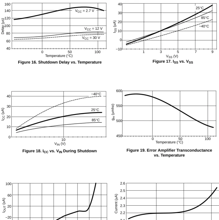
TYPICAL PERFORMANCE CHARACTERISTICS
Temperature (°C)
Delay (ms)
80 100 120 140
0 50 100
160
VCC = 12 V VCC = 30 V VCC = 2.7 V
60 40
VSS (V) ISS (mA)
10 20 30 40
1 5 7
−40°C
0
−10
85°C 25°C
3 9
Figure 16. Shutdown Delay vs. Temperature Figure 17. ISS vs. VSS
VIN (V) ICC (mA)
20 30 40
10
−40°C
10 0
85°C 25°C
Temperature (°C) gm (mmho)
450 500
0 50 100
550 600
Figure 18. ICC vs. VIN During Shutdown Figure 19. Error Amplifier Transconductance vs. Temperature
VREF −VFB (mV) IOUT (mA)
20 60 100
0
−20
−60 −255 −175 −125 −75 −25 25
Temperature (°C)
Current (mA)
2.6
0 50 100
2.5 2.4 2.3 2.2 2.1 2.0
Figure 20. Error Amplifier IOUT vs. VFB Figure 21. Switch Leakage vs. Temperature
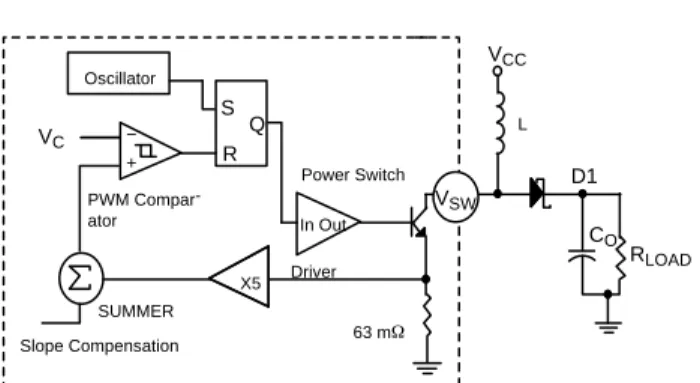
アプリケーション情報 動作原理電流モード制御
+
−
Driver
CO RLOAD VSW
X5 SUMMER Slope Compensation
VC Oscillator
D1 VCC
S R
Q
In Out PWM Compar-
ator
L
63 mW
Figure 22. Current Mode Control Scheme
Power Switch
NCV5171/73
昇$電源電流m
PWM -+nh生成電流67A御
方式採用(J!)-+nho-8+p#4比較(電源 q時間A御 ()発振rs定C波数.t.4(Ju用(
v定&'C波数[証()結果実現w A御方式R従来電$67A御Rx!
yzm{点*|})第 1 R-+nh T.m直接生成(-電$jR~座R
応答()R?bJ電$67KMt-v般的R見p#,Va>?@o- 8+R起遅延*1y1}) 2
番目X. 電流純R.-+
4La 4電流A限m得特有 {点最後R電流67電$1y p#電流A御,Va,V7 .a+Rv極E提()結
果比較能1電$67D路?}補 *容易R1}帯幅*高y1})
明確1OM*損1G4|}
)H5*電流67A御自Rs有題
R:Ve.a* 50% D状況c
調波発振*存()NCV5171/73 t+補 方式採用(発振r発生s定-+電
流-+R4題解決() 電流67A御{点犠牲R(1!D路安 定性改=BR適1 t+M*実現()
発振器とシャットダウン
VSW Current
Ramp Sync
発振r
18% C波数精度[証?R調整 wJ!) Figure 22 R示4>}、発振rp#、
280 kHz (NCV5171) )= 560 kHz (NCV5173) C波
数LZ qR()PWM KL p#R?bJLZ q,R1 })
SS X TTL Y換S期"#|} 発振r C波数最g 1.8 C波数S期4*I)
Figure 23 R示4>}?}高!C波数S期
=BR発振rp#*R1R正遷移 u用(JLZ qR(結果発
振r*OMw)S期&'R?}複数 電源*SvC波数&'I?R1})。
SS Xt.taR維持4 *P;MTUw電源電流*減少(
)
追機能RFB X* PQa7MO
4IRC波数称C波数 20% RP,M 412*|})電源投"過負荷)=短絡
状態4I最小 q時間PWM KL 最小La 幅R?bJA限w)
q,時間R?bJ最小:V e.a*減少(]^_部4 自[
護()
)=記4>}t. t+補 =B-+生成(安定性 改()
エラー・アンプ
+
− NCV5171/73
Figure 24. Error Amplifier Equivalent Circuit
1MW
positive error−amp 1.276 V
FB
VC C1
R1 5 kW 0.01 mF Voltage
Clamp 120 pF
FB X正o-8+0転"#R直接接
続wJ>}k非0転"#R1.276 V O,
電$*w) Figure 24 R示4>}、
8+約 1 M
W高p#XT 持zM- KT. 8+ V
CX o-8+p#R接続wJ>}部
0.5 1.7 V 範%.-+w) V
CX標
準的1接続4(J抵抗4Ke-7R 直 接続(a+補 =B極
/ ¡t形成 4*|})
]^_P;M V
CX4-7間R接続(
J.-+電$¢£4*I)結果的
スイッチ・ドライバとパワー・スイッチ
7-t.部mA御nh
¥_¦}p#LZ 駆&() o§抵抗 ( F計 63 m
W) ¨(J PGND X R接©wJ!) ª«*8
¬t-7m絶縁I?R PGND IC
板R接続wJ!)H5X.
電流部D路R?bJ.-+w).-
+電流 1.5 A D4*[証wJ>} t
+補 *®:Ve.a44R j ( ) L Z
最g
耐$ (V
SWXR接続wJ! ) K.i所 40 V 飽¯電$標準 1 V
未満|}消費電#最小wJ!)
短絡状態昇$D路短絡状態*生°4T.電流
* e.a期間±²("#
電源m過³1電流*引Ipw)A御
R負荷電流A限手段*1!=B ]部電流A限D路 ( d«´O12 ) 実装(J
負荷電源>?@ [護必要*|})kl構成 R蔵w=C
波数P,M機能R?}+>?@]^_部 損µ防止I)機能R?bJ最小:Ve.a*小wy1} *¶度q R1RM- 2
次·*過³1o¸a¹ºI)
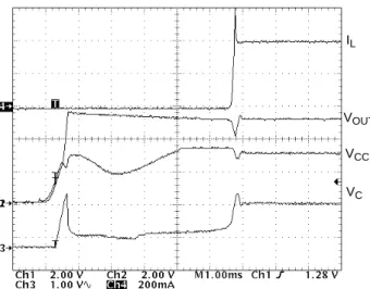
Figure 25. Startup Waveforms of Circuit Shown in the Application Diagram. Load = 400 mA.
IL
VOUT
VC VCC
V
CCX電$源R接続m SS X¸
aR4、 NCV5171/73 起&I) Figure 25 R示起&波形 PM 2 »
R| Application Diagram R示昇$K測
定(=波形"#電$*qR1b
=後R記録w=電源投"遷移¼種½
相示(J!)電$V
CC*最小電源電$¢D 4 V
SWXXT R1})
=B電流直接T.4Tq7
通°J"#電源mp#R流)*約
R達4部LZ *短時間¾_q
R1}) NCV5171/73 通常&'v部
部電流振幅*生°J!LZ *qR1b=4説明I)
V
CX電$* PQa7D4部L Z *}替G}始B V
SWX電$
La *生°) FB Xc!p#電$検p 4蔵C波数P,M機能* C
波数称¤¿1 mR¢£最小:V e.a*小wy1})kÀ]iF最小 :Ve.a 最小q時間R
?bJA限w),Á«X.電流 部電流A限R?bJ.-+w)
FB X電$* 0.4 V D4C波数称¤
)高y1}p#*安定電$R近ÂyRzJ X.電流*減少(始B)p#電$qP M8.:V1 (
電流)
引Ip(R?bJD避wk手法R?}過電$状態*検pw=iF 4o-8+P.電流*²()
過電$状態Fb X電$*O, 電$
50 mV ÀDiF4(J定義wJ!)
部品の選択 周波数補償
C波数補 目的P :Ã安定性[証(
1*望)(!過渡応答>?@ DC
安定達成4 Figure 26 R示4>}標準的1補 D
路
2 z極4 1 z¡t持zC波数応答実現(
)wRC波数応答 Figure 27 R示Ä 7線ÅÅ示()
NCV5171/73
Figure 26. A Typical Compensation Network VC
GND
C1 R1
C2
Figure 27 R示高! DC ->?@負
荷*j&状況
DC
精度達成=BR望)特性M- KT. o-8 + DC 次式計算4*I)
GainDC+GM ROG
M= o-8+M- KT.
R
O= o-8+p#抵抗≈ 1 M W
c!C波数極 f
P1À¢?Ro-8 +p#抵抗4 C1 求B4*I)
fP1+ 12pC1RO
C1 >?@ R1 ?bJ形成w第v¡tÀ¢4
>}
fZ1+ 1 2pC1R1
¡tR?bJ½相*進Ea+*.t q C波数少1y4 45
°½相f持z4*[証w)(=*bJ¡tÀ¢
C波数特定I電#段形成w極近 yR配置必要*|})
fP+ 1 2pCORLOAD
C
O= o-8+等Æp#9;LP
≈
120 pF;
R
LOAD=
負荷抵抗高!C波数極
f
P2p#,Va ESR *¡
tR1½置)= C波数 1/2 | C波数½置R配置I)C波数R極
配置4 ª«*減少()。極C波数
C2 >?@ R1 ¤R?bJ決)})
fP2+ 12pC2R1
適1½相f[証簡1方法
1 z
* 1 R1 ( v ) .t q点) C波数* 10 R14R −20 dB Ç斜持z C波数応答設計4.t qC波
数½相f*最gR1f
Z14 f
P2¼間点R 1?R選択必要*|})
Figure 27. Bode Plot of the Compensation Network Shown in Figure 26
Frequency (LOG) fP1
Gain (dB) DC Gain
fZ1
fP2
VSW電圧制限
昇$MÈt
V
SWX最g電$最g p#電$4p#Tq7
順方/電$¯R?bJ設定w)Tq7標準的1順方/電$
PQM9Tq7 0.5 V 超高速OÉ
OTq7 0.8 V
,-.MÈtX. V
SW電$次式決)})
VSW(MAX)+VCC(MAX))(VOUT)VF) N
N
=M- 巻数比1
次巻線/2
次巻線LZ *q,R1b=時点定常状
態電$R電$ L.*GbJ!)通常電$ L. V
SW4 PGND X間浮遊容量 Ê電M- O.T. R?b J発生() V
SWX電$*最g定格超1
!?RTq7R対(J直 過渡電$e+
ev次巻線RË R接続() 電
$.-+Ì方法過渡電$e+e V
SWX4-7間R接続4
磁気部品の選択磁気部選択4IX.電流K8>
?@,Á-M材質p#電$O+a EMI
温度範%物理的1gIw>?@Æ格12子考慮必要*|})昇$D路 100% o
¸aÍ送率Î定4平ÏT.電
流p#電流4電$(V
OUT/V
CC) 積表w )連続導通67T.O+a
電流次式決)})IRIPPLE+VCC(VOUT*VCC) (f)(L)(VOUT)
f = 280 kHz (NCV5171) )= 560 kHz (NCV5173) X.T.電流平Ï電流RO+
a電流Ð=電流*®
T.飽¯*生°1!?R必要*|}
))=式D路O+a電流許容
差RÂ!JT.¤選択4IRÑ 照4I)O+a電流*小w!iF"#Ke*小wy1}電流p#能#*
gIy14!{点*|})棒)=樽RÒ
=形状K8高!磁界放射Ç/*|})
*比較的安Æ小\MtTa12k l形状K8磁気a+*閉°J!=B
EMI 防止I)
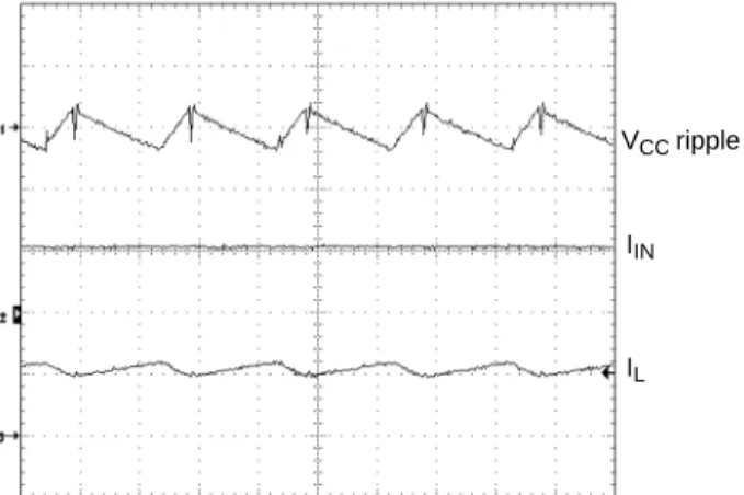
入力コンデンサの選択
Figure 29 R示4>}昇$D路T.*
"#,Vav部R1}) Figure 28 R示4>
}連続67"#電流波形Ó角形 gIyLa w=電流W)J!)H5 R?bJ"#Ke選択R課w条 Ô*減})連続導通67X. X.
T.O+a電流.PQ説明
()(= Figure 28 mGm4>}T.
VCC ripple
Figure 28. Boost Input Voltage and Current Ripple Waveforms
IIN
IL
+
−
Figure 29. Boost Circuit Effective Input Filter
VCC CIN
RESR
IL IIN
,-.D路状況*異1})"#電
流×連続gI1La 電流*"#KeR流)(=*bJ,-.
o¸a[存>?@,VaO 4! 2 z条Ô*KeR求B) +R対(J安定(=電源電$維持R 20
mF Dc ESR Ê電用Ke*必要 T.R?bJ生°ª«c減R V
CC4-7間+I¾_近y R 1.0
mF -§.Ke挿"()
VOUT ripple
IL
Figure 30 R示波形調Ø4p#電流O+a
* 2 z1N z)}Ke ESR 4p#
KeÊ放電m生°4*m})
昇$D路LZ *q,R14I
L* p#KeR流瞬間的1D V = I
IN ×ESR *
発生()S時R電流I
L− I
OUT*KeÊ
電(p#電$徐ÙR昇wH)LZ*qR14 I
l*-7RP;Mw I
OUTR?}p#Ke*放電w) I
LO+a*Ö小w!iF I
Lv定¤4(J扱
4*I"#電流 I
INR等(y1})
要約4p#電$X. X.O+a
À¢?R計算I)
VOUT(RIPPLE)+(IIN*IOUT)(1*D) (COUT)(f) ) IOUTD
(COUT)(f))IIN ESR
À¢?R式 V
CCV
OUT>?@ I
OUTu
用(J設計RÚ{1方法表現I)VOUT(RIPPLE)+IOUT(VOUT*VCC) (COUT)(f)
1 (COUT)(f) )(IOUT)(VOUT)(ESR)
VCC
Ke RMS O+a電流次式決)}
)
IRIPPLE+
Ǹ
(IIN*IOUT)2(1*D))(IOUT)2(D)+IOUT VOUT*VCC
Ǹ
VCC式昇$D路RE
適用I)*,-.D路Rz!JS様式導y4*I)
電流制限の低減
v部8+OÕPQ設計者*
電流A限¤4(J 1.5 A ¢D¤希望 4*|})]^_P;M V
CX4-7
間R接続(J.-+電$c減4*I)結果的R部LZM- 電流電
流A限*k称¤mc減w)V
CX電$次式評ÆI)
VC+ISWREAVR
E= 0.063 W部o§抵抗¤
A
V= 5 V/V 電流 8+
R
E>?@ A
Vo7ÛÜ (
設計者) *j更I 1! 電流 1.5 A
未満RA限=BRu用IÝv方法?}c!電$ V
CX .-+4最g 電流)=
最gT.電流式RÞ"4望)(
!.-+電$*得)
Figure 31 R示4>}簡1Tq7.- +u用(J V
C電$抵抗R3 電$RTq 7電$降¢=¤R.-+4*
I)残念1* V
IN安定精度*×Ö1 iFv般的R?1簡1D路u用I) H5
Figure 31. Current Limiting using a Diode Clamp VC
D1
VCC
R1 VIN
C2 C1 R2
R3
電流A限題R対Ì解決策 抵 抗u用(J 流電流]部測定
4k?1D路 Figure 32 R示()
− +
Figure 32. Current Limiting using a Current Sense Resistor
VC
RSENSE Q1
VCC
R1 VIN
C2 C1 R2
C3
Output Ground
PGND AGND
電流次¤RA限w)
ISWITCH(PEAK)+VBE(Q1)RSENSE
V
BE(Q1)= Q1 o§電$降¢ 0
標準
.65 V
改w=D路正常R&'wH安 定電$×要D路±的1率観点
{Ú性/()*残念1*Þ
必要設計者"#-74p#-7*ß通 1!4R注意必要*|}))=電流
抵抗 R
SENSE追4m1}gI
1電#損à*生°kRábJ:Ve
.a²()抵抗 R2 4Ke C3 *tL
,Va形成(Jª«除â()
低調波発振
c調波発振 (SHM) 電流67A御P :Ã見
題:Ve.a* 50% 超i FR×安定R1}) SHM 連続T.電
流*流 E発生()×安定性KR4bJ有害 1y通常p#電$安定R影響ãä(
)H5 SHM R?bJKm放射 EM ª
«*²(v定状況¢T.*高C波
聴ª«放射能性*|})
SHM 容易R改I題T.電
流立å*} t+部æ t+補ç補完w:Ve.a×安定性
*次 e.aRÍG防止(
) NCV5171/73 q時間±R
対(J標準
180 mA/
mgIw t+補 * 追wJ!)v部Õ qÄ7 t+補 *
存(J!JSHM *題414*|})
題è簡1対é法 t+補 g Iy(J望)(y1!発振防ê4k
Õ Figure 33 R示]部D路追(J
u用 t+補 量gIy4*I )D路必要4w 2 3
点部E|}蔵補 D路Ræ追çw)
Figure 33. Technique for Increasing Slope Compensation
VC
R1
C2 C1
R2
R3 VSW
C3
VSW
破線長方形%)=部o-8+
帯幅A限通常補 D路抵抗 R2 >
?@ R3 V
SWXm電$ëD路形成() 通常&' V
SW方形波 RÒJ!)*
KMÈtR?bJ異1})昇$M Èt>?@,-.MÈtR>_ V
SW計算=B式.PQæ V
SW電$A限çR記載(J!) *q,4I V
SW 電$KeC3 *Ê電w V
CX電$
方Rj() *qR14 C3 * R3
経由放電wV
CX負 t+*生成w )負 t+R?bJ t+補
*実現w)
D路R?bJ追w t+補 量
次式?R1})DI
DT+VSW
ǒ
R2)R3R3Ǔ ǒ1*eR3C3fSW*(1*D)Ǔǒ
(1*fSWD)REAVǓ
DI/
DT =
追w t+補 量(A/s)
V
SW= M- *q,R14I ª7電$
(V)
f
SW= C波数標準 280 kHz (NCV5171) )= 560 kHz (NCV5173) D = :Ve.a
R
E= 0.063
W部o§抵抗¤A
V= 5 V/V 電流 8+
t+補 D路R対適1¤選択際 R設計者)ì{Ú性高!Ke
選択(次R R2 >?@ R3 ¤選択(追w t
+補 量 100 mA/
ms R4>íB()
k後必要R応°J R2 ²減能性*|
})当然直 接続 R2 4 R3 組EFGH V
SWm過³1電流引I込)1!?RÖ
RgIy必要*|}))=A御a+
安定性確実R改=BR追Kȸ
MR?}形成w時定数次式?R選択 必要*|})
R3C3t1*D fSW
最後R t+補 追Rá!:V
e.a安定4過渡応答間RM7q,
関î*|4説明¾_Ƥ*|})o-8+適1&'ï£]部D路 *®
t+補 ðy追32過渡応答
遅y1})ソフトスタート
]部D路追4 NCV5171/73
部,§ORN,M M機能追I)N,M MD路 V
CX*起&時R急速RR14 防止(T.電流*急1 t+²
4防止()
Figure 34 R示D路必要4w部
数*最小SS Xu用(JK¶起&
4IR!zN,M MD路*起&
I?R()
Figure 34. Soft Start VC
R1
C2 C1 D1 D2
VCC
C3 VIN
SS SS
抵抗
R1 4Ke C1 >?@ C2 *補 D路形成 ()q時R V
CX電$*昇(
始BPQM9Tq7
D2 通°JK e C3 Ê電( V
CX電$.-+(J V
C*標準 1.05 V V
CPQa7R達4
*開始w?R() (
温度j 詳細Rz!J-,Ñ照)
VC+VF(D2))VC3
(=*bJ C3 V
CX電$A限4 D路起&遅y() C3 容量*gIy1 RzJN,M M時間長y1})。
SS *tiFTq7 D1 通°J C3 *放
電w) P;MTU機能u用(1!iF D1 ÉN7 V
INR接続必
要*|})接合部温度の計算
NCV5171/73 安±&'[証=BR設計者
q+消費電#計算(ñ期w接F
部温度求B必要*|})接F部温度*180
°C
±
30
°C D4部熱[護D路R?bJ q,R1})=¾(k?1高温 0復&'4&'寿ò確実R縮)})
接F部温度計算×正確*簡1'業。
最óR電#損à定量必要*|})
NCV5171/73 RÀ¢ 3 z1電#損à源*|}
)
発振r´Oô8?1部A御
D路 *q,4I少量電#必
要4()D路R起標準&'電流I
Q*
5.5 mA |4*PMõ様.
PQmGm})&'電流対温度-,m 追T *得)-, IQ *"#電$ V
IN>?@温度RgIy左öw 4示(J!)(=*bJ次式?R1}
)
PBIAS+VINIQ
qÄ7 NPN M- |
=B 7-電流考慮R"必要*
|})A御D路電流RJ電流* V
INX m
引I p w )
駆&
電流 DI
CC/
DI
SW)= M- KT.
4(Jõ様R記載wJ!)述?R
設計者-,追T 見z_4*I)k情÷u用(J設計者次式
?R計算I)
PDRIVER+VINISW ICCDISW D
I
SW= 通過電流
D = :Ve.a)= q
時間ëFI
SW>?@ D K+R?bJ異1}
)
昇$K ISW(AVG)^IL(AVG) D 1Efficiency D^VOUT*VIN
VOUT
,-.K
ISW(AVG)^VOUTILOADVIN
1 Efficiency
1 D D^ VOUT
VOUT)NSNPVIN
飽¯電$ V
(CE)SATq+電#
損
à R関
要1源 4 ( J
最 後 V
(CE)SAT部 NPN M- * 駆&電流 R?}飽¯領駆&w4IK. o§
電$ V
(CE)SATR関¤æ 飽¯
電$ç4(Jõ様)=-,m得)
(=*bJ
PSAT^V(CE)SATISW D
最後Rq+F計電#損àÀ¢?R
1})
PD+PBIAS)PDRIVER)PSAT
熱ù配gIwÉPMR
qJA)=接F部 C%熱抵抗4(J掲載wJ!) q
JA表面近y空気温度>?@
q+消費電#*Gm4q+接 F部温度計算I)
TJ+TA)(PDqJA)
T
J= )= FET 接F部温度 (
°C) T
A= C%温度 (
°C)
P
D=
該当 消費電#(W)
qJA=
接F部úC%熱抵抗(
°C/W) NCV5171/73 q
JA= 165
°C/W
設計者
T
J計算4 NCV5171/73 *8+OÕ
PQu用能m2m4!題解決I ) T
J*絶対最g許容接F部温度| 150
°C
DiF NCV5171/73 k8+OÕPQR
適(J!)H5
T
J* 150
°C R近!iF設計者接F部温度¢£
実現能1方法考慮必要*|})Ì KMÈt選択(J 電流小 wy4考)+表面R沿b=
空気流²´4
T
A*¢*能性考
)
電流レイアウトのガイドライン
2?1 電源正(y&'w HD路8UM非常R重要高速
電流4M T.
組EFGH4題引I起能性|
電$過渡*生°)=B8UMR関 (JÀ¢7-R従必要*|})
ûü
昇$D路Tq7p#Ke>?@q+LZM- m
成a+gI1AC
電流*循環() 関î|M >?@O7長wI¾_短y(J>y必要*|}),- .D路 AC g電流a+*M- ý·R存() 1
次·a+"#KeM- >?@q+L ZM- m成} 2
次·M- 整流Tq7>?@p#K e*Ìa+形成()昇$D路i F4±yS°?R AC g電流WþØJ M >?@O7短y(J>y必要*
ÿü |})
小電流nh-7電源-7m離(Jy¾w!最結果得=BR v点接©法)=-7+構造u
用(Jy¾w!3ü
電$,V7.抵抗 I¾_近yR配置(J敏感1,V7.配線 短y(J>!Jy¾w!,V7.抵
抗小電流8¬t-7R接続(Jy¾w!
NCV5171/73 3.3 VIN
VC (1 ) FB (2) 0.1 mF
VCC (5)
AGND (6) PGND (7)
VSW (8)
200 pF
MBRS120T3
22 mF 22 mH
Figure 35.
Additional Application Diagram,
3.3 V Input, 5.0 V/ 400 mA Output Boost Converter 10 mFGND
5.0 k
3.6 k
GND 5.0 VO
1.3 k
+ + +
NCV5171/73
+12 V
VC (1 ) FB (2) VCC (5)
AGND (6) PGND (7)
VSW (8)
MBRS140T3
22 mF
47 mF
Figure 36. Additional Application Diagram, 2.7 to 13 V Input, +12 V/ 200 mA Output Flyback Converter 1.0 mF
GND
2.0 k
10.72 k
GND
1.28 k
47 mF
47 nF 4.7 nF
VCC −12 V
T1
1:2 P6KE−15A
1N4148
MBRS140T3
NCV5171/73 VC (1 )
FB (2) VCC (5)
AGND (6) PGND (7)
VSW (8) 2.2 mF
15 mH GND
300
GND 5.0 k
.01 mF 200 pF
VIN
−5.0 VOUT 1.1 k
22 mF Low ESR
NCV5171/73
+
+
VC (1 )
FB (2) VCC (5)
AGND (6) PGND (7)
VSW (8) 22 mF
Figure 38. Additional Application Diagram, 2.7 V to 28 V Input, 5.0 V Output SEPIC Converter GND
12.76 k
GND
5.0 k .01 mF 200 pF
VCC
22 mH
LowESR 22 mF
22 mH 22 mF 37.24 k
5.0 V
NCV5171/73
VC FB
AGND PGND VSW
Figure 39. Additional Application Diagram, 4.0 V Input, 100 V/ 10 mA Output Boost Converter with Output Voltage Multiplier
GND
GND .01 m
VCC
4.0 V
Test SS 1 2 3 4
8 7 6 5 C11
R1 R2
R3 C10
.1 m
C8 C9
C1 C2 C3
C4 C5 C6
C7 .1 m
.1 m .1 m .1 m
50 V
50 V 50 V 50 V
.1 m 50 V .1 m
50 V .1 m
50 V
D1 D1 D1 D1 D1 D1 D1
1N4148 1N4148 1N4148 1N4148 1N4148 1N4148 1N4148 99.755 k/0.1 W, 1%
1.245 k/0.1 W, 1%
2.0 k .1 m
10 m
100 VO
+
+
+
NCV5171/73
VC FB
VCC AGND PGND VSW
GND GND
0.01 mF 200 pF
22 mF 15 mH
22 mF
1.28 k 5.0 k
SS Test 1 2 3
4 5
6 7 8
+5.0 V SS
C6 C1 R1
R2 R3
10.72 k
C5 22 mF C3 D2 D3
L1
D1
−12 V
+12 V C4
0.1 mF
PACKAGE DIMENSIONS
SOIC−8 NB CASE 751−07
ISSUE AK
SEATING PLANE 1
4 5 8
N
J
X 45_ K
NOTES:
1. DIMENSIONING AND TOLERANCING PER ANSI Y14.5M, 1982.
2. CONTROLLING DIMENSION: MILLIMETER.
3. DIMENSION A AND B DO NOT INCLUDE MOLD PROTRUSION.
4. MAXIMUM MOLD PROTRUSION 0.15 (0.006) PER SIDE.
5. DIMENSION D DOES NOT INCLUDE DAMBAR PROTRUSION. ALLOWABLE DAMBAR PROTRUSION SHALL BE 0.127 (0.005) TOTAL IN EXCESS OF THE D DIMENSION AT MAXIMUM MATERIAL CONDITION.
6. 751−01 THRU 751−06 ARE OBSOLETE. NEW STANDARD IS 751−07.
A
B S
H D
C
0.10 (0.004)
DIM A
MIN MAX MIN MAX
INCHES 4.80 5.00 0.189 0.197 MILLIMETERS
B 3.80 4.00 0.150 0.157 C 1.35 1.75 0.053 0.069 D 0.33 0.51 0.013 0.020
G 1.27 BSC 0.050 BSC
H 0.10 0.25 0.004 0.010 J 0.19 0.25 0.007 0.010 K 0.40 1.27 0.016 0.050
M 0 8 0 8
N 0.25 0.50 0.010 0.020 S 5.80 6.20 0.228 0.244
−X−
−Y−
G
Y M
0.25 (0.010)M
−Z−
Y 0.25 (0.010)M Z S X S
M
_ _ _ _
1.52 0.060
7.0 0.275
0.6 0.024
1.270 0.050 4.0 0.155
ǒ
inchesmmǓ
SCALE 6:1
*For additional information on our Pb−Free strategy and soldering details, please download the ON Semiconductor Soldering and Mounting Techniques Reference Manual, SOLDERRM/D.
SOLDERING FOOTPRINT*
ON Semiconductor and the ON logo are registered trademarks of Semiconductor Components Industries, LLC (SCILLC) or its subsidiaries in the United States and/or other countries.
SCILLC owns the rights to a number of patents, trademarks, copyrights, trade secrets, and other intellectual property. A listing of SCILLC’s product/patent coverage may be accessed at www.onsemi.com/site/pdf/Patent−Marking.pdf. SCILLC reserves the right to make changes without further notice to any products herein. SCILLC makes no warranty, representation or guarantee regarding the suitability of its products for any particular purpose, nor does SCILLC assume any liability arising out of the application or use of any product or circuit, and specifically disclaims any and all liability, including without limitation special, consequential or incidental damages. “Typical” parameters which may be provided in SCILLC data sheets and/or specifications can and do vary in different applications and actual performance may vary over time. All operating parameters, including “Typicals” must be validated for each customer application by customer’s technical experts. SCILLC does not convey any license under its patent rights nor the rights of others. SCILLC products are not designed, intended, or authorized for use as components in systems intended for surgical implant into the body, or other applications intended to support or sustain life, or for any other application in which the failure of the SCILLC product could create a situation where personal injury or death may occur. Should Buyer purchase or use SCILLC products for any such unintended or unauthorized application, Buyer shall indemnify and hold SCILLC and its officers, employees, subsidiaries, affiliates, and distributors harmless against all claims, costs, damages, and expenses, and reasonable attorney fees arising out of, directly or indirectly, any claim of personal injury or death associated with such unintended or unauthorized use, even if such claim alleges that SCILLC was negligent regarding the design or manufacture of the part. SCILLC is an Equal Opportunity/Affirmative Action Employer. This literature is subject to all applicable copyright laws and is not for resale in any manner.
()
ON Semiconductor\]ON*^_Semiconductor Components Industries, LLC (SCILLC)`(ab*cde*fg\]h"Ni*gjklmno,#$SCILLCCp noq0rstuv(wxyz){i*|5}~r'#r ~("#$SCILLC*>?hCp*' I)T*uYIN
k"#$www.onsemi.com/site/pdf/Patent-Marking.pdf. SCILLCE(,FK*>?* U{!"#$SCILLCIEC*5,*>?*[
I)()jY"Nj*>?jI)*YN ¡C¢£5¤£5¥¦5E§¨'()IE ¡9©{,ª":
;$SCILLCBt«RLM¬4*o®5¯@AB°±²t³´V)SE{9!µ¶*49W¤*·¸´!¹#¬
4!"#$o®5¯@AB º»#¼)*/0@ABE°±²t³)j*½¾¿ÀÁjI)ÂÃÄLM´j願IÅ ("#$SCILLCb*Cprb*i*r*TIEAÆ9pÇ(":;$SCILLC>?ÈÉÊ*ËÌ5ÍÎ 5{#tOÏÊ*ÐÑÒ 5{(N°±²t³"NSCILLC>?*ÓÔ[´ÕÖ×*ØÙÚ!X´E°±²t³EÛÊ* 78(NÜÝLM)jY"NMY
'{()j!":;$j*´E78LMN9*,EIp¬LM)IEI°±²t³SCILLC>? Þß"N(NZ[N{SCILLC b*à?*ÜÝ"N>á6()¸âVN{ãäLMN{()9b*´E78:å"Næp¬*6ç(NÕÖ×Y¢£è¤£5#¼ )*uÏ駨·éj´]êëìíEÛ j* ¡jI)îï j願IIN("#$"NSCILLC{b*ðñòxñcde6çdeóôõ' ()IE§¨9EI9*{("#$SCILLCö3d÷×høDùúöã,#$*ûíLMYüq0rý*'{EV)j!IEþý´V )9ÿ販#{,ª":;$
PUBLICATION ORDERING INFORMATION
N. American Technical Support: 800−282−9855 Toll Free USA/Canada
LITERATURE FULFILLMENT:
Literature Distribution Center for ON Semiconductor
ON Semiconductor Website: www.onsemi.com