General Description
The MAX11044/MAX11045/MAX11046 16-bit and MAX11054/MAX11055/MAX11056 14-bit ADCs offer 4, 6, or 8 independent input channels. Featuring independent track and hold (T/H) and SAR circuitry, these parts pro- vide simultaneous sampling at 250ksps for each channel.
The MAX11044/MAX11045/MAX11046 and MAX11054/
MAX11055/MAX11056 accept a ±5V input. All inputs are overrange protected with internal ±20mA input clamps providing overrange protection with a simple external resistor. Other features include a 4MHz T/H input bandwidth, internal clock, and internal or external reference. A 20MHz, bidirectional, parallel interface provides the conversion results and accepts digital configuration inputs.
The MAX11044/MAX11045/MAX11046 and MAX11054/
MAX11055/MAX11056 operate with a 4.75V to 5.25V analog supply and a separate flexible 2.7V to 5.25V digital supply for interfacing with the host without a level shifter. The MAX11044/MAX11045/MAX11046 are available in a 56-pin TQFN and 64-pin TQFP pack- ages while the MAX11054/MAX11055/MAX11056 are available in TQFP only and operate over the extended -40°C to +85°C temperature range.
Applications
Automatic Test Equipment
Power-Factor Monitoring and Correction Power-Grid Protection
Multiphase Motor Control Vibration and Waveform Analysis
Features
o 16-Bit ADC (MAX11044/MAX11045/MAX11046) and 14-Bit ADC (MAX11054/MAX11055/MAX11056)
8-Channel ADC (MAX11046/MAX11056) 6-Channel ADC (MAX11045/MAX11055) 4-Channel ADC (MAX11044/MAX11054) o Single Analog and Digital Supply
o High-Impedance Inputs Up to 1G Ω o On-Chip T/H Circuit for Each Channel o Fast 3µs Conversion Time
o High Throughput: 250ksps for Each Channel o 16-Bit/14-Bit, High-Speed, Parallel Interface o Internal Clocked Conversions
o 10ns Aperture Delay
o 100ps Channel-to-Channel T/H Matching o Low Drift, Accurate 4.096V Internal Reference
Providing an Input Range of ±5V
o External Reference Range of 3.0V to 4.25V,
Allowing Full-Scale Input Ranges of ±4.0V to ±5.2V o 56-Pin (8mm x 8mm) TQFN and 64-Pin
(10mm x 10mm) TQFP Packages o Evaluation Kit Available
MAX11044/MAX11045/MAX11046/MAX11054/MAX11055/MAX11056
Simultaneous-Sampling ADCs
________________________________________________________________ Maxim Integrated Products 1
Ordering Information
For pricing, delivery, and ordering information, please contact Maxim Direct at 1-888-629-4642, or visit Maxim’s website at www.maxim-ic.com.
PART PIN-PACKAGE CHANNELS MAX11044ETN+ 56 TQFN-EP* 4
MAX11044ECB+ 64 TQFP-EP* 4
MAX11045ETN+ 56 TQFN-EP* 6
MAX11045ECB+ 64 TQFP-EP* 6
MAX11046ETN+ 56 TQFN-EP* 8
MAX11046ECB+ 64 TQFP-EP* 8
MAX11054ECB+ 64 TQFP-EP* 4 MAX11055ECB+ 64 TQFP-EP* 6 MAX11056ECB+ 64 TQFP-EP* 8 Note: All devices are specified over the -40°C to +85°C operating temperature range.
+Denotes a lead(Pb)-free/RoHS-compliant package.
*EP = Exposed pad.
Functional Diagram
CLAMP S/H 16-/14-BIT ADC
CLAMP S/H 16-/14-BIT ADC
REF BUF
CONFIGURATION REGISTERS
INTERFACE AND CONTROL
BANDGAP REFERENCE
8 x 16-/14-BIT REGISTERS BIDIRECTIONAL DRIVERS CH0
AVDD
AGNDS
AGND CH7†
DB15**
DB0/CR0 DB3/CR3 DB4
EOC SHDN CONVST CS RD WR
DGND DVDD
RDC RDC_SENSE*
**MAX11044/MAX11045/MAX11046 †MAX11046/MAX11056 REFIO
INT REF 10kΩ
EXT REF
*CONNECTED INTERNALLY TO RDC ON THE TQFN PARTS MAX11044/MAX11045/MAX11046/
MAX11054/MAX11055/MAX11056
Pin Configurations appear at end of data sheet.
MAX11044/MAX11045/MAX11046/MAX11054/MAX11055/MAX11056
ABSOLUTE MAXIMUM RATINGS
ELECTRICAL CHARACTERISTICS
(V
AVDD= +4.75V to +5.25V, V
DVDD= +2.70V to +5.25V, V
AGNDS= V
AGND= V
DGND= 0V, V
REFIO= internal reference, C
RDC= 4 x 33µF, C
REFIO= 0.1µF, C
AVDD= 4 x 0.1µF || 10µF, C
DVDD= 3 x 0.1µF || 10µF; all digital inputs at DVDD or DGND, unless otherwise noted, f
SAMPLE= 250ksps. T
A= -40°C to +85°C, unless otherwise noted. Typical values are at T
A= +25°C.)
Stresses beyond those listed under “Absolute Maximum Ratings” may cause permanent damage to the device. These are stress ratings only, and functional operation of the device at these or any other conditions beyond those indicated in the operational sections of the specifications is not implied. Exposure to absolute maximum rating conditions for extended periods may affect device reliability.
AVDD to AGND ...-0.3V to +6V DVDD to AGND and DGND ...-0.3V to +6V DGND to AGND...-0.3V to +0.3V AGNDS to AGND...-0.3V to +0.3V CH0–CH7 to AGND ...-7.5V to +7.5V REFIO, RDC to AGND ...-0.3V to the lower of
(V
AVDD+ 0.3V) and +6V
EOC, WR, RD, CS, CONVST to AGND...-0.3V to the lower of(V
DVDD+ 0.3V) and +6V DB0–DB15 to AGND ...-0.3V to the lower of (V
DVDD+ 0.3V) and +6V
Maximum Current into Any Pin Except AVDD, DVDD, AGND, DGND ...±50mA Continuous Power Dissipation
56-Pin TQFN (derate 47.6mW/°C above +70°C) ....3809.5mW 64-Pin TQFP (derate 43.5mW/°C above +70°C)...3478mW Operating Temperature Range ...-40°C to +85°C Junction Temperature ...+150°C Storage Temperature Range ...-65°C to +150°C Lead Temperature (soldering, 10s) ...+300°C Soldering Temperature (reflow) ...+260°C
PARAMETER SYMBOL CONDITIONS MIN TYP MAX UNITS
STATIC PERFORMANCE (Note 1)
MAX11044/MAX11045/MAX11046 16
Resolution N
MAX11054/MAX11055/MAX11056 14 Bits
MAX11044/MAX11045/MAX11046 > -2 ±0.4 < +2
Integral Nonlinearity INL
MAX11054/MAX11055/MAX11056 -0.8 ±0.13 +0.8 LSB
MAX11044/MAX11045/MAX11046 > -1 ±0.4 < +1.2 Differential Nonlinearity DNL
MAX11054/MAX11055/MAX11056 -0.6 ±0.15 +0.6 LSB
MAX11044/MAX11045/MAX11046 16
No Missing Codes
MAX11054/MAX11055/MAX11056 14 Bits
Offset Error
±0.001
±0.015 %FSR
Channel Offset Matching
±0.001±0.015 %FSR
Offset Temperature Coefficient ±0.8 µV/°C
Gain Error ±0.015 %FSR
Positive Full-Scale Error
±0.015%FSR
Negative Full-Scale Error
±0.015%FSR
Positive Full-Scale Error Matching
±0.01%FSR
Negative Full-Scale Error Matching
±0.01%FSR
Channel Gain-Error Matching Between all channels ±0.01 %FSR
Gain Temperature Coefficient ±0.5 ppm/°C
DYNAMIC PERFORMANCE
M AX 11044/M AX 11045/
MAX11046 91 92.3
Signal-to-Noise Ratio SNR f
IN= 10kHz,
full-scale input M AX 11054/M AX 11055/
MAX11056 84.5 85.2
dB
M AX 11044/M AX 11045/
MAX11046 90.5 92
Signal-to-Noise and Distortion
Ratio SINAD f
IN= 10kHz,
full-scale input M AX 11054/M AX 11055/
MAX11056 84.5 85.2
dB
MAX11044/MAX11045/MAX11046/MAX11054/MAX11055/MAX11056
ELECTRICAL CHARACTERISTICS (continued)
(V
AVDD= +4.75V to +5.25V, V
DVDD= +2.70V to +5.25V, V
AGNDS= V
AGND= V
DGND= 0V, V
REFIO= internal reference, C
RDC= 4 x 33µF, C
REFIO= 0.1µF, C
AVDD= 4 x 0.1µF || 10µF, C
DVDD= 3 x 0.1µF || 10µF; all digital inputs at DVDD or DGND, unless otherwise noted, f
SAMPLE= 250ksps. T
A= -40°C to +85°C, unless otherwise noted. Typical values are at T
A= +25°C.)
PARAMETER SYMBOL CONDITIONS MIN TYP MAX UNITS
M AX 11044/M AX 11045/
MAX11046 98 104
Spurious-Free Dynamic Range SFDR f
IN= 10kHz,
full-scale input M AX 11054/M AX 11055/
MAX11056 95 104
dB
M AX 11044/M AX 11045/
MAX11046 -105 -98
Total Harmonic Distortion THD f
IN= 10kHz,
full-scale input M AX 11054/M AX 11055/
MAX11056 -104 -95
dB
Channel-to-Channel Crosstalk f
IN= 60Hz, full scale and ground on
adjacent channel (Note 2) -126 -100 dB
ANALOG INPUTS (CH0–CH7)
Input Voltage Range (Note 3) ±1.22 x
V
REFIOV
Input Leakage Current -1 +1 µA
Input Capacitance 15 pF
Input-Clamp Protection Current Each input simultaneously -20 +20 mA
TRACK AND HOLD
Throughput Rate Per channel 1 250 ksps
Acquisition Time t
ACQ1 1000 µs
-3dB point 4
Full-Power Bandwidth
-0.1dB point > 0.2 MHz
Aperture Delay 10 ns
Aperture-Delay Matching 100 ps
Aperture Jitter 50 ps
RMSINTERNAL REFERENCE
REFIO Voltage V
REF4.08 4.096 4.112 V
REFIO Temperature Coefficient ±5 ppm/°C
EXTERNAL REFERENCE
Input Current -10 +10 µA
REF Voltage-Input Range V
REF3.00 4.25 V
REF Input Capacitance 15 pF
DIGITAL INPUTS (CR0–CR3, RD, WR, CS, CONVST)
Input Voltage High V
IHV
DVDD= 2.7V to 5.25V 2 V
Input Voltage Low V
ILV
DVDD= 2.7V to 5.25V 0.8 V
Input Capacitance C
IN10 pF
Input Current I
INV
IN= 0V or V
DVDD±10 µA
MAX11044/MAX11045/MAX11046/MAX11054/MAX11055/MAX11056
ELECTRICAL CHARACTERISTICS (continued)
(V
AVDD= +4.75V to +5.25V, V
DVDD= +2.70V to +5.25V, V
AGNDS= V
AGND= V
DGND= 0V, V
REFIO= internal reference, C
RDC= 4 x 33µF, C
REFIO= 0.1µF, C
AVDD= 4 x 0.1µF || 10µF, C
DVDD= 3 x 0.1µF || 10µF; all digital inputs at DVDD or DGND, unless otherwise noted, f
SAMPLE= 250ksps. T
A= -40°C to +85°C, unless otherwise noted. Typical values are at T
A= +25°C.)
PARAMETER SYMBOL CONDITIONS MIN TYP MAX UNITS
DIGITAL OUTPUTS (DB0–DB15, EOC)
Output Voltage High V
OHI
SOURCE= 1.2mA V
DVDD-
0.4 V
Output Voltage Low V
OLI
SINK= 1mA 0.25 0.4 V
Three-State Leakage Current DB0–DB15, V
RD≥V
IHor V
CS≥V
IH10 µA
Three-State Output Capacitance DB0–DB15, V
RD≥ V
IHor V
CS≥ V
IH15 pF
Analog Supply Voltage AVDD 4.75 5.25 V
Digital Supply Voltage DVDD 2.70 5.25 V
MAX11046/MAX11056, V
AVDD= 5V 48
MAX11045/MAX11055, V
AVDD= 5V 39
Analog Supply Current I
AVDDMAX11044/MAX11054, V
AVDD= 5V 30
mA
MAX11046/MAX11056, V
DVDD= 3.3V 7.0
MAX11045/MAX11055, V
DVDD= 3.3V 6.5
Digital Supply Current (Note 9) I
DVDDMAX11044/MAX11054, V
DVDD= 3.3V 5.5
mA
I
DVDD10
Shutdown Current
I
AVDD10 µA
MAX11044/MAX11045/
MAX11046
±1
Power-Supply Rejection PSR
VAVDD = 4.9V to 5.1V
(Note 5) MAX11054/MAX11055/
MAX11056
±0.25LSB
TIMING CHARACTERISTICS (Note 4)
CONVST Rise to EOC t
CONConversion time (Note 6) 3 µs
Acquisition Time t
ACQ1 1000 µs
CS Rise to CONVST Rise
t
QSample quiet time (Note 6) 500 ns
CONVST Rise to EOC Rise t
047 140 ns
EOC Fall to CONVST Fall
t
1CONVST mode B0 = 0 only (Note 7) 0 ns
CONVST Low Time t
2CONVST mode B0 = 1 only 20 ns
CS Fall to WR Fall
t
30 ns
WR Low Time
t
420 ns
CS Rise to WR Rise
t
50 ns
Input Data Setup Time t
610 ns
Input Data Hold Time t
71 ns
CS Fall to RD Fall
t
80 ns
RD Low Time
t
930 ns
MAX11044/MAX11045/MAX11046/MAX11054/MAX11055/MAX11056
ELECTRICAL CHARACTERISTICS (continued)
(V
AVDD= +4.75V to +5.25V, V
DVDD= +2.70V to +5.25V, V
AGNDS= V
AGND= V
DGND= 0V, V
REFIO= internal reference, C
RDC= 4 x 33µF, C
REFIO= 0.1µF, C
AVDD= 4 x 0.1µF || 10µF, C
DVDD= 3 x 0.1µF || 10µF; all digital inputs at DVDD or DGND, unless otherwise noted, f
SAMPLE= 250ksps. T
A= -40°C to +85°C, unless otherwise noted. Typical values are at T
A= +25°C.)
PARAMETER SYMBOL CONDITIONS MIN TYP MAX UNITS
RD Rise to CS Rise
t
100 ns
RD High Time
t
1110 ns
RD Fall to Data Valid
t
1235 ns
RD Rise to Data Hold Time
t
13(Note 7) 5 ns
Note 1: See the Definitions section at the end of the data sheet.
Note 2: Tested with alternating channels modulated at full scale and ground.
Note 3: See the Input Range and Protection section for more details.
Note 4: C
LOAD= 30pF on DB0–DB15 and EOC. Inputs (CH0–CH7) alternate between full scale and zero scale. f
CONV= 250ksps.
All data is read out.
Note 5: Defined as the change in positive full scale caused by a ±2% variation in the nominal supply voltage.
Note 6: It is recommended that RD, WR, and CS are kept high for the quiet time (t
Q) and conversion time (t
CON).
Note 7: Guaranteed by design.
INTEGRAL NONLINEARITY vs. CODE (MAX1104_)
MAX11044 toc01
OUTPUT CODE (DECIMAL)
INL (LSB) 573444915232768 4096016384 245768192
-0.8 -0.6 -0.4 -0.2 0 0.2 0.4 0.6 0.8 1.0
-1.0 0 65536
VAVDD = 5.0V VDVDD = 3.3V fSAMPLE = 250ksps TA = +25°C VRDC = 4.096V
DIFFERENTIAL NONLINEARITY vs. CODE (MAX1104_)
MAX11044 toc02
OUTPUT CODE (DECIMAL)
DNL (LSB) 573444915232768 4096016384 245768192
-0.800 -0.600 -0.400 -0.200 0 0.200 0.400 0.600 0.800 1.000
-1.000 0 65536
VAVDD = 5.0V VDVDD = 3.3V fSAMPLE = 250ksps TA = +25°C VRDC = 4.096V
INL AND DNL vs. ANALOG SUPPLY VOLTAGE (MAX1104_)
MAX11044 toc03
VAVDD (V)
INL AND DNL (LSB)
5.15 5.05 4.95 4.85 -0.6
-0.2 0.2 0.6 1.0
-1.0
4.75 5.25
VDVDD = 3.3V fSAMPLE = 250ksps TA = +25°C VRDC = 4.096V
MAX INL
MAX DNL
MIN DNL MIN INL
Typical Operating Characteristics
(V
AVDD= 5V, V
DVDD= 3.3V, T
A= +25°C, f
SAMPLE= 250ksps, internal reference, unless otherwise noted.)
MAX11044/MAX11045/MAX11046/MAX11054/MAX11055/MAX11056
Typical Operating Characteristics (continued)
(V
AVDD= 5V, V
DVDD= 3.3V, T
A= +25°C, f
SAMPLE= 250ksps, internal reference, unless otherwise noted.)
ANALOG SUPPLY CURRENT vs. SUPPLY VOLTAGE
MAX11044 toc05
VAVDD (V) IAVDD (mA)
5.15 5.05 4.95 4.85 25
30 35 40 45
20
4.75 5.25
TA = +25°C fSAMPLE = 250ksps MAX11046 CONVERTING
MAX11045 CONVERTING
MAX11044 CONVERTING MAX11046 STATIC
MAX11045 STATIC
MAX11044 STATIC
DIGITAL SUPPLY CURRENT vs. SUPPLY VOLTAGE
MAX11044 toc07
VDVDD (V) IDVDD (mA)
4.75 4.25 3.75 3.25 2
4 6 8 10 12
0
2.75 5.25
TA = +25°C fSAMPLE = 250ksps
MAX11046 CONVERTING
MAX11044/MAX11045/MAX11046 STATIC MAX11045 CONVERTING
MAX11044 CONVERTING INL AND DNL vs. TEMPERATURE
(MAX1104_)
MAX11044 toc04
TEMPERATURE (°C)
INL AND DNL (LSB)
60 35 10 -15 -1.0
-0.5 0 0.5 1.0 1.5
-1.5
-40 85
VAVDD = 5.0V VDVDD = 3.3V fSAMPLE = 250ksps VRDC = 4.096V
MAX DNL
MIN DNL MAX INL
MIN INL
ANALOG SUPPLY CURRENT vs. TEMPERATURE
MAX11044 toc06
TEMPERATURE (°C) IAVDD (mA)
60 35 10 -15 25
30 35 40 45
20
-40 85
VAVDD = 5.0V fSAMPLE = 250ksps MAX11046 CONVERTING
MAX11045 CONVERTING
MAX11044 CONVERTING MAX11046 STATIC
MAX11045 STATIC
MAX11044 STATIC
MAX11044/MAX11045/MAX11046/MAX11054/MAX11055/MAX11056
DIGITAL SUPPLY CURRENT vs. TEMPERATURE
MAX11044 toc08
TEMPERATURE (°C) IDVDD (mA)
60 35 10 -15 1.2
2.4 3.6 4.8 6.0 7.2
0
-40 85
VDVDD = 3.3V fSAMPLE = 250ksps CDBxx = 15pF
MAX11046 CONVERTING
MAX11044/MAX11045/MAX11046 STATIC MAX11045 CONVERTING
MAX11044 CONVERTING
ANALOG AND DIGITAL SHUTDOWN CURRENT vs. TEMPERATURE
MAX11044 toc09
TEMPERATURE (°C)
SHUTDOWN CURRENT (µA)
60 35 10 -15 1
2 3 4 5
0
-40 85
VAVDD = 5.0V VDVDD = 3.3V
IAVDD
IDVDD
ANALOG AND DIGITAL SHUTDOWN CURRENT vs. SUPPLY VOLTAGE
MAX11044 toc09a
VAVDD OR VDVDD (V)
SHUTDOWN CURRENT (µA)
4.75 4.25 3.75 3.25 1
2 3 4 5
0
2.75 5.25
TA = +25°C
IAVDD
IDVDD
INTERNAL REFERENCE VOLTAGE vs. TEMPERATURE
MAX1960 toc11
TEMPERATURE (°C) VREFIO (V)
60 35
-15 10
4.084 4.088 4.092 4.096 4.104 4.100 4.108 4.112
4.080
-40 85
UPPER TYPICAL LIMIT VAVDD = 5.0V
LOWER TYPICAL LIMIT
OFFSET ERROR AND OFFSET ERROR MATCHING vs. TEMPERATURE
MAX11044 toc13
TEMPERATURE (°C)
ERRORS (%FS)
60 35 10 -15 -0.006
-0.002 0.002 0.006 0.010
-0.010
-40 85
fSAMPLE = 250ksps VAVDD = 5.0V VREFIO = 4.096V OFFSET ERROR MATCHING
OFFSET ERROR INTERNAL REFERENCE VOLTAGES
vs. SUPPLY VOLTAGE
MAX1960 toc10
VAVDD (V) VREF (V)
5.15 5.05 4.85 4.95 4.09595
4.09600 4.09605 4.09610 4.09620 4.09615 4.09625 4.09630
4.09590
4.75 5.25
VRDC
TA = +25°C
VREFIO
OFFSET ERROR AND OFFSET ERROR MATCHING vs. SUPPLY VOLTAGE
MAX11044 toc12
VAVDD (V)
ERRORS (%FS)
5.15 5.05 4.95 4.85 -0.006
-0.002 0.002 0.006 0.010
-0.010
4.75 5.25
fSAMPLE = 250ksps TA = +25°C VRDC = 4.096V OFFSET ERROR MATCHING
OFFSET ERROR
Typical Operating Characteristics (continued)
(V
AVDD= 5V, V
DVDD= 3.3V, T
A= +25°C, f
SAMPLE= 250ksps, internal reference, unless otherwise noted.)
MAX11044/MAX11045/MAX11046/MAX11054/MAX11055/MAX11056
GAIN ERROR AND GAIN ERROR MATCHING vs. SUPPLY VOLTAGE
MAX11044 toc14
VAVDD (V)
ERRORS (%FS)
5.15 5.05 4.95 4.85 -0.006
-0.002 0.002 0.006 0.010
-0.010
4.75 5.25
fSAMPLE = 250ksps TA = +25°C VRDC = 4.096V GAIN ERROR
GAIN ERROR MATCHING
GAIN ERROR AND GAIN ERROR MATCHING vs. TEMPERATURE
MAX11044 toc15
TEMPERATURE (°C)
ERRORS (%FS)
60 35 10 -15 -0.006
-0.002 0.002 0.006 0.010
-0.010
-40 85
fSAMPLE = 250ksps VAVDD = 5.0V VREFIO = 4.096V
GAIN ERROR
GAIN ERROR MATCHING
FFT PLOT (MAX1104_)
MAX11044 toc16
FREQUENCY (kHz)
MAGNITUDE (dB)
100 75 50 25 -120
-100 -80 -60 -40 -20 0
-140
0 125
fIN = 10kHz fSAMPLE = 250ksps TA = +25°C VAVDD = 5.0V
Typical Operating Characteristics (continued)
(V
AVDD= 5V, V
DVDD= 3.3V, T
A= +25°C, f
SAMPLE= 250ksps, internal reference, unless otherwise noted.)
SIGNAL-TO-NOISE RATIO AND SIGNAL-TO-NOISE AND DISTORTION RATIO vs. TEMPERATURE (MAX1104_)
MAX11044 toc18
TEMPERATURE (°C)
SNR AND SINAD (dB)
60 35 10 -15 91
92 93 94 95
90
-40 85
fIN = 10kHz fSAMPLE = 250ksps TA = +25°C VAVDD = 5.0V VRDC = 4.096V
VIN = -0.025dB FROM FS SNR
SINAD
SNR AND SINAD vs. ANALOG SUPPLY VOLTAGE (MAX1104_)
MAX11044 toc20
VAVDD (V)
SNR AND SINAD (dB)
5.15 5.05 4.95 4.85 91.5
92.0 92.5 93.0
91.0
4.75 5.25
fIN = 10kHz fSAMPLE = 250ksps TA = +25°C VRDC = 4.096V VIN = -0.025dB FROM FS
SNR
SINAD TWO-TONE IMD PLOT (MAX1104_)
MAX11044 toc17
FREQUENCY (kHz)
MAGNITUDE (dB)
12.0 11.2 10.4 9.6 8.8 8.0
7.2 12.8
fIN1 = 9838Hz fIN2 = 10235Hz fSAMPLE = 250ksps TA = +25°C VAVDD = 5.0V VRDC = 4.096V VIN = -0.01dBFS
-120 -100 -80 -60 -40 -20 0
-140
TOTAL HARMONIC DISTORTION vs. TEMPERATURE (MAX1104_)
MAX11044 toc19
TEMPERATURE (°C)
THD (dB)
60 35 10 -15 -106.0
-105.5 -105.0 -104.5 -104.0 -103.5
-106.5
-40 85
fIN = 10kHz fSAMPLE = 250ksps TA = +25°C VAVDD = 5.0V VRDC = 4.096V VIN = -0.025dB FROM FS
MAX11044/MAX11045/MAX11046/MAX11054/MAX11055/MAX11056
THD vs. ANALOG SUPPLY VOLTAGE (MAX1104_)
MAX11044 toc21
VAVDD (V)
THD (dB)
5.15 5.05 4.95 4.85 -106
-105 -104 -103 -102
-107
4.75 5.25
fIN = 10kHz fSAMPLE = 250ksps TA = +25°C VRDC = 4.096V VIN = -0.025dB FROM FS
SIGNAL-TO-NOISE AND DISTORTION RATIO vs. FREQUENCY (MAX1104_)
MAX11044 toc22
FREQUENCY (kHz)
SINAD (dB)
10 1
84 86 88 90 92 94
82
0.1 100
fSAMPLE = 250ksps TA = +25°C VAVDD = 5.0V VRDC = 4.096V VIN = -0.025dB from FS
THD vs. INPUT FREQUENCY (MAX1104_)
MAX11044 toc23
FREQUENCY (kHz)
THD (dB)
10 1
-105 -100 -95 -90 -85
-110
0.1 100
fSAMPLE = 250ksps TA = +25°C VAVDD = 5.0V VRDC = 4.096V VIN = -0.025dB from FS
Typical Operating Characteristics (continued)
(V
AVDD= 5V, V
DVDD= 3.3V, T
A= +25°C, f
SAMPLE= 250ksps, internal reference, unless otherwise noted.)
OUTPUT NOISE HISTOGRAM WITH INPUT CONNECTED TO AGNDS (MAX1104_)
MAX11044 toc25
OUTPUT CODE (DECIMAL) NUMBER OF OCCURANCES 50,000
100,000 150,000 200,000
0 32765 32766 32767 32768 32769 32770 32771
VCH_ = 0V VAVDD = 5.0V VRDC = 4.096V fSAMPLE = 250ksps
CONVERSION TIME vs. TEMPERATURE
MAX11044 toc27
TEMPERATURE (°C)
CONVERSION TIME (µs)
60 35
-15 10
2.93 2.94 2.95 2.96 2.98 2.97 2.99 3.00
2.92
-40 85
VAVDD = 5.0V CROSSTALK vs. FREQUENCY
MAX11044 toc24
FREQUENCY (kHz)
CROSSTALK (dB)
10 1
-130 -120 -110 -100 -90
-140
0.1 100
fIN = 60Hz fSAMPLE = 250ksps TA = +25°C VAVDD = 5.0V VRDC = 4.096V VIN = -0.025dB FROM FS INACTIVE CHANNEL AT AGNDS
CONVERSION TIME vs. ANALOG SUPPLY VOLATAGE
MAX11044 toc26
VAVDD (V)
CONVERSION TIME (µs)
5.15 5.05 4.85 4.95 2.93
2.94 2.95 2.96 2.98 2.97 2.99 3.00
2.92
4.75 5.25
TA = +25°C
MAX11044/MAX11045/MAX11046/MAX11054/MAX11055/MAX11056
Pin Description
PIN MAX11044
(TQFN-EP)
MAX11045 (TQFN-EP)
MAX11046 (TQFN-EP)
NAME FUNCTION
1 1 1 DB13 16-Bit Parallel Data Bus Digital Output Bit 13
2 2 2 DB12 16-Bit Parallel Data Bus Digital Output Bit 12
3 3 3 DB11 16-Bit Parallel Data Bus Digital Output Bit 11
4 4 4 DB10 16-Bit Parallel Data Bus Digital Output Bit 10
5 5 5 DB9 16-Bit Parallel Data Bus Digital Output Bit 9
6 6 6 DB8 16-Bit Parallel Data Bus Digital Output Bit 8
7, 21, 50 7, 21, 50 7, 21, 50 DGND Digital Ground
8, 20, 51 8, 20, 51 8, 20, 51 DVDD Digital Supply. Bypass to DGND with a 0.1µF capacitor at each DVDD input.
9 9 9 DB7 16-Bit Parallel Data Bus Digital Output Bit 7
10 10 10 DB6 16-Bit Parallel Data Bus Digital Output Bit 6
11 11 11 DB5 16-Bit Parallel Data Bus Digital Output Bit 5
12 12 12 DB4 16-Bit Parallel Data Bus Digital Output Bit 4
13 13 13 DB3/CR3 16-Bit Parallel Data Bus Digital Output Bit 3/
Configuration Register Input Bit 3
14 14 14 DB2/CR2 16-Bit Parallel Data Bus Digital Output Bit 2/
Configuration Register Input Bit 2
15 15 15 DB1/CR1 16-Bit Parallel Data Bus Digital Output Bit 1/
Configuration Register Input Bit 1
16 16 16 DB0/CR0 16-Bit Parallel Data Bus Digital Output Bit 0/
Configuration Register Input Bit 0
17 17 17
EOCActive-Low End-of-Conversion Output. EOC goes low when conversion is completed. EOC goes high when a conversion is initiated.
18 18 18 CONVST
C onver t S tar t Inp ut. Ri si ng ed g e of C ON V S T end s sam p l e and star ts a conver si on on the cap tur ed sam p l e.
The AD C i s i n acq ui si ti on m od e w hen C ON V S T i s l ow and C ON V S T m od e = 0.
19 19 19 SHDN
Shutdown Input. If SHDN is held high, the entire device will enter and stay in a low-current state. Contents of the configuration register are not lost when in the shutdown mode.
22, 28, 35, 43, 49
22, 28, 35, 43, 49
22, 28, 35, 43,
49 RDC
Refer ence Buffer D ecoup l i ng . C onnect al l RD C outp uts tog ether . Byp ass to AG N D w i th at l east an 80µF total cap aci tance. S ee the Layout, Gr ound i ng , and Byp assi ng secti on.
23, 27, 33, 38, 44, 48
23, 27, 33, 38, 44, 48
23, 27, 33, 38,
44, 48 AGNDS Signal Ground. Connect all AGND and AGNDS inputs
together on PCB.
MAX11044/MAX11045/MAX11046/MAX11054/MAX11055/MAX11056
Pin Description (continued)
PIN MAX11044
(TQFN-EP)
MAX11045 (TQFN-EP)
MAX11046 (TQFN-EP)
NAME FUNCTION
24, 30, 41, 47 24, 30, 41, 47 24, 30, 41, 47 AVDD Analog Supply Input. Bypass AVDD to AGND with a 0.1µF capacitor at each AVDD input.
25, 31, 40, 46 25, 31, 40, 46 25, 31, 40, 46 AGND Analog Ground. Connect all AGND inputs together.
32 29 26 CH0 Channel 0 Analog Input
34 32 29 CH1 Channel 1 Analog Input
37 34 32 CH2 Channel 2 Analog Input
39 37 34 CH3 Channel 3 Analog Input
36 36 36 REFIO External Reference Input/Internal Reference Output.
Place a 0.1µF capacitor from REFIO to AGND.
— 39 37 CH4 Channel 4 Analog Input
— 42 39 CH5 Channel 5 Analog Input
— — 42 CH6 Channel 6 Analog Input
— — 45 CH7 Channel 7 Analog Input
52 52 52
WRActive-Low Write Input. Drive WR low to write to the ADC. Configuration registers are loaded on the rising edge of WR.
53 53 54
CSActive-Low Chip-Select Input. Drive CS low when
reading from or writing to the ADC.
54 54 54
RDActive-Low Read Input. Drive RD low to read from the ADC. Each rising edge of RD advances the channel output on the data bus.
55 55 55 DB15 16-Bit Parallel Data Bus Digital Output Bit 15
56 56 56 DB14 16-Bit Parallel Data Bus Digital Output Bit 14
26, 29, 42, 45 26, 45 — I.C. Internally Connected. Connect to AGND.
— — — EP
E xp osed P ad . Inter nal l y connected to AG N D . C onnect to a l ar g e g r ound p l ane to m axi m i ze ther m al p er for m ance.
N ot i ntend ed as an el ectr i cal connecti on p oi nt.
MAX11044/MAX11045/MAX11046/MAX11054/MAX11055/MAX11056
Pin Description (continued)
PIN MAX11044
(TQFP-EP)
MAX11045 (TQFP-EP)
MAX11046 (TQFP-EP)
NAME FUNCTION
1 1 1 DB14 16-Bit Parallel Data Bus Digital Output Bit 14
2 2 2 DB13 16-Bit Parallel Data Bus Digital Output Bit 13
3 3 3 DB12 16-Bit Parallel Data Bus Digital Output Bit 12
4 4 4 DB11 16-Bit Parallel Data Bus Digital Output Bit 11
5 5 5 DB10 16-Bit Parallel Data Bus Digital Output Bit 10
6 6 6 DB9 16-Bit Parallel Data Bus Digital Output Bit 9
7 7 7 DB8 16-Bit Parallel Data Bus Digital Output Bit 8
8, 22, 59 8, 22, 59 8, 22, 59 DGND Digital Ground
9, 21, 60 9, 21, 60 9, 21, 60 DVDD Digital Supply. Bypass to DGND with a 0.1µF capacitor at each DVDD input.
10 10 10 DB7 16-Bit Parallel Data Bus Digital Output Bit 7
11 11 11 DB6 16-Bit Parallel Data Bus Digital Output Bit 6
12 12 12 DB5 16-Bit Parallel Data Bus Digital Output Bit 5
13 13 13 DB4 16-Bit Parallel Data Bus Digital Output Bit 4
14 14 14 DB3/CR3 16-Bit Parallel Data Bus Digital Output Bit 3/
Configuration Register Input Bit 3
15 15 15 DB2/CR2 16-Bit Parallel Data Bus Digital Output Bit 2/
Configuration Register Input Bit 2
16 16 16 DB1/CR1 16-Bit Parallel Data Bus Digital Output Bit 1/
Configuration Register Input Bit 1
17 17 17 DB0/CR0 16-Bit Parallel Data Bus Digital Output Bit 0/
Configuration Register Input Bit 0
18 18 18
EOCActive-Low End-of-Conversion Output. EOC goes low when conversion is completed. EOC goes high when a conversion is initiated.
19 19 19 CONVST
C onver t S tar t Inp ut. Ri si ng ed g e of C ON V S T end s sam p l e and star ts a conver si on on the cap tur ed sam p l e.
The AD C i s i n acq ui si ti on m od e w hen C ON V S T i s l ow and C ON V S T m od e = 0.
20 20 20 SHDN
Shutdown Input. If SHDN is held high, the entire device will enter and stay in a low-current state. Contents of the configuration register are not lost when in the shutdown mode.
23, 28, 32, 38, 43, 49, 53, 58
23, 28, 32, 38, 43, 49, 53, 58
23, 28, 32, 38,
43, 49, 53, 58 AGNDS Signal Ground. Connect all AGND and AGNDS inputs together on PCB.
24, 29, 35, 46, 52, 57
24, 29, 35, 46, 52, 57
24, 29, 35, 46,
52, 57 AVDD Analog Supply Input. Bypass AVDD to AGND with a 0.1µF capacitor at each AVDD input.
25, 30, 36, 45, 51, 56
25, 30, 36, 45, 51, 56
25, 30, 36, 45,
51, 56 AGND Analog Ground. Connect all AGND inputs together.
MAX11044/MAX11045/MAX11046/MAX11054/MAX11055/MAX11056
Pin Description (continued)
PIN MAX11044
(TQFP-EP)
MAX11045 (TQFP-EP)
MAX11046 (TQFP-EP)
NAME FUNCTION
26, 55 26, 55 26, 55 RDC_SENSE Reference Buffer Sense Feedback. Connect to RDC plane.
27, 33, 40, 48, 54
27, 33, 40, 48, 54
27, 33, 40, 48,
54 RDC
Refer ence Buffer D ecoup l i ng . C onnect al l RD C outp uts tog ether . Byp ass to AG N D w i th at l east an 80µF total cap aci tance. S ee the Layout, Gr ound i ng , and Byp assi ng secti on.
37 34 31 CH0 Channel 0 Analog Input
39 37 34 CH1 Channel 1 Analog Input
42 39 37 CH2 Channel 2 Analog Input
44 42 39 CH3 Channel 3 Analog Input
41 41 41 REFIO External Reference Input/Internal Reference Output.
Place a 0.1µF capacitor from REFIO to AGND.
— 44 42 CH4 Channel 4 Analog Input
— 47 44 CH5 Channel 5 Analog Input
— — 47 CH6 Channel 6 Analog Input
— — 50 CH7 Channel 7 Analog Input
61 61 61
WRActive-Low Write Input. Drive WR low to write to the ADC. Configuration registers are loaded on the rising edge of WR.
62 62 62
CSActive-Low Chip-Select Input. Drive CS low when
reading from or writing to the ADC.
63 63 63
RDActive-Low Read Input. Drive RD low to read from the ADC. Each rising edge of RD advances the channel output on the data bus.
64 64 64 DB15 16-Bit Parallel Data Bus Digital Output Bit 15
31, 34, 47, 50 31, 50 — I.C. Internally Connected. Connect to AGND.
— — — EP
E xp osed P ad . Inter nal l y connected to AG N D . C onnect to a l ar g e g r ound p l ane to m axi m i ze ther m al p er for m ance.
N ot i ntend ed as an el ectr i cal connecti on p oi nt.
MAX11044/MAX11045/MAX11046/MAX11054/MAX11055/MAX11056
Pin Description (continued)
PIN MAX11054
(TQFP-EP)
MAX11055 (TQFP-EP)
MAX11056 (TQFP-EP)
NAME FUNCTION
1 1 1 DB12 14-Bit Parallel Data Bus Digital Output Bit 12
2 2 2 DB11 14-Bit Parallel Data Bus Digital Output Bit 11
3 3 3 DB10 14-Bit Parallel Data Bus Digital Output Bit 10
4 4 4 DB9 14-Bit Parallel Data Bus Digital Output Bit 9
5 5 5 DB8 14-Bit Parallel Data Bus Digital Output Bit 8
6 6 6 DB7 14-Bit Parallel Data Bus Digital Output Bit 7
7 7 7 DB6 14-Bit Parallel Data Bus Digital Output Bit 6
8, 22, 59 8, 22, 59 8, 22, 59 DGND Digital Ground
9, 21, 60 9, 21, 60 9, 21, 60 DVDD Digital Supply. Bypass to DGND with a 0.1µF capacitor at each DVDD input.
10 10 10 DB5 14-Bit Parallel Data Bus Digital Output Bit 5
11 11 11 DB4 14-Bit Parallel Data Bus Digital Output Bit 4
12 12 12 DB3 14-Bit Parallel Data Bus Digital Output Bit 3
13 13 13 DB2 14-Bit Parallel Data Bus Digital Output Bit 2
14 14 14 DB1/CR3 14-Bit Parallel Data Bus Digital Output Bit 1/
Configuration Register Input Bit 3
15 15 15 DB0/CR2 14-Bit Parallel Data Bus Digital Output Bit 0/
Configuration Register Input Bit 2
16 16 16 CR1 Configuration Register Input Bit 1
17 17 17 CR0 Configuration Register Input Bit 0
18 18 18
EOCActive-Low End-of-Conversion Output. EOC goes low when conversion is completed. EOC goes high when a conversion is initiated.
19 19 19 CONVST
C onver t S tar t Inp ut. Ri si ng ed g e of C ON V S T end s sam p l e and star ts a conver si on on the cap tur ed sam p l e.
The AD C i s i n acq ui si ti on m od e w hen C ON V S T i s l ow and C ON V S T m od e = 0.
22, 28, 35, 43, 49
22, 28, 35, 43, 49
22, 28, 35, 43,
49 SHDN
Shutdown Input. If SHDN is held high, the entire device will enter and stay in a low-current state. Contents of the configuration register are not lost when in the shutdown mode.
23, 28, 32, 38, 43, 49, 53, 58
23, 28, 32, 38, 43, 49, 53, 58
23, 28, 32, 38,
43, 49, 53, 58 AGNDS Signal Ground. Connect all AGND and AGNDS inputs together on PCB.
24, 29, 35, 46, 52, 57
24, 29, 35, 46, 52, 57
24, 29, 35, 46,
52, 57 AVDD Analog Supply Input. Bypass AVDD to AGND with a 0.1µF capacitor at each AVDD input.
25, 30, 36, 45, 51, 56
25, 30, 36, 45, 51, 56
25, 30, 36, 45,
51, 56 AGND Analog Ground. Connect all AGND inputs together.
26, 55 26, 55 26, 55 RDC_SENSE Refer ence Buffer S ense Feed b ack. C onnect to RD C p l ane.
MAX11044/MAX11045/MAX11046/MAX11054/MAX11055/MAX11056
Detailed Description
The MAX11044/MAX11045/MAX11046 and MAX11054/
MAX11055/MAX11056 are fast, low-power ADCs that combine 4, 6, or 8 independent ADC channels in a sin- gle IC. Each channel includes simultaneously sampling independent T/H circuitry that preserves relative phase information between inputs making the MAX11044/
MAX11045/MAX11046 and MAX11054/MAX11055/
MAX11056 ideal for motor control and power monitor- ing. The MAX11044/MAX11045/MAX11046 and MAX11054/MAX11055/MAX11056 are available with
±5V input ranges that feature ±20mA overrange, fault- tolerant inputs. The MAX11044/MAX11045/MAX11046
and MAX11054/MAX11055/MAX11056 operate with a single 4.75V to 5.25V supply. A separate 2.7V to 5.25V supply for digital circuitry makes the devices compatible with low-voltage processors.
The MAX11044/MAX11045/MAX11046 and MAX11054/
MAX11055/MAX11056 perform conversions for all chan- nels in parallel by activating independent ADCs. Results are available through a high-speed, 20MHz, parallel data bus after a conversion time of 3µs following the end of a sample. The data bus is bidirectional and allows for easy programming of the configuration register. The MAX11044/MAX11045/MAX11046 and MAX11054/
MAX11055/MAX11056 feature a reference buffer, which
Pin Description (continued)
PIN MAX11054
(TQFP-EP)
MAX11055 (TQFP-EP)
MAX11056 (TQFP-EP)
NAME FUNCTION
27, 33, 40, 48, 54
27, 33, 40, 48, 54
27, 33, 40, 48,
54 RDC
Refer ence Buffer D ecoup l i ng . C onnect al l RD C outp uts tog ether . Byp ass to AG N D w i th at l east an 80µF total cap aci tance. S ee the Layout, Gr ound i ng , and Byp assi ng secti on.
37 34 31 CH0 Channel 0 Analog Input
39 37 34 CH1 Channel 1 Analog Input
42 39 37 CH2 Channel 2 Analog Input
44 42 39 CH3 Channel 3 Analog Input
41 41 41 REFIO External Reference Input/Internal Reference Output.
Place a 0.1µF capacitor from REFIO to AGND.
— 44 42 CH4 Channel 4 Analog Input
— 47 44 CH5 Channel 5 Analog Input
— — 47 CH6 Channel 6 Analog Input
— — 50 CH7 Channel 7 Analog Input
61 61 61
WRActive-Low Write Input. Drive WR low to write to the ADC. Configuration registers are loaded on the rising edge of WR.
62 62 62
CSActive-Low Chip-Select Input. Drive CS low when
reading from or writing to the ADC.
63 63 63
RDActi ve- Low Read Inp ut. D r i ve RD l ow to r ead fr om the AD C . E ach r i si ng ed g e of RD ad vances the channel outp ut on the d ata b us.
64 64 64 DB13 14-Bit Parallel Data Bus Digital Output Bit 13
31, 34, 47, 50 31, 50 — I.C. Internally Connected. Connect to AGND.
— — — EP
E xp osed P ad . Inter nal l y connected to AG N D . C onnect to a l ar g e g r ound p l ane to m axi m i ze ther m al p er for m ance.
N ot i ntend ed as an el ectr i cal connecti on p oi nt.
MAX11044/MAX11045/MAX11046/MAX11054/MAX11055/MAX11056
is driven by an internal bandgap reference circuit (V RE- FIO = 4.096V). Drive REFIO with an external reference or bypass with 0.1µF capacitor to ground when using the internal reference.
Analog Inputs Track and Hold (T/H) To preserve phase information across all channels, each input includes a dedicated T/H circuitry. The input tracking circuitry provides a 4MHz small-signal band- width, enabling the device to digitize high-speed tran- sient events and measure periodic signals with bandwidths exceeding the ADC’s sampling rate by using undersampling techniques. Use anti-alias filtering to avoid high-frequency signals being aliased into the frequency band of interest.
Input Range and Protection The full-scale analog input voltage is a product of the ref- erence voltage. For the MAX11044/MAX11045/
MAX11046 and MAX11054/MAX11055/MAX11056, the full-scale input is bipolar in the range of:
When in external reference mode, drive V REFIO with a 3.0V to 4.25V source, resulting in an input range of
±3.662V to ±5.188V, respectively.
All analog inputs are fault-protected to up to ±20mA.
The MAX11044/MAX11045/MAX11046 and MAX11054/
MAX11055/MAX11056 include an input clamping circuit that activates when the input voltage at the analog input is above (V AVDD + 300mV) or below –(V AVDD + 300mV).
The clamp circuit remains high impedance while the input signal is within the range of ±V AVDD and draws lit- tle or almost no current. However, when the input signal exceeds ±V AVDD , the clamps begin to turn on and shunt current to/from the AVDD supply. Consequently, to obtain the highest accuracy, ensure that the input voltage does not exceed ±(V AVDD + 0.3V).
To make use of the input clamps (see Figure 1), con- nect a resistor (R S ) between the analog input and the voltage source to limit the voltage at the analog input so that the fault current into the MAX11044/MAX11045/
MAX11046 and MAX11054/MAX11055/MAX11056 does not exceed ±20mA. Note that the voltage at the analog input pin limits to approximately 7V during a fault condi- tion so the following equation can be used to calculate the value of R S :
± (
. ) V REFIO x 5
4 096
MAX11044/MAX11045/MAX11046/
MAX11054/MAX11055/MAX11056
CLAMP S/H 16-/14-BIT ADC
CLAMP S/H 16-/14-BIT ADC
REF BUF
CONFIGURATION REGISTERS
INTERFACE AND CONTROL
BANDGAP REFERENCE
8 x 16-/14-BIT REGISTERS BIDIRECTIONAL DRIVERS CH0
SOURCE
AVDD
AGNDS
*CONNECTED INTERNALLY ON THE TQFN PARTS TO RDC
**MAX11044/MAX11045/MAX11046 †MAX11046/MAX11056 AGND
CH7†
DB15**
DB0/CR0 DB3/CR3 DB4
EOC SHDN CONVST CS RD WR
DGND DVDD
RDC
RDC_SENSE*
REFIO
INT REF 10kΩ
EXT REF RS
INPUT SIGNAL
PIN VOLTAGE
Figure 1. Required Setup for Clamp Circuit
MAX11044/MAX11045/MAX11046/MAX11054/MAX11055/MAX11056
where V FAULT_MAX is the maximum voltage that the source produces during a fault condition.
Figures 2 and 3 illustrate the clamp circuit voltage-cur- rent characteristics for a source impedance R S = 1280 Ω . While the input voltage is within the ±(V AVDD + 300mV) range, no current flows in the input clamps.
Once the input voltage goes beyond this voltage range, the clamps turn on and limit the voltage at the input pin.
Applications Information
Digital Interface The bidirectional, parallel, digital interface, CR0–CR3, sets the 4-bit configuration register. This interface con- figures the following control signals: chip select (CS), read (RD), write (WR), end of conversion (EOC), and convert start (CONVST). Figures 6 and 7 and the Timing Characteristics in the Electrical Characteristics table show the operation of the interface.
DB0–DB15/DB13 output the 16-/14-bit conversion result.
All bits are high impedance when RD = 1 or CS = 1.
CR3 (Int/Ext Reference) CR3 selects the internal or external reference. The POR default = 0.
0 = internal reference, REFIO internally driven through a 10k Ω resistor, bypass with 0.1µF capacitor to AGND.
1 = external reference, drive REFIO with a high-quality reference.
CR2 (Output Data Format) CR2 selects the output data format. The POR default = 0.
0 = offset binary.
1 = two’s complement.
CR1 (Reserved) CR1 must be set to 0.
CR0 (CONVST Mode) CR0 selects the acquisition mode. The POR default = 0.
0 = CONVST controls the acquisition and conversion.
Drive CONVST low to start acquisition. The rising edge of CONVST begins the conversion.
1 = acquisition mode starts as soon as the previous conversion is complete. The rising edge of CONVST begins the conversion.
Programming the Configuration Register To program the configuration register, bring the CS and WR low and apply the required configuration data on CR3–CR0 of the bus and then raise WR once to save changes.
CAUTION: When the configuration register is not being programmed, the host driving CR3–CR0 must relinquish the bus when the conversion results of the ADC are being read!
R V V
S = FAULT MAX _ mA - 7 20
CR3 CR2 CR1 CR0
Int/Ext Reference
Output Data Format
Must be set to 0
CONVST Mode
Table 1. Configuration Register
MAX11044 fig02
SIGNAL VOLTAGE AT SOURCE AND PIN (V) ICLAMP (mA)
-10
-30 10 30
30
-30 10
-10 -20 20
0
-50 50
RS = 1280Ω VAVDD = 5V
AT CH_ INPUT
AT SOURCE
Figure 2. Input Clamp Characteristics
MAX11044 fig03
SIGNAL VOLTAGE AT SOURCE AND PIN (V) ICLAMP (mA)
-4
-6 -2 0 2 4 6
30
-30 10
-10 -20 20
0
-8 8
RS = 1280Ω VAVDD = 5V
AT CH_ INPUT AT SOURCE
Figure 3. Input Clamp Characteristics (Zoom In)
MAX11044/MAX11045/MAX11046/MAX11054/MAX11055/MAX11056
Starting a Conversion CONVST initiates conversions. The MAX11044/
MAX11045/MAX11046 and MAX11054/MAX11055/
MAX11056 provide two acquisition modes set through the configuration register. Allow a quiet time (t Q ) of 500ns prior to the start of conversion to avoid any noise interference during readout or write operations from corrupting a sample.
In default mode (CR0 = 0), drive CONVST low to place the MAX11044/MAX11045/MAX11046 and MAX11054/
MAX11055/MAX11056 into acquisition mode. All the input switches are closed and the internal T/H circuits track the respective input voltage. Keep the CONVST signal low for at least 1µs (t ACQ ) to enable proper set- tling of the sampled voltages. On the rising edge of CONVST, the switches are opened and the MAX11044/MAX11045/MAX11046 and MAX11054/
MAX11055/MAX11056 begin the conversion on all the samples in parallel. EOC remains high until the conver- sion is completed.
In the second mode (CR0 = 1), the MAX11044/
MAX11045/MAX11046 and MAX11054/MAX11055/
MAX11056 enter acquisition mode as soon as the previ- ous conversion is completed. CONVST rising edge initi- ates the next sample and conversion sequence.
CONVST needs to be low for at least 20ns to be valid.
Provide adequate time for acquisition and the requisite quiet time in both modes to achieve accurate sampling and maximum performance of the MAX11044/
MAX11045/MAX11046 and MAX11054/MAX11055/
MAX11056.
Reading Conversion Results The CS and RD are active-low, digital inputs that con- trol the readout through the 16-/14-bit, parallel, 20MHz data bus (D0–D15/D13). After EOC transitions low, read the conversion data by driving CS and RD low. Each low period of RD presents the next channel’s result.
When CS or RD are high, the data bus is high imped- ance. CS may be driven high between individual chan- nel readouts or left low during the entire 8-channel readout.
Reference Internal Reference The MAX11044/MAX11045/MAX11046 and MAX11054/
MAX11055/MAX11056 feature a precision, low-drift, internal bandgap reference. Bypass REFIO with a 0.1µF capacitor to AGND to reduce noise. The REFIO output voltage may be used as a reference for other circuits. The output impedance of REFIO is 10k Ω . Drive only high impedance circuits or buffer externally when using REFIO to drive external circuitry.
External Reference Set the configuration register to disable the internal ref- erence and drive REFIO with a high-quality external ref- erence. To avoid signal degradation, ensure that the integrated reference noise applied to REFIO is less than 10µV in the bandwidth of up to 50kHz.
Sn Sn + 1
t8
t12 t13
t9 t10
t11 RD
(USER SUPPLIED) CS (USER SUPPLIED)
DB0–DB15/DB13
Figure 5. Readout Timing Requirements
CONFIGURATIONREGISTER t6
t3 t4
t5
t7 WR
(USER SUPPLIED) CS (USER SUPPLIED)
CR0–CR3 (USER SUPPLIED)
Figure 4. Programming Configuration-Register Timing
Requirements
MAX11044/MAX11045/MAX11046/MAX11054/MAX11055/MAX11056
S0 S1 S6 S7
SAMPLE
tQ tACQ
t2 tCON
tO CONVST
EOC
RD
DB0–DB15/DB13 CS
Figure 7. Conversion Timing Diagram (CR0 = 1)
S0 S1 S6 S7
SAMPLE
tQ tACQ
tCON
tO
t1 CONVST
EOC
RD
DB0–DB15/DB13 CS
Figure 6. Conversion Timing Diagram (CR0 = 0)
MAX11044/MAX11045/MAX11046/MAX11054/MAX11055/MAX11056
Reference Buffer The MAX11044/MAX11045/MAX11046 and MAX11054/
MAX11055/MAX11056 have a built-in reference buffer to provide a low-impedance reference source to the SAR converters. This buffer is used in both internal and external reference mode. The reference buffer output feeds five RDC pins. The RDC pins should be all con- nected together on the PCB. The reference buffer is
externally compensated and requires at least 10µF on the RDC node. For best performance, provide a total of at least 80µF on the RDC outputs.
Transfer Functions Figures 8 and 9 show the transfer functions for all the formats and devices. Code transitions occur halfway between successive-integer LSB values.
-FS 7FFF
0001 0000
8000 8001 FFFE
INPUT VOLTAGE (LSB)
OUTPUT CODE (hex)
FFFF
0 FULL-SCALE
TRANSITION
+FS +32,766.5 x VLSB -32,767.5 x VLSB
-FS = -32,768 x VLSB 7FFE
+FS = 32,767 x VLSB
VLSB = (10/4.096) x (VREF/65,536)
+ 32,768 OUTPUT CODE =
VLSB VIN
Figure 8. Two’s Complement Transfer Function for 16-Bit Devices
-FS 1FFF
0001 0000
2000 2001 3FFE
INPUT VOLTAGE (LSB)
OUTPUT CODE (hex)
3FFF
0 FULL-SCALE
TRANSITION
+FS +8190.5 x VLSB -8191.5 x VLSB
-FS = -8192 x VLSB 1FFE
+FS = 8191 x VLSB
VLSB = (10/4.096) x (VREF/16,384)
OUTPUT CODE = VLSB
VIN + 8192
Figure 9. Offset-Binary Transfer Function for 16-Bit Devices
OUTPUT CODE (hex)
FULL-SCALE TRANSITION
-FS FFFF
8001 8000
0000 0001 7FFE
INPUT VOLTAGE (LSB) 7FFF
0 +FS
FFFE
OUTPUT CODE =
VLSB = (10/4.096) x (VREF/65,536)
-FS = -32,768 x VLSB +FS = 32,767 x VLSB
+32,766.5 x VLSB -32,767.5 x VLSB
VLSB VIN
Figure 8b. Two’s Complement Transfer Function for 14-Bit Devices
OUTPUT CODE (hex)
FULL-SCALE TRANSITION
-FS 3FFF
2001 2000
0000 0001 1FFE
INPUT VOLTAGE (LSB) 1FFF
0 +FS
+8190.5 x VLSB -8191.5 x VLSB
3FFE
VLSB = (10/4.096) x (VREF/16,384)
OUTPUT CODE = VLSB
VIN -FS = -8192 x VLSB +FS = 8191 x VLSB
Figure 9b. Offset-Binary Transfer Function for 14-Bit Devices
MAX11044/MAX11045/MAX11046/MAX11054/MAX11055/MAX11056
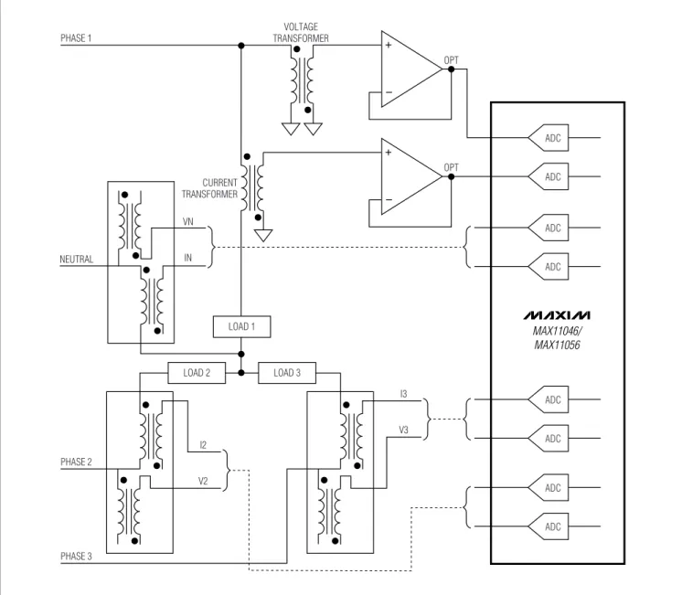
MAX11046/
MAX11056 ADC
ADC
ADC
ADC
ADC
ADC
ADC
ADC I3
V3 I2
V2 PHASE 2
PHASE 1
PHASE 3
LOAD 2 LOAD 1 VN
NEUTRAL IN
LOAD 3
OPT OPT
CURRENT TRANSFORMER
VOLTAGE TRANSFORMER
Figure 10. Power-Grid Protection
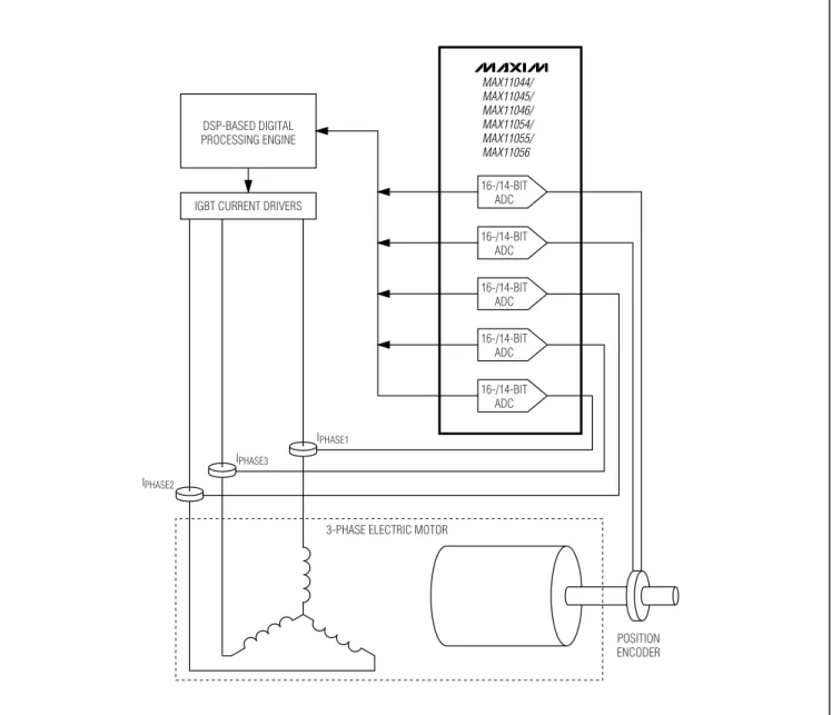
MAX11044/MAX11045/MAX11046/MAX11054/MAX11055/MAX11056
16-/14-BIT ADC MAX11044/
MAX11045/
MAX11046/
MAX11054/
MAX11055/
MAX11056
16-/14-BIT ADC
16-/14-BIT ADC
16-/14-BIT ADC
16-/14-BIT ADC
POSITION ENCODER DSP-BASED DIGITAL
PROCESSING ENGINE
IGBT CURRENT DRIVERS
IPHASE1
3-PHASE ELECTRIC MOTOR IPHASE3
IPHASE2