Shiro DOSHO†a),Member
SUMMARY This paper presents a tutorial overview of Continuous- Time Delta-Sigma Modulators (CTDSM); their operating principles to un- derstand what is important intuitively and architectures to achieve higher conversion efficiency and to operate low supply voltage, design methods against loop stability problem, tuning methods of the bandwidth and so on.
A survey of cutting-edge CMOS implementations is described.
key words: modulator, integrator, converter, stability, design method
1. Introduction
Delta-Sigma modulators are very popular architecture for digitizing the very small signals, which is widely used from voice to radio signals [1].
However, conventional modulators adopted switched capacitor architecture [2]–[4]. Thus the effective band- width of the modulator is not enough for a current wireless communication system required the bandwidth higher than 10 MHz.
On the other hand, the modulator with continuous-time integrators, which is called as “Continuous-Time Delta- Sigma Modulator”, has potential to operating at higher speed with lower conversion energy [5], [6]. It is the great advantage for the CTDSM to eliminate the anti-alias filter because the CTDSM acts as the role in its own. In addition, the modulator scatters smaller noise due to less switch archi- tecture, which is the very suitable characteristic for wireless communication systems [7].
Although continuous-time delta-sigma modula tors have many better characteristics as compared with discrete- time modulators, there are a number of practical issues and trade-offs for practical design [8]–[10].
It consumes much power to achieve high SNDR due to needs of higher order modulator. Lowering supply voltage for less power consumption causes larger harmonic distor- tions [11]–[13]. It needs large and complex filter to achieve multimode operation.
Moreover, the continuous-time modulator has difficul- ties about circuit design [14].
Especially, instability due to excess loop delay causes many design cycle re-runs, which is the most significant problem for circuit designer. In order to address these is- sues, significant efforts are focused to solve these issues for
Manuscript received November 26, 2011.
Manuscript revised January 23, 2012.
†The author is with Digital Core Development Center, Pana- sonic Corporation, Moriguchi-shi, 570-8501 Japan.
a) E-mail: [email protected] DOI: 10.1587/transele.E95.C.978
the last decade [15]–[17].
Therefore, in this paper, fundamental theory to under- stand characteristics of continuous-time delta-sigma modu- lator, various circuit techniques to realize the high efficient modulator operating under low supply voltage and design method taking into account of loop stability problem are presented.
Section 2 gives a brief fundamental theory of delta- sigma modulator, what is important to understand charac- teristics of the modulator intuitively is detailed. Section 3 surveys several circuit techniques; how to lowering the sup- ply voltage without increase of harmonic distortion, how to suppress power consumption, how to minimize circuit area and so on. Section 4 describes the tuning method of the modulator, which maximizes their performances. Section 5 details concrete design methods: conventional one to use classic filter theories and one to use more flexible optimiza- tion technique taking into account of loop stability. Sec- tion 6 sums up the state-of-the-art performance, trends, and challenges. The readers who are also interested in discrete time delta sigma modulators (DTDSMs) are recommended to see another tutorial paper [8].
2. Fundamentals of Delta-Sigma Modulators
2.1 Basic Characteristics
Figure 1 shows the basic concept of the delta-sigma modula- tor. The modulator is a kind of filter system for quantization noise by using a feedback loop.
The modulator is composed of the continuous-time RC-integrator, the quantizer and the feedback DAC. The in- tegrator amplifies the difference between analog input signal and the output of the DAC. The quantizer digitizes the out- put of the RC-integrator. The digital output codes of the quantizer are fed back to the input through the DAC.
The left side figure in Fig. 1(b) shows the ratio be- tween the input signal and quantization noise at the output in Fig. 1(a). At first, the input signal is multiplied by K(ω) which is the gain of the integrator. Then the quantizer adds the quantization noise to the amplified signal. The ratio of the quantization noise is very small because the signal is multiplied by very large gain of K(ω). Finally, feedback ef- fect suppresses the output signal so that the magnitude of the output is equal to the input signal. Thus, the magnitude of the quantization noise is suppressed to about 1/K(ω).
If K(ω) is integral function and the sampling rate is much Copyright c2012 The Institute of Electronics, Information and Communication Engineers
Fig. 1 Conceptual articulation of a delta-sigma modulator.
Fig. 2 Quantization noise spectrum of the modulator.
larger than the signal bandwidth, almost of the quantiza- tion noise is distributed at higher range of the signal band as shown in Fig. 2.
If the integrator in Fig. 1 is substituted with resonator, the shape of the quantization noise is flip vertical of the res- onator transfer function. Thus, the quantization noise de- creases at resonant frequency of the resonator as shown in Fig. 3.
This type of the modulator is called as a “Band-Pass delta-sigma modulator”, which is often used in wireless re- ceivers in order to convert IF signal to digital codes directly [18]–[22].
Another important point to understand characteristics of the modulator is that the modulator is a feedback sys- tem, which means that the feedback signal coincide with the input signal with accuracy of 1/K (K is the DC gain of the K(ω)). This is effective even if the feedback DAC has a large distortion.
Let’s confirm the effect by the simulation. Figure 4 shows the simulation result of the modulator with nonlinear DAC.
Even if the DAC in Fig. 4 has a large distortion, ana-
Fig. 3 Band-pass delta-sigma modulator.
Fig. 4 Simulation results of modulator with large distortion DAC.
log feedback signal (DAC output) has small distortion due to suppression by the large feed back gain. In contrast, the digital codes (Quantizer output) have the large distortion in compensation for better linearity of the analog feedback sig- nal. Therefore, the DAC linearity is one of the most impor- tant factors to achieve enough SNDR of the modulator.
Another imperfection of the DAC, which negatively af- fects the SNDR, is jitter of the DAC pulse. Figure 5 shows the comparison of settling behaviors between DT and CT integrator. Even if the sampling jitter exists, the output of the integrator settles the constant value ofVin∗C1/C2, which is not affected by the jitter. In contrast, the output of the CT-integrator fluctuates because input DAC pulse power also fluctuates due to sampling jitter. The variation of the pulse width (ΔTp) directly appears at the integrator output asΔTp∗Iin/C.
As just described DAC characteristics greatly affects the SNDR of the modulator. Using 1 bit DAC gives us
Fig. 5 Comparison settling behaviors with sampling jitter.
the perfect linearity. However, the affection of the jitter noise becomes the highest because the amplitude of one bit change is also the highest. In the usual case of the CTDSM, multi-bit DAC is used to lower the jitter power and dynamic element matching (DEM) method is used to suppress the DAC nonlinearity [23], [24].
An alternative to get high SNDR is using 1 bit Switched Capacitor DAC (SC-DAC) making sampling rate as high as possible, because SC-DAC greatly reduce the influence of the jitter [25]. However, it is difficult to realize CTDSM with high bandwidth suitable for wireless communication sys- tems by using the alternative because it needs much higher sampling rate as compared with one using multi-bit DAC with DEM.
2.2 Effect of Excess Loop Delay
In case of the discrete time delta-sigma modulator (DT- DSM as shown in Fig. 6(a)), no excess loop delay is caused as long as the quantizer latch process settles within the inte- grate period as shown in Fig. 6(b).
On the other hand, CTDSM has the excess loop delay that is caused by both the quantizer delay and the excess phase shift of the integrator as shown in Fig. 7. The excess delay degrades the loop stability. Even 2nd-order CTDSM might cause oscillation when the delay is large.
The circuit architecture to compensate the excess loop delay is described in Sect. 3.
2.3 Design of the Integral Path
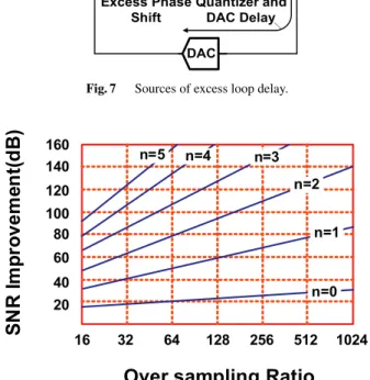
On the DSM, the ideal improvement of SNR from Nyqist- ADC is calculated as follows.
q2rms
e2rms = π2n
(2n+1)OS R2n+1 (1)
Here, qrms, erms, and n are in-band quantization noise of DSM, that of Nyquist-ADC and the order of the integra-
Fig. 6 Block and operation diagrams of DT-DSM.
Fig. 7 Sources of excess loop delay.
Fig. 8 Ideal SNR improvement of DSM against Nyquist-ADC.
tor, respectively. Figure 8 shows the improvement graphi- cally.
In order to achieve low power CTDSM with high band- width, it is inevitable to lower the oversampling rate. It is obvious that high order integrators greatly help for reducing oversampling rate with keeping high SNR.
However, high order integrators in DSMs have a loop stability problem, which cause DMSs to overflow. Taking into account of the stability problem, practical improve- ments of SNR are much less than the ideal case as shown
Fig. 9 Practical SNR improvement of DSM (without zeros) against Nyquist-ADC.
Fig. 10 Practical SNR improvement of DSM (with zeros) against Nyquist-ADC.
Fig. 11 Block diagram of CTDSM with NTF with Zero.
in Fig. 9, which empirically resulted from non-zero integral functions [26]. It is apparent from the figure that high order integrators are not effective until oversampling rate is over 32.
On the other hand, integrator with resonator is suitable when we have to use lower oversampling rate. The resonator introduce zero into the transfer function of the quantization noise, which enhance the SNR.
Figure 11 shows the block diagram of the CTDSM with NTF (Noise Transfer Function), whose transfer function has zero. Then Fig. 10 shows the practical improvement of SNR in this case, respectively.
Optimum positions for each order of integrant are sum- marized in the Table 1 [27]. As shown in Fig. 10, inserting zeros improves SNR especially at low oversampling rate.
Inverse Chebyshev filters are suitable for NTF proto- type because those filter have zeros in the stop band [28].
Note that the first stage should be an integrator, because it increases the input equivalent noise to place a resonator at the first stage. Thus odd order transfer function is suitable for this type circuit configuration.
The peak gain of the NTF which is called as “Out Band Gain(OBG)” is a quite significant factor because the OBG affects not only the loop stability but also the sensitivity of SNR to clock jitter [29].
Sampling jitter of the DAC causes pulse width errors, which is modulated by the code shift of the DAC. The am- plitude of the code shift is correlated with the OBG. Thus, the jitter sensitivity depends on the OBG.
3. Circuit Techniques
In this section, several circuit techniques essentially need to realize a high performance CTDSM are presented.
3.1 Low Distortion Architecture
Figure 12 compares the circuit configurations between con- ventional and low distortion CTDSM [30], [31]. In the con- ventional one as shown in Fig. 12(a), both input signal and quantization noise go through the same integration path. On the other hand, in the low distortion architecture, the input signal fed to both the integral path and input of the quantizer so that only quantization noise goes through different paths.
Thus, the nonlinearity of the integration path doesn’t affect the input signal. Additionally, using multi-bit quan- tizer can reduce the dynamic range of the integration path, because the magnitude of the quantization noise of multi-bit quantizer becomes 1/2n−1 of one bit case. The drawback of the architecture is that the input signal is not filtered by the integrator due to the bypass. It means that an additional anti-alias filter is needed for this architecture.
3.2 Compensation of the Excess Loop Delay
This section details how to compensate the excess loop de- lay caused by the quantizer and path to the DAC in the CTDSM. Figure 13 shows the block diagram of the CTDSM with transfer functions of each block.
Here, we define the signal transfer function (STF)
Fig. 12 Low distortion CTDSM.
Fig. 13 Block diagram of the CTDSM with multiple feedback.
Fig. 14 Block diagram of the CTDSM with multiple feed-forward.
and quantization noise transfer function (NTF) as following equations.
S T F =Sn(z)/Nd(z)
NT F=Nn(z)/Nd(z) (2)
Figure 13 is multiple feedback type configuration in which we can design any Sn(z) and NTF. On the other hand, a multiple feed-forward type configuration as shown in Fig. 14 determines the STF automatically once the NTF is defined.
The STF of Fig. 14 is expressed as following equation.
STF =Sn(z)
1−Nn(z) Nd(z)
(3) In order to compensate the excess loop delay, trans- fer function in the feedback path (Nd(Z)−Nn(Z)) has to be slightly changed so that we can extract the term ofz−1 from Nd(Z)−Nn(Z). That is, the feedback transfer func- tion should be modified by the coefficient ofα, as following process [32].
αNd(z−1)−Nn(z−1) = z−1Ndn(z−1) (4) The coefficientα is determined so that the Eq. (4) has no zero order term. The block diagram corresponding with Eq. (4) is shown in Fig. 15.
Figure 15 is furthermore transformed as following equation.
Ndn(z−1)
Nn(z−1) = β+Ndn(z)
Nn(z) (5)
Fig. 15 Extraction ofz−1from feedback path.
Fig. 16 Final diagram for compensation of excess loop delay.
Finally, the block diagram of the CTDSM is modified as shown in Fig. 16.
For example, we assume the NTF as following transfer function.
NTF(z)= z5−4.951z4+9.855z3−9.855z2+4.951z−1 z5−3.606z4+5.347z3−4.049z2+1.56z−0.244 (6) Then, we have to express NTF(z) with z−1, which is represented as follows.
NTF(z−1)= z−5−4.951z−4+9.855z−3−9.855z−2+4.951z−1−1 0.244z−5−1.56z−4+4.049z−3−5.347z−2+3.606z−1−1 (7) Here, Nd(z−1) and Nn(z−1) are automatically deter- mined.
Nd(z−1)=0.244z−5−1.56z−4+4.049z−3−5.347z−2+3.606z−1−1 (8) Nn(z−1)=z−5−4.951z−4+9.855z−3−9.855z−2+4.951z−1−1 (9) Therefore, Eq. (4) is calculated as following equation.
αNd(z−1)−Nn(z−1)
=z−1Ndn(z−1)
=z−1
−0.756z−4+3.391z−3−5.806z−2+4.508z−1−1.345 (10) Finally,Ndn(z−1)/Nn(z−1) can convert the final form as following.
Ndn(z−1)
Nn(z−1) =β+Ndn (z) Nn(z)
= −0.756z−4+3.391z−3−5.806z−2+4.508z−1−1.345
z−5−4.951z−4+9.855z−3−9.855z−2+4.951z−1−1
= 1.345z5−4.508z4+5.806z3−3.391z2+0.756z z5−4.951z4+9.855z3−9.855z2+4.951z−1
=1.345− 2.152z4−7.449z3+9.864z2−5.903z+1.345
z5−4.951z4+9.855z3−9.855z2+4.951z−1 (11)
Fig. 17 Second order integrator with single opamp.
Therefore,β=1.345 in this example.
3.3 High Order Integration with Single Opamp
Although, the excess loop delay caused in the quantizer and DAC is compensated by the direct feedback path as shown in Sect. 3.2, the effect of excess phase shift caused in the inte- grator still remains. High order integration with one opamp is effective way to suppress the phase shift.
So far, several circuits involved this topic have been reported [95], [96]. However, flexibility of NTF is limited as compared with the technique mentioned below.
Figure 17 shows the circuit schematic of a 2nd order in- tegrator with single opamp. The transfer function of Fig. 17 is following.
Vo
Vin =− sR3(C3+C2)+1
s2C3C2R3(sC1R2R1+R2+R1) (12) If the following conditions are satisfied, the transfer function becomes 2nd order integral as expressed follows.
If C1
R1R2
R1+R2 =(C2+C3)R3 then Vo
Vin
= 1
s2C1
C
2C3 C2+C3
R1R2
(13) The circuit shown in Fig. 17 also realizes 1st order inte- gral function. The transfer function from current input from I1toVois calculated as follows.
Vo
I1 =− 1 sC3
(14) The current input from I2 enables 2nd order integral function as follows.
Vo
I2 =− R1(sR3(C3+C2)+1)
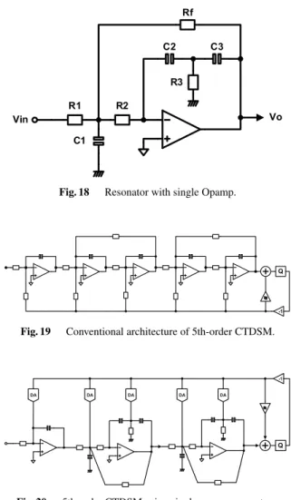
s2C3C2R3(sC1R2R1+R2+R1) (15) The integrator shown in Fig. 17 can be modified to res- onator by adding a feedback resistor between the output of the opamp and terminal ofV1as shown in Fig. 18.
The resonance condition of the resonator is following.
⎧⎪⎪⎪⎪⎨
⎪⎪⎪⎪⎩
C1=C2+C3
R3= 1 R11+1
R2+ 1 Rf
(16)
Fig. 18 Resonator with single Opamp.
Fig. 19 Conventional architecture of 5th-order CTDSM.
Fig. 20 5th-order CTDSM using single opamp resonators.
Assuming that these conditions are satisfied, the trans- fer function of Fig. 18 is calculated as follows.
Vo
Vin =− 1
C2C3R1R2
s2+ 1 C2C3R2Rf
(17)
Figure 19 shows the conventional architecture of 5th- order CTDSM that needs five opamps equal to order of in- tegration.
In contrast, only three opamps are needed for new ar- chitecture using the single opamp resonator as shown in Fig. 20. The new architecture gives us some benefits; re- duction of power consumption due to use of less number of opamp, reduction of GB products due to less excess phase shift through integration path, more stable operation of the resonator itself due to use of only one opamp.
Moreover, the function of the single Opamp resonator is expanded by making multi-path inputs as shown in Fig. 21 [33].
By adding input paths throughCin1 andCin2, the res- onator can realize the any 2nd order transfer function with a resonating pole. The transfer function of Fig. 21 is follow- ing.
Fig. 21 Schematic of single opamp resonator with multi-path inputs.
Fig. 22 5th-order CTDSM using multi-path single opamp resonator.
Vo
Vin =− Cin2
C3 s2+ Cin1
C2C3R2s+ 1 C2C3R1R2
s2+ 1 C2C3R2Rf
(18)
Equation (18) has high flexibility, because the each term in the numerator can be changed independently. Thus, Cin2changes the 2nd order term,Cin1changes the 1st order term andR1changes the zero order term, respectively. Rf
also determines the position of the pole independently.
Figure 22 shows another 5th-order CTDSM using multi-path Single opamp Resonator. In this case, only two feedback DACs are needed and the low distortion architec- ture as shown in Fig. 12(b) is applicable. Several derivative single opamp resonators are invented in order to enhance the FOM.
Finally, the concept of the single opamp resonator is extended to complex frequency region [34]–[38]. Figure 23 shows another circuit configuration of the complex res- onator based on the 2nd order integrator. The transfer func- tion of the Fig. 23 is expressed as following equation.
VoI+jVoQ
VI+jVQ
=− s−jC1
4R f3 s−jC1
2R f2
·CC43+ s−jC1
2R f2
·C31R4+C2C31R1R2
s−jC1
3R f1 s−jC1
2R f2
(19)
In this case, it is essential for cross coupled resistors (Rf1,Rf2,Rf3) to satisfy following conditions, in order to
Fig. 23 Complex resonator based on 2nd-order integrator.
cause all cross coupled resistors same frequency shift.
⎧⎪⎪⎪⎪⎪⎪⎨
⎪⎪⎪⎪⎪
⎪⎩
Rf2 =C2
C1 ×Rf1
Rf3 = C2
Cin ×Rf1
(20)
3.4 DAC Architecture and Dynamic Element Matching The feedback DAC is a quite important block whose accu- racy decides the amount of distortion including in digital output codes.
In this case, the DAC is composed of plural DA Cells.
As each DA Cell output two values: plus or minus unit value of voltage or current, the DA Cell has perfect linearity. Thus the linearity of the DAC is mainly decided by mismatches between the output current of each DA cell.
Figure 24 shows the simulation result with a 3rd-order 32 OSR delta-sigma modulator whose DAs have some mis- matches [39]. The 0.1% mismatch of DAs degrades more than 20 dB of SNDR.
Actual current mismatch of the DA is over 0.1%. Thus the some rotation method of the DA that alleviate of the mis- match effect is essentially needed.
The most popular way to rotate the DA is so called Data Weighted Averaging (DWA) [23], [24]. The block diagram of DWA for DA of DAC depicts in Fig. 26 and operation diagram is shown in Fig. 25, respectively.
As shown in Fig. 25, DWA increments the address pointer by the number of DA used at the time. The cells used in the next time have to be selected from the new ad- dress point. Thus, cells are rotated so that the mismatches of each cell are averaged within a period of data output.
The problem to use DWA is to increase the excess loop
Fig. 24 Effect of 1st-order dynamic element matching (Data Weighted Averaging).
Fig. 25 Block diagram of data weighted averaging for DA cells.
Fig. 26 Block diagram of data weighted averaging for DA cells.
delay. Using the switch matrix as shown in Fig. 25 mini- mizes the increase of the loop delay, because pass transistor logic is the fastest for synthesizing a few stages logics [40].
Moreover, the reduction of the accumulator is enabled by changing reference voltages of the quantizer [41]. This method makes the excess loop delay minimum.
Figure 24 also shows the effect of DWA. Even if the DAs have 1.0% mismatch, over 90 dB of SNDR is achieved by the averaging effect of DWA.
Thus, the output mismatch of DA Cells is no longer the major source of the harmonic distortion. However, DWA introduce another source of the distortion, if we use the cur-
Fig. 27 Charge injection from DAC parasitic capacitances to integrator.
Fig. 28 2nd-order distortion mechanism of integrator offset combined with DAC parasitic capacitances.
rent steering DA cell as shown in Fig. 27. The new dominant source of the distortion is the interaction of parasitic capac- itances on the DA cells with offset of the 1st integrator as shown in Fig. 27 [42].
Error charge is injected to the integrator at each switch- ing of current cell. Figure 28 depicts the distortion mecha- nism. The numbers in the rectangles, “1” or “−1,” mean the sign of the current cell. In this case we use 1st-order data weighted averaging (DWA) as a DEM algorithm [23], [24].
The charge exchange of parasitic capacitances has a depen- dency on data patterns. In Fig. 28, numbers at left side of rectangles show DAC output codes and those at right side show the amount of charge variation at each clock cycle.
Fig. 29 Simulation results for 2nd-order harmonic distortion source analysis.
The variation of charge has two cycles within one cycle of DAC output. Thus the 2nd-order harmonic distortion is gen- erated by interaction between the integrator offset and the parasitic capacitances.
The deduction is confirmed by a SPICE simulation re- sult shown in Fig. 29. This result is obtained by a simula- tion with 10 mV offset and 5 fF parasitic capacitances. Large 2nd-order harmonic distortion appears.
We consider an equation of the harmonic distortion. At first, the charge of parasitic capacitances is calculated as fol- lows:
Δq=(Cp+Cn)×Voff (21) Here,CpandCnare the parasitic capacitances of P-side and N-side current sources andVoffis the offset voltage, respec- tively. Then, the current injected to the integrator is calcu- lated as follows:
ΔI= Δq×ADE M×FS. (22) Here, ADEM is the effective value of the amplitude of the number of charge exchanges and FS is the sampling clock frequency, respectively. By multiplyingR11, the in- put resistor, the input referred voltage is obtained. Finally, 2nd-order harmonic distortion is calculated by the follow- ing equation. Here, Vin is the effective value of the input voltage.
HD2=20 log
ΔI×R11 Vin
[dBc] (23)
The only element we can manage is the offset voltage of the 1st integrator. Therefore, what we have to do for re- ducing the distortion is to make input transistors large so that the estimated offset voltage is within an acceptable level.
Figure 29 also shows the result with zero offset voltage at
Fig. 30 Process of jitter power estimation.
input of the integrator, which backs up the theory. In addi- tion using the one-sided current source which composed of either PMOS or NMOS current source is better way to re- duce the 2nd-harmonic distortion because the wayΔqis half of that using the both PMOS and NOMS current sources.
Alternatives to alleviate the harmonic distortion caused by the DAC are to use a more complex pointer. DWA with dual pointers architecture is a unique method among them, because the additional overhead is minimized [90], [91].
Generating tone is also an intrinsic problem of DWA, because DWA behaves the 1st-order delta-sigma modulator.
Some methods are proposed for preventing the tone generation [92]–[94], such as partial, un-symmetrical or ran- domizing DWA and so on.
The last concern to degrade the effect of the DWA is the timing mismatch between each DA cell, which causes the spike current at the update of the DAC output. However, our design experience reveals that we can neglect the effect of the timing mismatch if we design the modulator whose SNDR is below 75 dB.
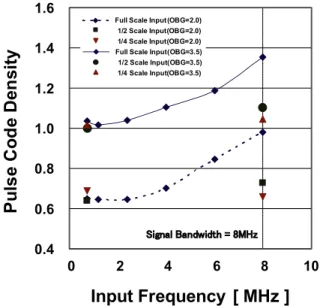
Another critical characteristics of the DAC is uncer- tainties in the edge of DAC pulse caused by clock jitter [51]
as mention in Sect. 2.1. Assuming that DAC pulse is NRZ, the jitter noise power including DAC output is estimated as following process as shown in Fig. 30.
At first, we have to derive jitter pulse power whose vari- ation and quantization step areσandΔ, respectively.
The jitter power in one bit change of DAC(Nj) is calcu- lated as following equation [52].
Nj= Δ
2 2
σ Ts
2
(24) As the jitter power(Nj) is output proportional to the ab- solute bit change of the DAC, we have to estimate the pulse code density of DAC Code. In general, it is difficult to de- rive the code density by theoretical equations. True value of the density should be derived from circuit simulations.
Figure 31 shows pulse code density dependency against input frequency, input signal amplitude and Out- Band-Gain (OBG) of NTF. In this case, 3rd-order modulator with 8 MHz-BW and 4-bit NRZ DAC was used for the sim- ulation. It is obvious that the pulse code density becomes larger when input frequency becomes higher.
The dependency to input amplitude doesn’t appear when the input frequency is lower. However the density depends on the input amplitude when the input frequency is close to the signal bandwidth. Moreover, the density is
Fig. 31 Pulse code densities from simulations.
strongly depends on the OBG. It is almost proportional to the OBG. Thus we have to make OBG as small as possible in order to realize a less sensitive modulator against clock jitter [29].
Nj= Δ
2 2
Tσs
2
OS R ×PCD (25)
If the spectrum of the pulse code density is almost flat (this assumption works out when the clock source has wider loop bandwidth than bandwidth of the modulator), the jitter noise power in DAC represents as above equation.
Here, OSR is oversampling ratio and PCD is pulse code density, respectively.
If the clock source doesn’t have enough bandwidth to make pulse code density flat, the pulse code has larger low frequency component generated by the feedback effect of the modulator. Thus the power spectrum input signal would have a wider skirt due to the low frequency component of the pulse code. Related analysis can be seen in Ref. [53], whose result is almost same as our estimation.
Switched Capacitor DAC(SC-DAC) is a dominant countermeasure against the clock jitter [97], [98], because the total charge within one feed back period is determined by the same way of a switched capacitor circuit. However, it demands the much higher GBW of amplifiers for the in- tegration as compared with the case using the current DAC.
Thus the method is mainly applied to CTDSMs with rela- tively low sampling frequency.
Using 1-bit Finite Impulse Response DAC is interest- ing way to achieve both high linearity and jitter insensitivity [99]. Very recent report shows its potential, whose FOM reaches 110 fJ/conv. with SNDR of 78 dB and 1.92 MHz of BW [100].
In this secsion we discuss mainly about a current steer- ing DAC because we have several design experiences of the modulator with such a type of DAC. However, this type of
Fig. 33 Passive summing network for Gm-C configuration.
DAC is noisier than a resistor DAC. Thus, the current DAC is preferable for a modulator with SNDR below 75 dB and bandwidth up to 10 MHz. The resistor DAC should be used for a modulator with both very wide signal bandwidth and high SNDR. The drawback to use resister DAC would be generation of larger harmonic distortion due to parasitic ca- pacitance at switching.
3.5 Signal Adder
In the low distortion architecture as shown in Fig. 12(b), adding signals at the input of quantizer is essentially needed.
So far, a signal adder using a opamp (shown in Fig. 32(a)) is commonly used. However the use of an opamp is to in- crease the power dissipation and occupies extra chip area.
Thus the passive adder using resistor (shown in Fig. 32(b)) is more preferable regarding less power and chip area [33].
There are two drawbacks on using the resistor adder.
One is the decrease of the signal dynamic range to about half. The other is that the adder is sensitive to kick back noise of the quantizer. The first drawback is not so severe because the input of the quantizer is not critical point of the SNR. The second drawback is easily avoided by using preamp in front of the quantizer.
Figure 33 shows the passive summing network for Gm- C configuration of the integration path [102]. In this case, the drawback is needs of considerably largeRLorCF1−4in order to pass low frequency component through summing network for stable operation.
3.6 Quantizer
Generally, it has been said that performances of delta-sigma modulators are not sensitive to the non-idealities of the quantizer.
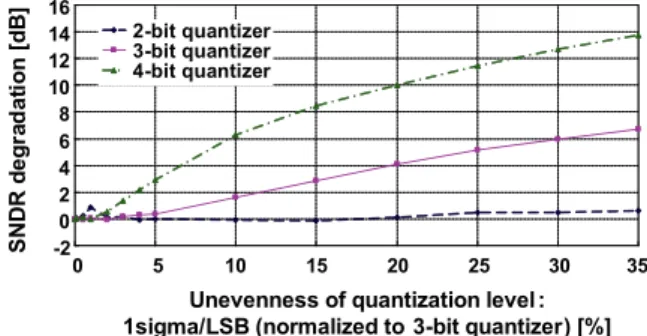
However, unevenness of the quantization levels causes harmonic distortions when there is a strong correlation be- tween an input signal and output codes. Therefore, multi-bit
Fig. 34 MATLAB Simulation results of SNDR degradation with different quantizer.
Fig. 35 Calibration scheme of the quantizer.
flash ADC more likely causes harmonic distortions. More- over, the harmonic distortions are not shaped cleanly, in case that a lower order NTF is used, Thus the unevenness tends to cause larger harmonic distortions when we use lower order modulator.
Figure 34 shows a MATLAB simulation of the effect of the quantization level unevenness. Unevenness is obtained as a worst case of 100 trials. SNDR degradation of 3rd-order filter & 3-bit quantizer is larger than that of 5th-order filter
& 3-bit quantizer and 3rd-order filter & 2-bit quantizer.
In order to make the gain bandwidth as high as pos- sible, it is essential to realize a quantizer operating higher sampling rate with small area and power consumption.
Thus, to use the smallest gate size transistor in the quantizer is inevitable.
This approach means that the unevenness of quantiza- tion level reaches up to 40%. Acceptable level of quantiza- tion level unevenness in this development of using 3rd-order filter & 3-bit quantizer is about 8%. Introduction of some calibration scheme is essentially needed.
Figure 35 shows the block diagram of the calibration circuit for comparator mismatch. In calibration mode, the inputs of the buffer are shorted and the offset current of the buffer is controlled so that the probability of “High” at the comparator output is close to 50%. The digital filter in the feedback path effectively removes the effect of noise gener- ated by comparator.
It is significant to use preamp buffer, because it de- crease not only the offset voltage of the comparator but also kick back noise effect of the comparator. Other dominant way to reduce distortion and power of quantizer is to use the so-called tracking quantizer [29], [43], [44], which predicts next input signal range of the quantizer according to recent
for medium or low speed modulators.
4. Tuning Method
In contrast to switched capacitor delta-sigma modulator (DTDSM) whose NTF and STF are determined by the ca- pacitance ratio, that of CTDSM is sensitive to absolute value of integrator components, such as resistors, capacitors and PVT variation of transistors. Thus, tuning system to control the NTF of CTDSM is inevitably needed.
It has been known well that the tuning method using PLL and AGC loop controls the frequency characteristics of the Gm-C filter very accurately [45]–[47].
However, the drawback of this method is to operate the system continuously, because the characteristic of the Gm- C filter is sensitive to temperature. This drawback is not al- lowable for the use in mobile systems. While, OTA-C filter using opamps for integration is not so sensitive so that it al- lows one time tuning of the filter performance. The required performance of the system is to determine the RC-time con- stant accurately.
The relaxation oscillator using voltage-averaging feed- back is quite suitable for the system. The schematic of the oscillator is depicted in Fig. 36 [48].
The relaxation oscillator only depends on the RC time constant because of the voltage averaging feedback (VAF) concept.
In Fig. 36, the oscillation waveform underR1Ris Vosc1,2(t)=Vdd
1−e−RC1t
. (26)
VAF loop equalizes the averaged waveform with the refer- ence generated by the resistive divider ofVddas
1 Tosc
T 0
Vosc1,2(t)dt=Vre f. (27)
Finally, we obtain the following simplified equation.
(1−α)Tosc
RC
=1−e−(ToscRC),where α= Vre f
Vdd
. (28) Equation (28) indicates that the oscillation period (Tosc) only depends on the RC constant ifαis constant.
In this case, it is easy to make the variation of the os- cillation frequency within±1%. The oscillation frequency is measured using a counter driven by a reference clock and the RC time constants of the modulator are set according to the measurement result [42].
An alternative of the method is to calibrate zero posi- tion by injecting tone whose frequency is equal to ideal zero position [60]. Figure 38 shows the block diagram of the tun- ing system with zero tone injection. The zero tone is injected
Fig. 36 Circuit schematics of the relaxation oscillator for RC-constant tuning.
Fig. 37 Block diagram of tuning system with zero tone injection.
to the feedback loop and zero components at the quantizer output is extracted by correlating with the tone. The RC constant of the loop filter is set so that the zero components including the digital output are minimized.
5. Design Methodology
In this section, we compare two design methodologies. One is conventional one, which use a transfer function in classi- cal filter theory as NTF. The other is new and much more flexible way, which uses a simulated annealing method to fix the transfer function of NTF. At the same time, the new method determines whether the system is stable or not by using s-z transform with step response matching.
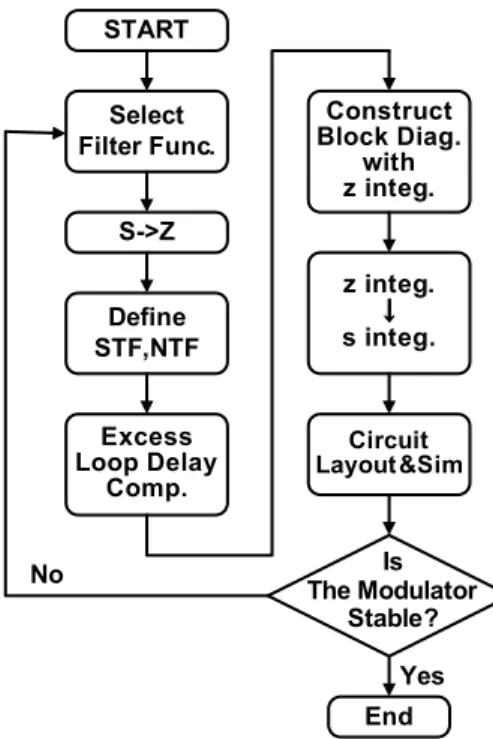
Figure 37 depicts the conventional design flow chart of CTDSM. At first, the filter prototype of NTF is cho- sen among the filter of classical theory [49], [50]. Inverse Chebyshev filters are frequently used for NTF prototype be- cause those filter maximize the decrease of the quantiza- tion noise by introducing the zero in the signal band. Next, STF(z) and NTF(z) are derived from the prototype filter transformed in z-domain. We have to compensate the ex- cess loop delay by changing NTF(z) slightly as detailed in Sect. 3.2.
Next, the transfer function of the NTF is mapped to the block diagram as shown in Fig. 39(a). Then the final transform is done so that discrete integrators are changed to those of the continuous type as shown in Fig. 39(b).
Fig. 38 Conventional design flow chart of CTDSM.
Fig. 39 Block diagram of integration path.
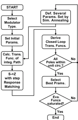
Fig. 40 Advanced design flow chart of CTDSM with simulated annealing and step response matching.
The top issue of conventional design flow is that it does not ensure the loop stability of the modulator even if the ex- cess loop delay compensation is done [15]–[17], because the discrete model using in this design method does not preserve the continuous time response from DAC output to the input of quantizer. A design cycle re-run frequently occurs, which bothers circuit designers. Another issue of the design is that the less flexibility of the NTF. The filter type of the NTF is limited within classical filter theory, which also limits the FOM of the modulator.
So far, optimization flows based on the convex opti- mization have been reported [101]. However the abilities are not enough for exploring circuit parameters beyond the classical filter theory with keeping the loop stability.
In fact, more advanced filter design method is essential in order to pursue further improvement of FOM.
Figure 40 illustrates more advanced design flow of CTDSM. The most distinctive advantage of the new design flow is that it can determine the loop stability of the modula- tor very accurately. Therefore, we can explore a much wider design space for the integration path. This fact give us the chance to apply quite new transfer functions for the inte- gration path, which are not limited by classical filter theory such as Chebyshev filters. In this case we use a simulated annealing method for the exploration.
At first, we have to prepare the model of integration path that consider the parasitic effects and non-ideality, such as parasitic capacitance, resistance and excess phase shift of the integrator.
Next, several initial set of the parameters are given to
Fig. 41 Zero order hold S-Z transformation.
the model to start optimization of the modulator. In order to realize the accurate determination of the stability in z-plane, we have to match the time response of the discrete model of the integration path to that of continuous filter.
It means that the s-z transformation has to preserve the step response of the integration path in case of using the NRZ-DAC. If we use the RZ-DAC s-z transformation has to preserve the pulse response of the integration path.
In this case, we use the NRZ-DAC. Thus, we transform the model of integration path to that of discrete model by zero order hold s-z transformation, which preserves the step response of continuous model as shown in Fig. 41.
In case of using the NRZ-DAC, the z-domain model in- herits the stability of the continuous model, as long as those step responses are matched to that of the continuous circuit exactly. (The mathematical analysis of this method is seen in Ref. [22]).
The closed loop responses are derived from discrete model of the integration path, whose stability exactly re- flects that of the original modulator. Thus the original con- tinuous modulator should be stable if all poles of the discrete model are within the unit circle.
Actually, similar design approach is seen in Ref. [54].
However the approach shows only simulation results. The effectiveness was not verified by the test chip. It is distinc- tive for our approach to verify the optimization result by the test chip discussed below.
Among modulates under test, the stable parameter set showing the best performance are selected so that the best parameter should be next seed of parameters that was gen- erated by the simulated annealing method.
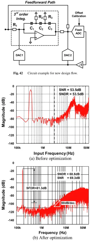
Until the best performances are saturated, this design cycle runs over. Figure 42 shows the design example for the new design method, whose integral path(H(s)) has a incom- plete 3rd order integral function as follows.
H(s)=
−s2(C1C2+C2C3+C3C1)R2R3+s((C1+C2)R2+(C2+C3)R3)+1 s3C1C2C3R1R2R3
(29) In this case, if the selection of the parameter set in the Eq. (29), the order of the integration is close to 1. Thus the SNDR of the modulator degrades. In order to maximize the SNDR, we have to explore the design space of the integral function as wide as possible with keeping the stable oper- ation of the modulator. Figure 43 shows the comparison
Fig. 42 Circuit example for new design flow.
Fig. 43 Optimization result of 3rd order-CTDSM.
results between before and after optimization. The noise transfer function after optimization as shown in Fig. 43(b) shows 3rd order integral as compared with that before opti- mization shown in Fig. 43(a) whose noise transfer function shows only 1st order integral.
The new design method can improve SNDR of 15.1 dB
not simulation result but measured one. The measured chip performances are summarized in Table 2. It is remarkable that the measured FOM was less than 100 fJ/conv., even if we use the very simple and incomplete 3rd order integral filter.
6. State-of-the-Art Survey
6.1 Performance Comparison
The origin of CTDSMs is very old. It is interesting that its history is longer than that of discrete type modulator [5].
So, there have been a huge number of modulators pub- lished for various specific applications, for multimode oper- ation, realizing higher signal bandwidth, minimizing FOM, pursuing small area, achieving higher SNDR, and so on.
Thus, in this section, various type CTDSMs are cate- gorized based on their characteristics.
At first, the most distinctive characteristic of CTDSM is that it has wider signal bandwidth than that of DTDSM.
So, Table 3 summarizes recent CTDSMs whose signal band- widths are higher than 1 MHz. Here modulators are classi- fied as follows: Normal CT means a modulator with sin- gle feedback loops, Time-Base CT means one which con- verts the input signal to phase signal by using a voltage controlled oscillator, Cascaded CT means cascaded Normal CTs and DTCT Hybrid means one a part of which is com- posed of switched capacitor circuit. FOM1 and FOM2 are determined by following equations.
FOM1= PowerDissipation
2(S NDR−1.76)/6.02×DOR (30) FOM2=S NDR+10 log10
Bandwidth PowerDissipation
(31) DOR: Digital Output Rate of the Modulator
Figure 44 also summarizes those performances. The slash line in the figure indicates same level of the perfor- mance provided that an increase of SNDR twice needs 4 times power dissipation.
Currently, Normal-CTs almost rank high. Fundamental strategies for realizing high efficiency are to use multi-bit DAC to alleviate the influence of clock jitter, to use DWA to move the non-linearity of the DAC to high frequency region.
In addition, over 3 order loop filters are used for lower- ing oversampling ratio to minimize the power consumption.
The single opamp resonator is quite suitable not only for lowering the power but also lowering the circuit area [33],
Fig. 44 Performances of recent CTDSMs with FOM1.
[42].
On the other hand, Time-Base-CTs are getting increase their performances, because those CTDSMs are less insen- sitive to the clock jitter. This feature makes Time-Base-CTs suitable to realize the modulator with higher bandwidth, which is confirmed by Fig. 45.
There are two types of Time-Base-CTs. One has a feedback loop (as shown in Figs. 46(a)–(c)) and the other doesn’t have it (as shown in Fig. 46(d)).
The former types feed back the timing information so that jitter phase noise is suppressed by the feed back effect.
Thus those types are less sensitive to the jitter.
The first Time-Base-CTs using VCO quantizer is shown in Fig. 46(a), which is based on the idea that the or- der of the modulator increases by one as the VCO acts an integrator.
The drawback to use the VCO is its non-linearity. An alternative to use the VCO quantizer is to use PWM-based quantizer as shown in Fig. 46(b). Actually, the quantizer im- proves the linearity. However the quantizer introduces the limitation of the dynamic range [87].
Fig. 45 Performances of recent CTDSMs with FOM2.
Fig. 46 Architectures of time base CTDSMs.
The third generation of the closed loop Time-Base CT is using a self-oscillation loop so called time-encoding quan- tizer (TEQ) as shown in Fig. 46(c). This quantizer acts as self-oscillating PWM [67].
The latter types differentiate the phase information to derive the frequency information, which reduces the phase noise. It is a big advantage of Time-Base-CTs as compared with Normal-CTs [61], [88]. Incorporating recent multi- phase VCO techniques [89], these CTs easily improve both resolution and FOM.
Moreover, they quite go well with advanced nm pro- cesses because it is easy to realize a higher frequency os- cillation and a smaller timing resolution. So those types of architecture will be applicable to reconfigurable wireless communication system at an early date.
Especially, open-loop Time-Base-CTs are quite attrac- tive due to its compactness, even if there are some draw- backs: they have strong nonlinearity arise from the charac- teristics of VCO, sensitivities against supply noise or PVT variations are usually high to be compensated, phase accu- racies of the VCO outputs are not enough to make spurious small. Those drawbacks should be compensated by some digital calibration method because huge numbers of transis- tor gates are easily useful in advanced nm process.
On the other hand, CTDSMs with cascaded structure (Cascaded CTs) doesn’t show better performance as com- pared with other type CTDSMs. It is because the cascaded structure is more sensitive to mismatches of modulators that the 1st order quantization noise from the first stage leaks if there is a mismatch of frequency characteristics between cascaded stages. Other suitable application of CTDSM is a bandpass modulator, because continuous modulator dis- sipate less power consumption that of DTDSM. Moreover, anti-alias filter in front of the modulator is not needed. Per- formances of several recent bandpass CTDSMs are summa- rized in Table 4 and Fig. 47.
So far, quadrature type for low-IF receiver shows supe- rior SNDR and FOM as compare with normal type bandpass CTDSMs, because center frequency of the quadrature mod- ulator is much lower than that of the normal type bandpass modulator due to its low-IF application. It is certain that a filter that has lower cut offfrequency easily realizes a higher Q factor. Thus the quadrature bandpass modulator tends to be higher SNDR and lower FOM.
One of other interest approach for wireless communi- cation is to combine CTDSMs with a mixer so that the loop
Fig. 47 Performances of recent BP-CTDSMs with FOM1.
Table 5 Performances of reconfigurable CT and DTDSMs.
filter of the CTDSM is used for a image rejection [110], [111]. Especially, Ref. [111] has an unique circuit configu- ration not processing IQ-signals but 3-phase signals, which also decreases circuit area and power consumption.
6.2 Reconfigurable CTDSMs
The most popular application of CTDSMs is wireless com- munication. Recent wireless system requires multi-mode operation. So, CTDSMs should have a reconfigurability to change signal bandwidth and SNR corresponding to plural wireless communication standards. Here, we call this type of CTDSMs as “Reconfigurable CTDSMs”.
It should be discussed which is suitable for reconfig- urable wireless system, CT or DTDSM.
Table 5 compares the performances of reconfigurable CT and DTDSMs and Fig. 48 visualizes their FOM1 against the signal bandwidth.
Fig. 48 FOM1 of reconfigurable CT & DTDSMs against signal band width.
Fig. 49 Comparison of sensing method for driver current.
It is obvious that CTDSMs has better FOM in higher signal bandwidth, because DTDSMs need much larger power for settling the output of the amplifier in a shorter clock period. However, the FOM1 of CTDSMs is larger than we expected, because almost reconfigurable CTDSMs uses 1 bit SC-DAC in order to prevent harmonic distortions.
Thus, the key point of the further decrease of FOM1 is to suppress the harmonic distortion without using the 1 bit SC- DAC.
6.3 Expansion of Application Field
It is interesting fact that CTDSM expands its application field widely. One is a sensor application and the other is driver controller, such as DC-DC or motor controller [81]–
[85].
So far, series resistor is used for sensing a current flow- ing through inductor in DC-DCs or motor drivers as shown in Fig. 49(a). However, the voltage across the series resistor is usually very small. Thus a high resolution ADC is needed to sense the inductor current.
Advanced way to sense the current by using CTDSMs are based on the following equation.
Vind=LdIind
dt ⇔Iind= 1 L
Vinddt (32)
Fig. 50 1st order 1 bit CTDSM for current sensing.
Table 6 Performances of CT & DTDSMs for voice coding.
That is, the inductor current is derived by the integral of voltage across the inductor. CTDSM is quite suitable to per- form Eq. (32), because the input voltage is integrated and quantized in the CTDSM. Thus 1st order CTDSM is used as shown in Fig. 49(b) [85].
The 1st order 1 bit CTDSM is unique architecture on the point that the performances of the modulator are insen- sitive to its opamp performances, such as DC gain or GBW [86]. It is because that the error of the quantizer will be com- pensated at next comparison as long as the principle of the charge conservation is kept in the integrator. Especially, this feature is suitable for sensing current.
Figure 50 shows the 1st order 1 bit CTDSM for cur- rent sensing. Although the very simple one stage integrator is used, output results is not affected by non-idealities of the integrator, such as low gain or narrow GBW. Note that CTDSM with voltage input is not allowed to use such a low gain integrator because low gain amplifier stirs the virtual ground, which causes the degradation of the INL.
Other potential application of the CTDSM is low volt- age operation due to its switchless architecture. The lowest supply voltage is down to 0.5 V [103].
Finally, the application area of the CTDSM is expanded to that of the audio where discrete type modulators are reign- ing. Table 6 summarizes performances of recent CT &
DTDSMS for voice coding.
It is amazing that the lowest FOM of CTDSM [104]
is almost equal to that of DTDSM [105]. The biggest is- sue of the CTDSM for improving the FOM is the effect of the clock jitter, however the problem is now overcoming to some extent. Thus, it is certain that the application field of the CTDSM will go over those of DTDSMs.
7. Conclusions
The continuous-time delta-sigma modulator is the most in- teresting circuit configuration, because it is a mixed signal
methodology is also detailed.
The surveys of the technology convince us that the ap- plication field of CTDSM will be expanded in the future as the downsizing of the CMOS process goes toward a low voltage and a high-speed operation. Improvements of the circuit performances are still continuing.
The author would be pleased if the reader have interest in CTDSMs and join the development those.
Acknowledgment
The author would like to express his gratitude to the mem- bers of the Panasonic delta-sigma ADC design group, espe- cially to Mr. K. Matsukawa, Dr. K. Obata, Mr. Y. Mitani, Mr. M. Takayama, Dr. Y. Tokunaga, Dr. T. Morie and Mr. S. Sakiyama. They offered some materials for prepa- ration of this paper. The author is also grateful to the Asso- ciate Editor and the anonymous reviewers for their construc- tive and valuable comments and suggestions to improve the quality of this paper.
References
[1] H. Inose, Y. Yasuda, and J. Murakami, “A telemetering system by code modulation —Δ-Σmodulation,” IRE Trans. Space Electron.
Telemetry, vol.8, pp.204–209, Sept. 1962.
[2] D.L. Fried, “Analog Sample-Data Filters,” IEEE J. Solid-State Cir- cuits, pp.302–304, Aug. 1972.
[3] I.A. Young, P.R. Gray, and D.A. Hodges, “Analog NMOS sampled data recursive filters,” Proc. Int. Solid State Circuits Conference, pp.156–157, Philadelphia, Feb. 1997.
[4] B.J. Hosticka, R.W. Brodersen, and P.R. Gray, “MOS sampled data recursive filters using switched capacitor integrators,” IEEE J. Solid-State Circuits, vol.SC-12, no.6, pp.600–608, Dec. 1977.
[5] J.-P. Petit, “Digital transmission system with a double analog inte- grator delta sigma coder and a double digital integrator delta sigma decoder,” U.S. Patent 4,301,446, June 1980.
[6] R. Schreier and B. Zhang, “Delta-sigma modulators employing continuous-time circuitry,” IEEE Trans. Circuits Syst. I, vol.43, no.4, pp.324–332, April 1996.
[7] I. Galton, “Delta-sigma data conversion in wireless transceivers,”
IEEE Trans. Microw. Theory Tech., vol.50, pp.302–315, Jan. 2002.
[8] J.M. de la Rosa, “Sigma-delta modulators: Tutorial overview, de- sign guide, and state-of-the-art survey,” IEEE Trans. Circuits Syst.
I, vol.58, no.1, pp.1–21, Jan. 2011.
[9] L. Breems and J. Huijsing, Continuous-Time Sigma-Delta Modu- lation for A/D Conversion in Radio Receivers, Norwell, Kluwer, MA, 2001.
[10] M. Ortmanns and F. Gerfers, Continuous-Time Sigma-Delta A/D Conversion: Fundamentals, Performance Limits and Robust Im- plementations, Springer, New York, 2006.
[11] V. Peluso, M. Steyaert, and W. Sansen, Design of Low- Voltage Low-Power CMOS Delta-Sigma A/D Converters, Nor-
[16] S. Pavan, “Excess loop delay compensation in continuous-time delta sigma modulators,” IEEE Trans. Circuits Syst. II, Exp. Briefs, vol.55, pp.1119–1123, Nov. 2008.
[17] M. Keller, A. Buhmann, J. Sauerbrey, M. Ortmanns, and Y.
Manoli, “A comparative study on excess-loop-delay compensation techniques for continuous-time Sigma-Delta modulators,” IEEE Trans. Circuits Syst. I, Reg. Papers, vol.55, pp.3480–3487, Dec.
2008.
[18] R. Schreier and M. Snelgrove, “Bandpass sigma-delta modula- tion,” IET Electron. Lett., vol.25, pp.1560–1561, Nov. 1989.
[19] P.H. Gailus, “Method and arrangement for a sigma delta converter for bandpass signals,” U.S. Patent 4 857 828, Aug. 1989, filed Jan.
28 1988.
[20] S. Jantzi and W. Snelgrove, “Bandpass sigma-delta analog-to- digital conversion,” IEEE Trans. Circuits Syst., vol.38, pp.1406–
1409, Nov. 1991.
[21] S. Jantzi, W. Snelgrove, and P. Ferguson, “A fourth-order band- pass sigma-delta modulator,” IEEE J. Solid-State Circuits, vol.28, pp.282–291, March 1993.
[22] J. Engelen and R. van de Plassche, BandPass Sigma-Delta Modu- lators: Stability Analysis, Performance and Design Aspects, Nor- well, Kluwer, MA, 1999.
[23] R.T. Baird and T. Fiez, “Linearity enhancement of multibitΔΣA/D and D/A converters using data weighted averaging,” IEEE Trans.
Circuits Syst. II, Analog Digit. Signal Process., vol.42, pp.753–
762, Dec. 1995.
[24] A. Yasuda, H. Tanimoto, and T. Iida, “A third-order-modulator us- ing second-order noise-shaping dynamic element matching,” IEEE J. Solid-State Circuits, vol.33, pp.1879–1886, Dec. 1998.
[25] R. van Veldhoven, “A triple-mode continuous-timeΔΣmodulator with switched-capacitor feedback DAC for a GSM-EDGE/ CDMA2000/UMTS receiver,” IEEE J. Solid-State Circuits, vol.38, pp.2069–2076, Dec. 2003.
[26] R. Schreier, “An empirical study of high-order single-bit delta- sigma modulators,” IEEE Trans. Circuits Syst. II, vol.40, no.8, pp.461–466, Aug. 1993.
[27] Page 108 in reference [14].
[28] A.B. Williams and F.J. Taylors, Electronic Filter Design Hand- book, McGraw-Hill New York, 1988, ISBN 0-07-070434-1.
[29] L. Dorrer, F. Kuttner, P. Greco, P. Torta, and T. Hartig, “A 3- mW 74-dB SNR 2-MHz continuous-time delta-sigma ADC with a tracking ADC quantizer in 0.13-μm CMOS,” IEEE J. Solid-State Circuits, vol.40, no.20, pp.2416–2427, Dec. 2005.
[30] K. Yamamoto, et al., “Delta/sigma TYPE A/D converter,”
JP63039216(A)
[31] L. Ping, “Oversampling analog/digital converters with finite ze- ros in noise shaping functions,” IEEE International Symposium on Circuits and System, pp.1645–1648, June 1991.
[32] G. Mitteregger, C. Ebner, S. Mchnig, T. Blon, C. Holuigue, and E.
Romani, “A 20-mW 640-MHz CMOS continuous-timeΔΣADC with 20-MHz signal bandwidth, 80-dB dynamic range and 12-bit ENOB,” IEEE J. Solid-State Circuits, vol.41, pp.2641–2649, Dec.
2006.
[33] K. Matsukawa, Y. Mitani, M. Takayama, K. Obata, S. Dosho, and A. Matsuzawa, “A fifth-order continuous-time delta-sigma modu- lator with single-opamp resonator,” IEEE J. Solid-State Circuits,