Electronic Properties of sp2 Carbon Networks
with Defects and Interfaces
著者
Maruyama Mina
year
2017
その他のタイトル
欠陥や境界を有する二次元sp2炭素ネットワークの
電子物性
学位授与大学
筑波大学 (University of Tsukuba)
学位授与年度
2016
報告番号
12102甲第8031号
URL
http://hdl.handle.net/2241/00147776
Electronic Properties of sp
2
Carbon Networks with
Defects and Interfaces
Mina Maruyama
Electronic Properties of sp
2
Carbon Networks with
Defects and Interfaces
Mina Maruyama
Doctoral Program in Nano-Science and Nano-Technology
Submitted to the Graduate School of
Pure and Applied Sciences
in Partial Fulfillment of the Requirements
for the Degree of Doctor of Philosophy in
Science
at the
Abstract
Graphene maintains premier position in the field of nanoscience and nanotechnology because of its simple geometric structure, which allows graphene a precursor for var-ious nanoscale derivatives being applicable for future electronic devices by attaching and implanting imperfections in its hexagonal network. Imperfections, for instance, edges, defects, and interfaces, lead to various topological networks, resulting in in-teresting electronic properties which are absent in bulk graphene. Theoretical and experimental works corroborated that the strong correlation between the geomet-ric and electronic properties of these two-dimensional sp2 carbon networks. In this thesis, we aim to design and investigate novel two-dimensional carbon networks consisting of sp2 carbon atoms which results in unusual electronic structures by first-principles total-energy calculations based on density functional theory.
We investigate geometric and electronic structures of a two-dimensional stable carbon allotrope consisting of pentagonal rings. We found that the sp2 carbon sheet has a slightly higher total energy than C60 and retains its planar structure up to 1000 K, indicating that the sheet is both energetically and kinetically stable. The electronic structure of the sheet is found to be a metal with a flat dispersion band at the Fermi level, leading to spin polarization on the sheet. The polarized electron spin is ferromagnetically aligned and extends throughout the sheet with a spin moment of 0.62 µB/nm2.
We investigate the geometric and electronic structures of porous graphene net-works consisting of phenalenyl and phenyl groups, which are connected alternately with C3 symmetry via single bonds to form a honeycomb network. The networks possess both Dirac cones and Kagome flat bands near the Fermi level because the phenalenyl and phenyl form hexagonal and Kagome lattices, respectively. Because of the large spacing between phenalenyl units, the networks possess very slow mass-less electrons/holes at the Fermi level, the Fermi velocity of which is a hundred times lower than that of graphene, leading to spin polarization on the networks with an-tiferromagnetic and ferromagnetic ordering as their stable states. Our calculations show the antiferromagnetic state is the ground state whose energy is lower by 14 meV than that of the ferromagnetic state. We also demonstrate that the electronic structure of the two-dimensional networks is sensitive to the rotation of the phenyl unit connecting phenalenyl units.
We study the energetics and magnetic properties of two graphene dots with tri-angular shapes embedded in an h-BN sheet. Our first-principles total-energy calcu-lations show that the graphene dots in h-BN prefer the closest inter-dot spacing as their ground state arrangement. Furthermore, total energy of the heterosheet mono-tonically increases with increasing inter-dot spacing and immediately saturates at
0.21 and 0.12 eV for NC and BC borders, respectively, at the inter-dot spacing of 7.5 ˚A. We also find that ferrimagnetic spin polarization occurs on each graphene dot with S = 1/2 magnetic moment, which are aligned in singlet and triplet ar-rangement between two dots under inter-dot spacings of 5.0 ˚A or larger. The spin polarization energy saturates at approximately 100 meV per graphene dot at an inter-dot spacing of 8.0 ˚A. The spin–spin interaction J prefers an antiparallel spin coupling to a parallel one with an energy of 25 meV at an inter-dot spacing of 5.0 ˚
Contents
1 Introduction 1
2 Calculation Method 13
2.1 Density functional theory . . . 13
2.1.1 Hohenberg-Kohn theorems . . . 14
2.1.2 Kohn-Sham equation . . . 17
2.1.3 Local density approximation . . . 17
2.1.4 Generalized gradient approximation . . . 18
2.1.5 Spin density functional theory . . . 18
2.2 Bloch’s theorem . . . 19
2.3 Plane-wave basis set . . . 19
2.4 Pseudopotential . . . 20
2.4.1 Norm-conserving pseudopotentials . . . 21
2.4.2 Ultrasoft pseudopotential . . . 21
2.5 Effective screening medium method . . . 23
3 Two-Dimensional sp2 Carbon Network of Fused Pentagons: All Carbon Ferromagnetic Sheet 27 3.1 Introduction . . . 27
3.2 Energetics and optimized structure . . . 28
3.3 Electronic strucutre . . . 30
3.4 Stacking structure . . . 34
3.5 Conclusion . . . 34
4 Coexistence of Dirac cones and Kagome flat bands in a porous graphene 35 4.1 Introduction . . . 35
4.2 Energetics and optimized structures . . . 36
4.3 Electronic structures . . . 38
4.4 Magnetic properties . . . 41
4.5 Energetics and magnetic property of phenalenyl dimer connected via phenyl . . . 45
5 Magnetic Properties of Graphene Quantum Dots Embedded in h-BN Sheet 49 5.1 Introduction . . . 49 5.2 Structural model . . . 50 5.3 Energetics . . . 50 5.4 Magnetic properties . . . 53 5.5 Electronic structures . . . 54 5.6 Conclusion . . . 55 6 Conclusion 63
Chapter 1
Introduction
Carbon atom are known to form three orbital hybridizations, sp, sp2, and sp3, lead-ing to various in its covalent bonds [Figure 1.1]. Accordlead-ingly, carbon possesses various allotropes which cover all dimensionality with metallic or insulating prop-erties depending on their orbital hybrization. For instance, carbyne, graphite, and diamond are representative allotropes consisting of C atoms with sp, sp2, and sp3 hybridizations, respectively [Figure 1.2]. Graphite has a stacked layered structure of honeycomb sheets consisting of C atoms. Each C atom is connected to three ad-jacent atoms via σ covalent bond with a length of 1.42 ˚A and angle of 120◦ forming two-dimensional (2D) network. On the other hand, π states are distributed normal to the layer and are weakly overlap within and between layers, inducing a metallic electronic structure of graphite [Figure 1.3] [1]. In contrast to graphite, diamond is an insulator with a bandgap of 5.5 eV and a hard material with 10 Mohs. These electronical and mechanical properties are ascribed to its three-dimensional network of tetrahedrally, bonded C with sp3 hybridization.
Structural flexibility of covalent bonds of C atoms allows us to have other al-lotropes. Figure 1.4 shows representative examples of novel carbon allotropes with nanoscale sizes. In 1985, Kroto, Smalley, and Curl have predicted the presence of hollow-cage carbon cluster, fullerene, in mass spectra of carbon cluster, in which they observed remarkable peak at the cluster size of 60 [2]. By combing the experimental fact and the structure of a soccer ball, they deduced the C60 cluster consisting of 12 pentagonal and 20 hexagonal rings with Ih symmetry. Following the macroscopic production of C60 and other large fullerenes, the Ih cage structure of C60 has been confirmed [3]. Soon later, in 1992, Iijima has discovered tubular forms of graphitic carbon with nanometer diameter (carbon nanotube: CNT) using transmission elec-tron microscope [4]. In the case, owing to the boundary condition imposed on the electronic structure of monolayer graphite, CNT is either a metal or semiconductor depending on their atomic arrangement along its circumference [5, 6]. Furthermore, in 2004, graphene, a constituent atomic layer of graphite, has been exfoliated from bulk graphite by Novoselov and Geim [7, 8]. As has been already mentioned, the graphene has a pair of linear dispersion bands at the Fermi level (EF) and K point due to their hexagonal atomic layer network [Figure 1.5]. Following the discover-ies and synthesis of these novel carbon allotropes, they have been attracting much attention in both basic and applied sciences for the last three decades.
Ground state
2s
22p
2Excited state
2s
12p
3sp
3sp
2p
sp
2p
Figure 1.1: Electronic configurations of carbon.
Among these three novel carbon nanoallotropes, graphene is now keeping premier position in the field of nanoscience and nanotechnology because of its simple geo-metric structure, which allows graphene a precursor for various nanoscale derivatives being applicable for future electronic devices by attaching and implanting imperfec-tions in its hexagonal network. By cutting the graphene along particular direction, we can construct the graphene ribbons with nanometer width (GNR) [Figure 1.6]. In the case, the energetics and electronic structure of the GNRs are sensitive to their width and edge atomic arrangement [9]. GNRs with armchair edge become semiconductors of which band gap asymptotically decreases with increasing their widths [10]. In addition, GNR with zigzag edges possesses flat dispersion bands at EF and around the zone boundary, which are split into upper and lower branches under the infinitesimal on-site Coulomb interaction U , leading to the spin polariza-tion near the edge atomic sites [11, 12]. These flat band states are known to be the edge states which are induced by the delicate balance among the π electron transfer near the edge atomic sites.
By imposing an additional open boundary condition normal to the ribbon di-rection on GNR, we can get graphene nanoflakes or hydrocarbon molecules. The electronic structure of the graphene nanoflake also depend on its flake size and shape. The molecules are ranging from the closed shell electronic structure to the open shell electronic structure with radical spins. The energies of small graphene nanoflakes or hydrocarbon molecules can be determined using the empirical procedure which is known to be the Huckel’s rule: The hydrocarbon molecules containing 4k + 2 C atoms are energetically stable where k is integer numbers. These molecules basically possess the finite energy gap between highest occupied (HO) and lowest unoccupied (LU) states, which is inversely proportional to the size of the molecule, although the
sp
sp
2sp
3Graphite
Diamond
Carbyne
Figure 1.2: sp, sp2, and sp3 hybridized covalent bonds and carbon allotropes con-sisting of their bonds, respectively.
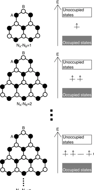
detailed electronic structure depends on their C-C network topology. On the other hand, the hydrocarbon molecules with triangular shape occasionally possess open-shell electronic structures possessing the number of half-filled zero energy modes with non-bonding nature associated with the sublattice imbalance of their networks [Figure 1.8] [13, 14]. For instance, phenalenyl is the smallest example of the hydro-carbon molecule with radical spin. It should be noted that these open shell graphene nanoflake are energetically unstable due to the partially filled electron state at EF, causing to the large electron energy.
In addition to the periodic and open boundary conditions, the topological defects and interfaces with other 2D materials also terminate or modulate the π electron networks of the GNRs or graphene nanoflakes as the other possible boundary condi-tions on the sp2 C networks [Figure 1.9] [15]. The topological line defects consisting of octagonal and a pair of pentagonal rings can terminate the π electron states near EF leading to the localized state around the topological line defect as in the case of edge state in the GNR with zigzag edges. The topological defect is inherent in the domains boundary of the polycrystalline graphene experimentally synthesized [Figure 1.10] [16]. Interfaces between graphene and other layered materials also act as the open boundary condition on the graphitic π network. Early theoreti-cal theoreti-calculations demonstrated that the electronic structure of the interface between graphene and hexagonal boron nitride (h-BN), which is honeycomb sheet consisting
Figure 1.3: Electronic structures of graphite [1]. The energy is measured from that of the Fermi level.
0D
1D
2D
Figure 1.4: Geometric structures of fullerene, carbon nanotube, and graphene. of boron and nitrogen with bond length of about 1.44 ˚A, depends on the detailed atomic arrangement at the interfaces: Interfaces with zigzag arrangement leads to the interface localized states near EF with bonding and antibonding character of C and B/N atoms [Figure 1.11] [17]. In contrast, the localized state is absent at the interface with armchair shape. Furthermore, by designing the interface mor-phology, the graphene domains exhibit the spin polarization as in the cases of the graphene nanoflakes with sublattice imbalance or GNR with zigzag edges. Besides the foreign 2D materials, nanoscale vacancies also act as the boundary condition on the graphitic π networks of carbon, leading to the peculiar electron states at EF, such as an isolated flat band state or the Kagome’s flat band states at or near EF [Figure 1.12] [18].
This thesis contains three following studies about electronic properties of graphene with topological defects, vacancies, and interfaces. Before showing our calculations, in chapter 2, we review calculation methods used in this thesis. We will show the geometric and electronic structure of a 2D carbon allotrope consisting of pentag-onal rings in chapter 3. The 2D networks consisting of fused pentagpentag-onal rings is a metal with the flat dispersion band in the part of the 2D Brillouin zone leading to the ferromagnetic spin ordering throughout the sheet. We demonstrate the 2D
hydrocarbon network consisting of phenalenyl and phenyl which are alternately ar-ranged with C3 symmetry in chapter 4. The 2D hydrocarbon sheet possesses both Dirac cones and Kagome’s flat bands near EF, which are originated from the non-bonding states of the hexagonally arranged phenalenyl units and the HO state of the phenyl forming the Kagome lattice, respectively. Furthermore, the 2D hydro-carbon network also possesses spin polarization localized on the phenalenyl units. In chapter 5, we present the energetics and magnetic properties of two graphene dots (phenalenyl shape domain) embedded into a h-BN sheet. We found that fer-rimagnetic spin polarization occurs on each graphene dot aligned in singlet and triplet arrangements between two dots with the short-range spin-spin interaction J. Finally, we summarized this thesis in chapter 6.
-20
-15
-10
-5
0
5
10
15
En
e
rg
y
[e
V]
L
M
K
K
Figure 1.5: Electronic structure of graphene. The energy is measured from that of the Fermi level.
Figure 1.6: Geometric structures of graphene nanoribbon with edge angles of (a) 0◦ (armchair edge), (b) 8◦, (c) 16◦, (d) 23◦, and (e) 30◦ (zigzag edge) [9].
Figure 1.7: Electronic structure and spin moment of a graphene nanoribbon with zigzag edges. The energy is measured from that of the Fermi level [11].
NA-NB=1 A B NA-NB=2 A B Occupied states Unoccupied states E Occupied states Unoccupied states E NA-NB=n A B Occupied states Unoccupied states E n
Figure 1.8: Schematic pictures of geometries and energy levels of triangular graphene flakes.
Figure 1.9: (a) Geometric and (b) electronic structures of graphene with topological line defect consisting of pentagonal and octagonal rings [15]. The energy is measured from that of the Fermi level.
Figure 1.10: Scanning electron microscope images of graphene with grain bound-ary [16].
Figure 1.11: Contour plots of spin densities of heterosheet consisting of graphene and h-BN [17]. White, black, and gray balls denote carbon, nitrogen, and boron atoms, respectively.
Figure 1.12: Geometric and electronic structures of porous graphene networks [18]. The energy is measured from that of the Fermi level.
Chapter 2
Calculation Method
In this chapter, we present calculation methods used in this thesis. All calculations were performed using the density functional theory. This chapter is organized as follows. In section 2.1, we describe the density functional theory. To adopt the density functional theory for the crystals, Bloch’s theorem is briefly described in section 2.2. Plane wave basis set is described in section 2.3. To described interaction between electrons and nuclei, we use pseudopotential procedure which is explained in section 2.4. In the section 2.5, we describe the effective screening medium method to calculate the materials under the electric field within the density functional theory with plane wave method.
2.1
Density functional theory
The most widely used theory in the modern electronic structure calculations (with the simultaneous atomic-geometry optimization) is the density functional theory (DFT). The DFT is a principle theory of the electronic structures of atoms, molecules, and solids in their ground states, which are described using the electron density dis-tribution n(r) (Hohenberg and Kohn in 1964 [19] and Kohn and Sham in 1965 [20]). In this section, we describe two theorems, and derive self-consistent equations based on these two theorems. Approximations adopted in the equations are also explained in this section.
2.1.1
Hohenberg-Kohn theorems
The hamiltonian of N-electrons system,
H = T + U + V (2.1) = N ! i=1 " − ! 2m∇ 2 i # +1 2 N ! i̸=j e2 |ri− rj| + N ! i=1 v(ri) (2.2) T = N ! i=1 " − ! 2m∇ 2 i # (2.3) U = 1 2 N ! i̸=j e2 |ri− rj| (2.4) V = N ! i=1 v(ri) (2.5)
is corresponded to Schr¨odinger equation of
HΨ(r1,· · · , rN) = EΨ(r1,· · · , rN). (2.6) For solving the Schr¨odinger equation, electronic density n(r) can be written
n(r) = (Ψ, ˆnΨ) (2.7) = $ Ψ∗(r1,· · · , rN)ˆn(r)Ψ(r1,· · · , rN)dr1· · · drN (2.8) where ˆ n(r) = N ! i−1 δ(r− ri). (2.9) By using the n(r), an expectation of V can be written
(Ψ, V Ψ) = $ Ψ∗ % N ! i=1 v(ri) & Ψdr1· · · drN (2.10) = $ Ψ∗ %$ !N i=1 v(r)δ(r− ri)dr & Ψdr1· · · drN (2.11) = $ v(r)n(r)dr. (2.12)
Kohn-Sham theorems are presented by using these premises following. In the DFT, for an interacting N-electron system, the ground state density n(r) uniquely corre-spond to an external field v(r):
This is true whether the ground state is non-degenerate or degenerate (In the latter case any of the possible ground state densities uniquely determines the potential v(r)). (First, the proof for non-degenerate ground states will be presented:)
Let v(r) be the external potential of the system associated with ground state density n(r), total number of particles N = ' n(r)dr, Hamiltonian H and ground state Ψ and energy E,
v :H, N, n(r), Ψ, E. (2.14) Similarly, we consider a second system of v with
v′ :H′, N′, n′(r), Ψ′, E′ (2.15) where v′ ̸= v+C and Ψ′ ̸= Ψ. Then, by using the Rayleigh-Ritz variational principle E = (Ψ,HΨ) < (Ψ′,HΨ′) (2.16) = (Ψ′, (H′− V′+ V )Ψ′) (2.17) = E′+ $ [v(r)− v′(r)]n(r)dr (2.18) or E < E′ + $ [v(r)− v′(r)]n′(r)dr. (2.19) The inequality follows from the fact that Ψ′ ̸= Ψ. Similarly,
E′ < E + $
[v′(r)− v(r)]n(r)dr. (2.20) Adding the inequalities Eqs.(2.19) and (2.20) gives
(E + E′) < (E + E′) + $
[v(r)− v′(r)][n′(r)− n(r)]dr. (2.21) The possibility n′(r)≡ n(r) is excluded since Eq.(2.21) would result in 0 < 0. Thus any potential v′(r) except v(r) + c, lead to an n′(r)̸≡ n(r).
Since n(r) determines v(r) and N , it determines H; hence, implicitly, also all properties derivable from H, such as the many electron ground state wave func-tion Ψ(r1· · · rN) and energy E, excited state wave functions and energies, Green’s functions etc.
The total ground state energy of a system can be written as
E = (Ψ, V Ψ) + (Ψ, (T + U )Ψ) (2.22) where the terms on the right hand side are the expectation values of the external potential, kinetic energy, and interaction energy operators. Clearly
(Ψ, V Ψ) = $
while the quantity
F [n] ≡ (Ψ, (T + U)Ψ) (2.24) is a functional of n(r). Thus, E is written as,
E ≡ Ev(r)[n(r)]≡ $
v(r)n(r)dr + F [n(r)]. (2.25) Using the Rayleigh-Ritz principle for the ground state energy leads to the conclusion that, for a given v(r), the expression Eq.(2.25) is a minimum for the correct ground state density n(r):
Let Ψ′be a non degenerated trial state with energy E
0. Then, by the conventional Rayleigh-Ritz principle, E[Ψ′] ≡ (Ψ′, (T + V + U )Ψ′)≥ E0 (2.26) or Ev[n′(r)] ≡ $ v(r)n′(r)dr + F [n′(r)]≥ E0 (2.27) The equality sign holds only if Ψ′ = Ψ. This is the Hohenberg-Kohn energy varia-tional principle.
The proof can be extended to degenerate ground states, leading again to Eq.(2.27). The equality is now obtained for any n′(r) of one of the many ground states. By the conventional Rayleigh-Ritz principle, we have
E0 = minψ′(Ψ′,HΨ′). (2.28) We now sort all trial functions into classes according to the densities n′(r) to which they give rise. We then minimize in two stages
E0 ≡ minn′(r)minΨ′(n′[Ψ′]=n′(r))(Ψ′,HΨ′) (2.29) = minn′(r) ($ v(r)n′(r)dr + F [n′(r)] ) , (2.30) where F [n′(r)] ≡ minΨ′(n′[Ψ′] = n′(r))(Ψ′, (T + U )Ψ′), (2.31) i.e. F [n′(r)] is the minimum subject to the constraint n[Ψ′] = n′(r). Note that the definition of F [n′(r)] applies only to densities which are ground state densities, while the definition Eq.(2.31) pertains to a broader class of densities. Further, degenerate states are automatically covered. Thus if the functional F [n(r)] is known with sufficient accuracy, the ground state energy and density for any electronic system, no matter the number of electrons, can be determined by minimizing Eq.(2.27) with respect to the three-dimensional n′(r). (The crudest Ansatz for F [n(r)] gives the familiar Thomas-Fermi approximation.)
2.1.2
Kohn-Sham equation
The functional F [n] represents the kinetic and interaction energies. It is advanta-geous to write it as F [n] ≡ Ts[n] + 1 2 $ n(r)n(r′) |r − r′| drdr ′+ E xc, (2.32) where Ts[n] is the kinetic energy of non-interacting electrons of density n(r), the next term is the classical electron-electron interaction energy, and Exc[n] is the remaining part of F [n]. Eq.(2.21) lead to the Kohn-Sham self-consistent equations,
( −! 2 2m∇ 2+ v(r) +$ n(r′) |r − r′dr ′+ v xc(r) ) ϕj(r) = ϵjϕj(r) (2.33) where vxc(r)≡ δExc[n(r)] δn(r) (2.34) and n(r) = N ! 1 |ϕj(r)|.2 (2.35) The total energy is
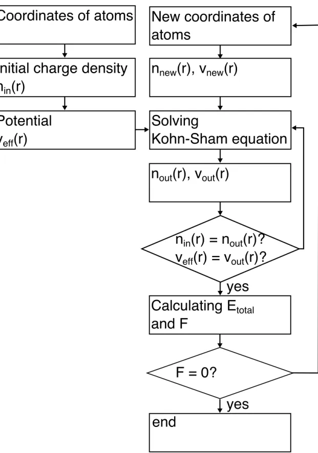
E = N ! j=1 ϵj− 1 2 $ n(r)n(r′) |r − r′| drdr′− $ v(r)n(r)dr + Exc[n(r)] (2.36) In principle, if the exact Exc[n] were used in these equations, the resulting self-consistent density n(r) and energy E would be exact, including all many body effects. Of course, in practical application, one must content oneself with approximations for Exc. Figure 2.1 shows each step to solve the Kohn-Sham equation. The first step is to chose an initial structure of the system and its charge density nin(r). Then, by using the initial charge density, we evaluate the vef f and solve the Kohn-Sham equation. Finally, we generate the nin by a new charge density nout and repeat the same procedure until nin = nout.
2.1.3
Local density approximation
The Hohenberg-Kohn theorem provides some motivation for using approximate methods to describe the exchange-correlation energy as a function of the elec-tron density. The simplest method for describing the exchange-correlation energy of interacting electron systems is to use the local density approximation (LDA). The LDA is widely used in total-energy calculations [21, 22]. In the LDA, the exchange-correlation energy of the electron system is constructed by assuming that the exchange-correlation energy per electron at a point r in the electron gas εxc(r)
is equal to the exchange-correlation energy per electron in a homogeneous electron gas εhom
xc that has the same density as the electron gas at point r. Thus Exc[n(r)] = $ εxc[n(r)]n(r)dr (2.37) and δExc[n(r)] δn(r) = δ[n(r)εxc(r)] δn(r) (2.38) with εxc(r) = εhomxc [n(r)]. (2.39) The LDA assumes that the exchange-correlation energy functional is local.
2.1.4
Generalized gradient approximation
The LDA has been used successfully in solid state physics: The ground state prop-erties of atoms, molecules, and solids agree with these obtained by experiments. In addition, functional forms for the exchange-correlation energy including an ad-ditional information about the electron gas of slowly varying density have been developed. In these functional forms called “generalized gradient approximation (GGA)”, the effects of the charge gradient ∇n(r) are included [23]. The exchange correlation functional Exc[n(r)] of the GGA is with the form
Exc[n(r)] = $
f (n(r),∇n(r))dr (2.40) This semilocal functional has improved results obtained by the LDA: In comparison with the LDA, the GGA tend to improve the total energies, atomization energies, and geometric structure. In this thesis, we use a functional form parameterized by Perdew, Burke, and Ernzerhof (GGA-PBE).
2.1.5
Spin density functional theory
Under the external magnetic field, atoms, molecules, and solids possess Zeeman energy between magnetization densities m(r) depended on external magnetic field and electron spin. The energy of these systems can be written by electron density, n(r), and additional magnetization density m(r). We separate the density n into that of αspin nα(r) and β spin densities nβ(r). By tacking into account of the spin degree of freedom, Kohn-Sham equation is written as
( −12∇2+ vext,σ(r) + $ n(r′) |r − r′|dr′+ δExc[nα, nβ] δnσ(r) )
φiσ(r)≡ ϵiσφiσ(r)(2.41) nσ(r)≡
! i
used by F [nα, nβ] ≡ Ts[nα, nβ] + 1 2 $ $ n(r)n(r) |r − r′| drdr ′E xc[nα, nβ] (2.43) corresponding to Eq.(2.31) where n = nα + nβ. In the DFT including spin degree of freedom, the exchange-correlation energy is written as
ExcLSDA[nα, nβ] = $
d3rnεunifxc (nα, nβ), (2.44) for the LDA and
ExcGGA[nα, nβ] = $
d3rf (nα, nβ,∇nα,∇nβ), (2.45) for GGA.
2.2
Bloch’s theorem
Bloch’s theorem was formulated by Bloch in 1928 to describe wave function of an electron in a periodic potential system. Bloch’s theorem states that the energy eigen-function for the periodic potential system can be written using a periodic eigen-function, unk(r), that has the same periodicity as the potential.
Φnk(r) = eik·runk(r) = unk(r + R) (2.46) where k is the wave vector and R is a lattice vector. The energy eigenvalues εn(k) corresponding to k exhibit periodicity by a reciprocal lattice vector G which is defined as G· R = 2πm for all R, where m is an integer.
ε(k) = εn(k + G) (2.47) Note that all states corresponding to k and any k + G are equal, which means that Φnk(r) is periodic in the reciprocal space, Φk(r) = Φk+G(r). The energies associated with the index n vary continuously with wave vector k and form an energy band identified by the band index n. The eigenvalues for given n are periodic in k, thereby all distinct values of εn(k) occur within the first Brillouin zone of the reciprocal lattice.
2.3
Plane-wave basis set
Bloch’s theorem states that each electronic wave function in the periodic system can be written as the product of a cell-periodic part unk(r) and a wave-like part eik·r. Therefore, the electronic wave functions can be expanded using a discrete plane-wave basis set.
The Kohn-Sham orbitals are expanded by using the plane-wave basis set as follows Ψn(r) = 1 √ Ω ! G Cn,GeiG·r (2.48)
where Ω is the volume of the unit cell. The cell-periodic part of the wave function unk(r) can be expanded using the basis set of a discrete set of plane waves. Therefore, each electronic wave function can be written as a sum of discrete plane waves.
Ψn,k(r) = 1 √ Ω ! G Cn,k(G)ei(k+G)·r (2.49) Plane-wave basis set provides several benefits for DFT calculations. First, plane waves are independent to the positions of the nuclei because they are origin less functions. Therefore, Pulay forces exactly vanish and drastically facilitate force cal-culations. Second, derivatives in real-space are simply multiplications in G-space, and real and reciprocal spaces can be efficiently connected via Fast Fourier Trans-forms. Therefore, one can easily evaluate operators in that space in which they are diagonal. Since plane waves are extended throughout the space, increasing the largest |G| vector in Eq.(2.49), which is called the energy cutoff, Ecut, is the only way in order to improve the quality of calculations.
2.4
Pseudopotential
Physical and chemical properties of atoms, molecules, and solids strongly depends on rearrangements of valence electrons. The core electrons are strongly bound to the nuclei and barely play a role in the chemical bond of materials. On the other hand, DFT calculations with all-electron system by using plane-wave basis set require a tremendous number of plane waves to express the tightly bound core orbitals and to follow the rapid oscillations of the wave functions of the valence electrons in the core region, which needs a vast amount of computational cost. In order to overcome the problem, the pseudopotential method has been proposed [24]. The pseudopotential method decreased the number of plane waves by replacing core electrons and the deep ionic potential with a shallow pseudopotential. In this section, we describe the pseudopotentials used in this thesis.
We introduce the exact solutions of the Schr¨odinger equation for the core electrons by|Ψc >, and those for the valence electrons by |Ψv >.
H|Ψn >= En|Ψn> (2.50) with n = c or v. The valence orbitals can be written as the sum of a smooth function |Ψv > which is called the pseudo wave function, and an oscillating function that is obtained from the orthogonalization of the valence to the core orbitals.
|Ψv >= |φv > + ! c αcv|Ψc > (2.51) where αcv =− < Ψc|φv > . (2.52) The pseudo wave functions |φv > satisfy a Schr¨odinger-like equation with a pseu-dopotential VP P
H|φv >= Ev|φv > + !
c
and then (T + VP P)|φv >= Ev|φv > (2.54) where VP P is defined as VP P = V −! c (Ec − Ev)|Ψc >< Ψc| (2.55) where V is the true potential.
It is almost completely canceled between the large negative potential energy by a valence electron when it is inside the core of an atom, and its large positive kinetic energy which is inherent in the oscillations of its wave function |Ψc >. Therefore, the second term in Eq.(2.55) represents a nonlocal repulsive potential, making the pseudopotential much shallower than the true potential in the core. As a result, the pseudo wave functions |ψV > are smooth and not oscillate in the core region.
2.4.1
Norm-conserving pseudopotentials
Norm-conserving pseudopotentials are constructed by forcing the pseudo wave func-tions to coincide with the true valence wave funcfunc-tions beyond a certain distance while they have the same norm with the true valence wave functions [25]. DFT calcula-tions are generally employed to generate pseudopotentials for a free atom by com-paring with a given reference electron configuration. To construct norm-conserving pseudopotentials, the following four general conditions should be satisfied.
First, the normalized atomic radial pseudo wave function RPD
l with angular mo-mentum l is equal to the normalized radial all-electron wave function RADnl with a principle quantum numbers n and l beyond a cuttoff radius rc.
RPDl (r) = RAEnl (r) (r≥ rc). (2.56) Second, the norm enclosed within rc for the two wave functions should be equal.
$ rc 0 dr|RP Dl (r)|2r2 = $ rc 0 |R AE nl (r)|2r2 (2.57) Third, the valence all-electron and pseudopotential eigenvalues should be equal each other.
ϵP Dl = ϵAEnl (2.58) Fourth, there should not be any nodes in the valence pseudo wave functions gener-ated from the pseudopotential.
2.4.2
Ultrasoft pseudopotential
In the norm-conserving pseudopotential, the all-electron wave function is replaced by a soft nodeless pseudo wave function, which has the same norm as the all-electron wave function within the chosen core radius. For elements with strongly localized
orbitals, the pseudopotentials require a large plane-wave basis set. On the other hand, an ultrasoft pseudopotential, proposed by Vanderbil, provides the pseudo wave function allowed it be as soft as possible within the core region, leading to the signficant reduction of the cutoff energy required [26]. We briefly introduce a procedure to construct the ultrasoft pseudopotential.
All-electron calculations are carried out for a free atom by comparing with the reference configuration to calculate a screened potential vAE(r) and the all-electron wave function|ΨAE i >. (−1 2∇ 2+ vAE− ϵ i)|ΨAEi > = 0 (2.59) where i indicates quantum numbers, i = n, l, m. Then, a pseudo wave function |ψP D
i > and a local potential vAE(r) are constructed, where the pseudo wave function |ΨP D
i >should be smoothly connected at rc.
ΨP Di (r) = ΨAEi (r) (r≥ rc) (2.60) Here, norm-conseravatuin constraint is not imposed. Similarly, a smooth local po-tential, vP D
loc(r), is generated with the constraint that vlocP D matches smoothly to vAE(r) at a cutoff radius r
c
vlocP D(r) = vAE(r) (r ≥ rc) (2.61) Next, orbitals |χi > are calculated to describe the ultrasoft pseudopotential using the pseudo wave function and the local potential.
|χi > = (ϵi+ 1 2∇
2− vP D
loc )|ΨP Di > . (2.62) By defining the matrix of inner products, Bij =< ΨP Di |χi >, we can make a set of orbitals, βi, which is dual to |ΨP Di >,< βi|ΨP Dj >= δij
|βi > = !
j
(B−1)ji|χj > . (2.63) We note that they form the projectors of the nonlocal operators. We further calcu-late the deficit charge density Qij(r) defined as follows.
Qij(r) = Ψ∗AEi (r)ΨAEj (r)− Ψ∗P Di (r)ΨP Dj (r) (2.64) Qij =
$
drQij(r) (2.65)
Qij(r) corresponds to the deficient electron within the cutoff radius rc. Although Qij(r) is zero for the case that the norm is conserved, we now consider to the deficit charge density is not zero. Here, we construct another matrix, Dij, defined as follows. Dij = Bij + ϵjQij. (2.66)
Then,|ΨP D
k > obeys the secular equation. (−1 2∇ 2+ vP D loc + ! ij Dij|βi >< βj|)|ΨP Dk > (2.67) = ϵk(1 + ! ij Qij|βi >< βj|)|ΨP Dk > (2.68) where k is a composite index as in the index i and j. Then, we finally construct the ultrasoft pseudopotential as follows.
ˆ vionP D = vion,locP D (r) +! ij |βi > D(0)ij < βj| (2.69) where vP D ion,loc(r) and D (0)
ij are obtained from following equations,
vion,locP D (r) = vlocP D(r)− vHP D(r)− vxcP D(r) (2.70) D(0)ij = Dij− $ drvP D loc (r)Qij(r) (2.71) where vP D
H (r) and vxcP D(r) are the Hartree and exchange-correlation potentials, re-spectively, calculated from the valence pseudo wave functions. The ultrasoft pseu-dopotential significantly improves the norm-conserving pseupseu-dopotential by relaxing the norm-conservation condition that is usually imposed on the pseudopotential ap-proach. Especially, this method allows first-row and transition-metal elements to be treated efficiently. Ultrasoft pseudopotentails are now adopted quite widely because of significant reduction of the computational cost.
2.5
Effective screening medium method
To inject carriers in surface/interface of materials, we use the effective screening medium (ESM) method developed by Otani and Sugino in 2006 [27]. Their ap-proach consists of solving the generalized Poisson equation under various boundary conditions normal to the surfaces. This task is accomplished with the help of Green’s function technique. The Kohn-Sham equation is solved in a cell with a finite length in the z direction imposing the periodic boundary condition. This treatment is al-lowed when the electrons are not extended much beyond the surface region, but are instead confined within a certain region near the surface of slabs.
By using a slab geometry, which is periodic in the direction parallel to the surface but is not periodic in the perpendicular direction, sandwiched by semi-infinite media, such as vacuum, an electrode, or an electrolyte, we can describe the surfaces and interfaces. We treat the slab part which consists of substrate and adsorbate atoms within DFT. While we treat the medium part using a continuum characterized by relative permittivity ϵ(r) and additional classical charge density nc(r). We assume that the electrons are confined to the region, say z ∈ [−z0, z0], and that the wave functions are solved using the repeated slab of length 2z0, for which standard DFT with plan wave basis set programs are applicable.
The total-energy functional of the ESM model is E[ne, V ] =K[ne] + Exc[ne]− $ drϵ(r) 8π |∇V (r)| 2 + $ dr[ne(r) + nI(r)]V (r) (2.72) where ne(r) denotes the electron charge density, nI(r) is the nuclear charge density, and V (r) is the electrostatic potential. In addition, K and Exc, respectively, rep-resent the kinetic and exchange-correlation energy functional of the electrons; ϵ(r) is the (nonuniform) relative permittivity of the ESM. In this equation, the classical charge density is omitted for simplicity. We also omit the entropic term of the elec-trons. By tacking the variation of the energy, the Kohn-Sham equation is obtained when the total-energy functional is varied by the Kohn-Sham orbital under the or-thonormality constraint. When varied by the electrostatic potential, we obtain a Poisson equation in that the relative permittivity has a spatial dependence. Using a Green′s function for the Poisson equation
∇ · [ϵ(r)∇]G(r, r′) = −4πδ(r − r′). (2.73) Eq.(2.72) could be rewritten
E[ne] =K[ne] + Exc[ne] + 1 2 $ $ drdr′ne(r)G(r, r′)ne(r′) + $ $ drr′ne(r)G(r, r′)nI(r′) + 1 2 $ $ drdr′nI(r)G(r, r′)nI(r′) (2.74)
which has the well-known form for the DFT energy functional, expect that the electrostatic interaction is modified slightly from 1/r to that according to Eq.(2.73). The third, fourth, and fifth terms, respectively, correspond to Hartree energy (EH), electron-ion interaction energy (Ee−i), and ion-ion interaction energy (Eion). The term for interaction between the electrons and the nuclei
$ $
drr′ne(r)G(r, r′)nI(r′), (2.75) can be rewritten for the pseudopotential scheme as
$ $ drdr′ne(r)G(r, r′)ng(r′) + $ drne(r)Vlocshort(r) +! α < φalpha|∆Vps|φα > (2.76) in which the first, second, and third term correspond, respectively, to the long-range local, short-range local, and nonlocal part. In the first term, ng(r) is the effective nucleus charge localized near the nuclear position; Vshort
loc (r) is the short-range local potential; φαs are the Kohn-Sham orbitals; and ∆Vps is the nonlocal part of the
psudopotential, which has a finite range from the nuclear position. We call the sum of the first and second terms the local potential energy (Eloc) hereafter.
This paragraph shows a Green’s function formulation for the solution of the Pois-son equation, which is accomplished by imposing appropriate boundary conditions on Eq.(2.73) and expressing the solution as
V (r) = $
dr′G(r, r′)ntot(r′). (2.77) For this purpose we consider the case in which relative permittivity depends only on z. Then the Poisson equation
∂z[ϵ(z)∂z]− ϵ(z)∇2∥G(r∥− r′∥, z, z′) =−4πδ(z − z′), (2.78) becomes the following in the Laue representation:
∂z[ϵ(z)∂z]− ϵ(z)g2∥G(g∥, z, z′) = −4πδ(z − z′), (2.79) where g∥ is a wave vector parallel to the surface and g∥ indicates the absolute value of g∥. In this thesis, to inject hole/electron by the counter electrode, we use the ESM with the boundary conditions given following.
* V (g∥, z)|z=z1 = 0 ∂zV (g∥, z)|z=−∞= 0 , ϵ(z) = * 1 if |z| ≤ z1 ∞ if |z| ≥ z1 (2.80) In this boundary conditions, the metal electrode is put on only one side of the slab, as z > z1. When the cell is consists of atomic layer materials, the system correspond to the top/back gate field effect transistor in which the metallic continuum that is separately located at z > z1 plays the role of a counter gate electrode.
Coordinates of atoms
Initial charge density
n
in(r)
Potential
v
eff(r)
Solving
Kohn-Sham equation
n
out(r), v
out(r)
n
in(r) = n
out(r)?
v
eff(r) = v
out(r)?
yes
Calculating E
totaland F
F = 0?
yes
end
n
new(r), v
new(r)
New coordinates of
atoms
Chapter 3
Two-Dimensional sp
2
Carbon
Network of Fused Pentagons: All
Carbon Ferromagnetic Sheet
In this chapter, we investigate geometric and electronic structures of a two-dimensional stable carbon allotrope consisting of pentagonal rings.
3.1
Introduction
Pentagons embedded into hexagonal sp2 (threefold-coordinated) carbon networks play a crucial role in determining the geometric and electronic properties of the resulting nanoscale carbon allotropes. By assembling the twelve pentagons with an appropriate number of hexagons, zero-dimensional hollow-cage carbon clusters of nanometer size can be obtained [2, 28]. Fullerenes possess a relatively deep lowest unoccupied state [29] compared with other carbon molecules comprised only of hexagons with a closed-shell electronic structure. Furthermore, they possess a common electronic feature that is characterized by the spherical harmonics Ylm due to their nearly spherical π electron systems [30]. On the other hand, it is known that the detailed electronic structures of fullerene molecules are completely different from each other depending on the symmetry and local atomic arrangement on the nanoscale sphere, even though the molecules have the same size [31, 32].
In the planar hexagonal carbon network, pentagons should appear with the ap-propriate number of polygons. For example, an isolated pentagon embedded in graphene induces the formation of a heptagon adjacent to it to maintain a planar sp2 network, as is found in Stone-Wales-type [33, 34] and fused-pentagon-type [15] topological defects. Since pentagons and other polygons disrupt the AB bipartite symmetry of graphene, such topological defects in graphene occasionally induce an unusual electronic structure at or near EF in addition to the characteristic electronic structure of graphene. Localized states and flat dispersion bands associated with the topological defects are expected to emerge around them [18, 35]. The linearly aligned fused pentagons and octagons effectively terminate the π electron system near EF, and leads to the flat dispersion band at the edges of the topological line
defects [15]. Furthermore, in the case of the topological line defects with the fused pentagons and octagons embedded in CNTs, the nanotubes exhibit ferromagnetic spin ordering along the topological line defects [36].
In general, the defect density strongly affects the physical properties of the host material. Therefore, it is interesting to explore the geometric structure and elec-tronic properties of graphene containing many topological defects. In this chapter, we explore the geometric and electronic structures of a 2D sp2 carbon allotrope con-sisting of pentagons and dodecagons, as a representative structure of the limit of topological defects in sp2 hexagonal networks.
All calculations were performed within the framework of DFT [19, 20] using the Simulation Tool for Atom TEchnology (STATE) package [37]. For calculation of the exchange-correlation energy between electrons, we used the local spin density approximation (LSDA) with a functional form fitted to Monte-Carlo results for a homogeneous electron gas [21, 22]. A Vanderbilt ultrasoft pseudopotential was used to describe the electron-ion interaction [26]. The valence wave functions and charge density were expanded in terms of the plane-wave basis sets with cutoff energies of 25 and 225 Ry, respectively. The structural optimizations were performed until the forces on each atom were less than 5 mRy/˚A for each lattice constant. Integrations in the first Brillouin zone were carried out using 6×6×1 k-points for the isolated sheet consisting of pentagons and dodecagons of C atoms. To investigate the interlayer interaction and the stacking geometries of the sheets, we performed 6×6×6 k-point sampling in the Brillouin zone.
Here, we consider a 2D sp2 carbon sheet consisting of fused pentagon trimers (acepentalene structure [38]) of which three edges are shared by its three adjacent trimers. Accordingly, in the topological view, the network can be regarded as the honeycomb network of fused acepentalenes, which consists of fused pentagonal rings and large dodecagonal pores. With this choice of initial geometry, the resulting material has a honeycomb lattice containing 14 C atoms per unit cell, which forms a 2D covalent network of threefold-coordinated C atoms.
3.2
Energetics and optimized structure
Figure 3.1 shows the total energy per atom as a function of lattice parameter a of the fused pentagon network of threefold-coordinated C atoms. We found that the optimum lattice constant of the 2D fused pentagon network is a = 7.1 ˚A. The calculated total energy is 0.61 eV/atom with respect to the energy of graphene, which is slightly higher than that of the other carbon allotropes containing pentagons and other polygons [39, 40, 41].
At the optimized lattice parameter a, the fused pentagon network retains its planar structure [Figure 3.2], even though an isolated acepentalene molecule has a bowl-shaped conformation. The optimized bond lengths for the acepentalene unit are d1 = 1.40 ˚A, d2 = 1.42 ˚A, and d3 = 1.54 ˚A. The bond lengths are different from those of the isolated acepentalene molecule because of the planar structure of the fused pentagon network. The lengths of the three bonds associated with the vertex of three pentagons (d1) are close to that of the double bond of fullerene, indicating
0.6
0.65
0.7
0.75
0.8
0.85
0.9
6.2
6.4
6.6
6.8
7
7.2
7.4
En
e
rg
y
[e
V
/a
to
m]
Lattice constant [A]
Figure 3.1: Total energy per atom of the fused pentagon network as a function of the lattice parameter a. The energies are measured with respect to the energy of isolated graphene.
d
1d
2d
3 vθ
θ
s(a)
(b)
Figure 3.2: (a) Optimized structure of fused pentagon network in the unit cell. (b) Top and side views of the optimized geometry of the fused pentagon network of sp2 C atoms with a lattice constant of 7.1 ˚A.
the fact that those bonds possess the double bond nature of sp2 C atoms. Indeed, the angles of these bonds are exactly θv = 120◦. In contrast, the bond shared with two acepentalene units (d3) is longer than that of the usual sp2 bond and closer to that of the sp3 bond of diamond. The bond angle associated with the bond is θs = 108◦, which is close to that of sp3 network materials. Furthermore, the bonds at the edges of the dodecagon (d2) also have the sp2 covalent bond nature. The calculated atomic density of the sheet is 0.320 /˚A2, which is slightly less than the atomic density of graphene because of the large dodecagon pores. Therefore, the fused pentagon sheet is light sp2 carbon allotropes with a planar structure.
The kinetic stability of the fused pentagon network is worth investigating. We in-vestigated the geometric structure of the fused pentagon network at temperatures of 200, 400, 600, 800, and 1000 K by performing ab initio molecular dynamics simula-tions for a few picosecond simulation times. The simulasimula-tions showed that the fused pentagon sheet retains its 2D planar covalent network structure at temperatures up to 1000 K. Therefore, once the sheet is synthesized by an appropriate experi-mental method, it is expected to retain its characteristic structure under ambient conditions.
3.3
Electronic strucutre
Figure 3.3 shows the electronic structure of the fused pentagon network with an equilibrium lattice constant of a = 7.1 ˚A. We found that the fused pentagon trimer sheet is a metal with a flat dispersion band that crosses EF. The flat dispersion band has a dispersion of about 0.1 eV around the zone center Γ point. Thus, it is expected that the flat-band state induces spin polarization on the sheet according to EF instability associated with the flat dispersion band. The flat dispersion band splits into lower and upper branches for the majority and minority spin states, respectively, indicating that the sheet exhibits magnetic ordering. The calculated exchange splitting between the branches of the flat dispersion band is about 0.10 eV, and the induced magnetic moment is 0.62 µB/nm2.
Figure 3.4 shows the isosurfaces of the polarized electron spins of the fused pen-tagon network. We found that the polarized electron spins are ferromagnetically aligned and extend throughout the sheet. Therefore, the fused pentagon network is a 2D ferromagnet consisting of only sp2 C atoms whose covalent bonds are fully sat-urated. Furthermore, the extended nature of the spin distribution indicates that the flat dispersion band is not induced by the localized state at certain atomic sites, but is induced by extended π electron states throughout the sheet. The wave function associated with the flat-band state at the Γ point exhibits the extended π electron nature [Figure 3.5(a)], indicating that the delicate balance among the extended π state of C atoms induces the flat dispersion band of the sheet. Furthermore, it should be noted that the spin distribution is similar to the wave function distribution of the electronic state labelled δ at K point [Figure 3.5 (c)]. Similar flat dispersion bands have also been observed in hexagonal network materials with zigzag edges or interfaces [11, 12, 17, 42]. Therefore, the fused pentagon network extends the research field associated with C allotropes with the flat dispersion band.
K
L
M K
β
γ
δ
-6
-5
-4
-3
-2
-1
0
1
2
3
E
n
er
gy
[eV]
Figure 3.3: Electronic energy band of the fused pentagon network near the Fermi level. The solid and dashed lines indicate the majority and minority spin states, respectively. The energies are measured with respect to the Fermi level.
Figure 3.4: Isosurfaces of the spin density, ∆n(r) = nα(r)− nβ(r), of the fused pentagon sheet. The isosurfaces correspond to 0.001 e/au. Gray spheres indicate the atomic positions of the fused pentagon network.
(a) (b) (c)
Figure 3.5: Isosurfaces of the squared wave function of (a) the flat dispersion band indicated by β at the Γ point in Fig. 3.3, (b) the dispersive band just above EF indicated by γ at the K point in Fig. 3.3, and (c) the other dispersive band with higher energy indicated by δ at K point in Fig. 3.3. The isosurfaces correspond to 0.8 e/au. Gray spheres indicate the atomic position of the fused pentagon network. Since the polarized spin has striped distribution along the zigzag direction of the honeycomb network of fused pentagons, the antiparallel spin distribution is expected to occur on this system. To corroborate the issues, we calculate the electronic struc-ture of the sheet with double periodicity normal to the spin strips, which contains two strips of spin density in its unit cell. Under this extended unit cell, we compare the total energy of the ferromagnetic state with that of the antiparallel spin strip state. Our calculation shows that the antiparallel spin configuration between ad-jacent strips emerges as a metastable state in addition to the ferromagnetic state. Calculated total energy of the antiparallel state is higher than that of the ferromag-netic state by 2.6 meV/atom. Therefore, the ferromagferromag-netic spin state is the ground state of the honeycomb network of the fused pentagons.
The fused pentagon network also exhibits another interesting feature in the elec-tronic energy band near EF, in addition to the flat dispersion band. Three states are bunching up together with a small gap of about 0.1 eV at the K point just above the flat dispersion band. Two of the three states possess almost linear dispersion with respect to the wave number, similar to the π and π* states of graphene and graphite. Therefore, the massive Dirac electrons are expected to be located on the fused pentagon network, which does not contain any graphene-like hexagonal cova-lent network structure. The wave functions of these states exhibit a non-bonding nature as in the case of the π state of the graphene and graphite at the Dirac point. The lowest branch of the state is distributed on the atoms adjacent to the vertex of three pentagons [Figure 3.5(b)]. The upper branch is distributed on the atoms at the vertex of three pentagons and the atoms shared by the two acepentalene structures [Figure 3.5(c)]. This suggests that a graphene-like electronic structure is expected to occur in the honeycomb network material with internal geometric structures. However, further analytic investigation is required.
3.4
Stacking structure
The planar materials usually form a stacking structure similar to the case of graphite and transition-metal chalcogenides. Furthermore, because of the bowl shape of the isolated acepentalene molecule, the fused pentagon network sheet is expected to form covalent bonds with adjacent sheets, leading to the three-dimensional network structure. Therefore, we investigated the relative stability and geometric structures of the fused pentagon sp2carbon sheets having stacking structures. By changing the interlayer spacing, we found that the layered system comprising the fused pentagon sheets has an energy minimum at the interlayer spacing of 3.2 ˚A. The calculated energy gain that arises from the interlayer interaction is 20 meV/atom. At the equilibrium interlayer spacing, each fused pentagon sheet still retains its planar structure and does not form covalent bonds with adjacent layers.
3.5
Conclusion
We have investigated the geometric and electronic structures of a 2D sp2 carbon allotrope consisting of pentagons and dodecagons by first-principles total energy calculations based on density functional theory. We found that the 2D sp2 carbon allotrope retains its planar structure at the equilibrium lateral lattice parameter a = 7.1 ˚A. At the equilibrium lattice constant, the calculated total energy of the sheet is 0.66 eV/atom with respect to the energy of graphene, indicating that the structure is energetically stable. Further ab initio molecular dynamics simulations confirmed that the sheet was kinetically stable up to a temperature of 1000 K for simulation times of a few picoseconds. We found that the sheet is a metal with a flat dispersion band that crosses EF. Owing to the flat dispersion band at EF, the state is split into majority and minority spin states, leading to spin polarization on the sheet. The polarized electron spin is ferromagnetically ordered and distributed throughout the whole network of the sheet with a magnetic moment of 0.62 µB/nm2. In addition to the magnetism arising from the flat dispersion band, although the network does not contain any hexagonal rings, the fused pentagon sp2 carbon sheet has a pair of massive Dirac dispersion bands at the K point as in the case of graphene and graphite. Detailed analysis on the wave function indicated that the states possess a non-bonding π electron nature on the honeycomb network of fused pentagons.
Chapter 4
Coexistence of Dirac cones and
Kagome flat bands in a porous
graphene
In this chapter, we investigate the geometric and electronic structures of porous graphene networks consisting of phenalenyl and phenyl groups, which are connected alternately with C3 symmetry via single bonds to form a honeycomb network.
4.1
Introduction
Polymerization and oligomerization of hydrocarbon molecules can provide struc-turally well-defined π electron networks with various dimensionalities. These low-dimensional or porous graphene networks have attracted much attention because of their high surface areas and electronic structure modulation, which are promising for application in energy and electronic devices in the near future [43, 44, 45, 46]. The electronic structures of such polymers and oligomers strongly depend on the combination of hydrocarbon molecules and polymer chains, which allows us to tai-lor their physical and chemical properties by fabrication under optimum external conditions [47, 48, 49, 50]. This indicates that porous magnetic C nanomateri-als may be synthesized by polymerizing hydrocarbon molecules with radical spins. Phenalenyl is one possible candidate as a constituent unit of such magnetic ma-terials [51, 52, 53, 54, 55]. Dimerization of triphenylphenalenyl and cyclodehydro-genated phenalenyl leads to complexes containing two phenalenyls possessing singlet and triplet spin coupling as their stable states [56, 57, 58, 59]. Despite intensive ex-perimental and theoretical works on two phenalenyls connected via a covalent π network, the possible electronic structures of 2D networks consisting of phenalenyl molecules have not yet been investigated in detail. The three-fold symmetry of the phenalenyl network causes honeycomb networks of radical spins or non-bonding state to be distributed on phenalenyls with appropriate interconnect units, leading to interesting electron systems.
All calculations were performed within the framework of DFT [19, 20] using the STATE code [37]. To calculate the exchange-correlation energy among interacting
electrons, we used the GGA with the Perdew-Burke-Ernzerhof functional [23]. To investigate the spin-polarized states of the porous hydrocarbon sheets, the spin de-gree of freedom was taken into account for all calculations. Vanderbilt ultrasoft pseudopotentials were used to describe the electron-ion interaction [26]. The va-lence wave functions and charge density were expanded in terms of the plane waves with cutoff energies of 25 and 225 Ry, respectively, which sufficiently describe the electronic structure and energetics of hydrocarbon molecules and graphene-related materials [60]. To simulate an isolated porous hydrocarbon sheet, the sheet was separated by a vacuum spacing of 10.58 ˚A. Atomic structures of the sheets were optimized until the force acting on each atom was less than 1.33×10⁻³ HR/au. Integration over the Brillouin zone was carried out using an equidistance mesh of 2×2×1 k points. To inject holes into the sheet, we used the ESM method to solve the Poisson equation under the field-effect-transistor structure with a counter gate electrode situated above the sheet with vacuum regions of 5.29 ˚A [27].
4.2
Energetics and optimized structures
Figure 4.1 shows the optimized structures of 2D porous hydrocarbon networks con-sisting of phenalenyl connected via phenyl with various arrangements under the hexagonal cell parameter of 19.4 ˚A. For all phenyl arrangements, the phenalenyl units retained a planar structure as their stable conformation. As illustrated in Fig. 4.1(a), two phenalenyl units per unit cell form a hexagonal lattice in which phenyl units connect adjacent phenalenyl units through covalent bonds like those of graphene. Simultaneously, three phenyl units form a Kagome lattice in which phenalenyl acts as an interunit bond. Because of the planar conformations of both phenyl and phenalenyl, the porous hydrocarbon sheet possesses a 2D π electron system. Rotation of phenyl modulates the π electron system: By rotating one of three phenyl units, the π electrons form a chain network in which the alternating phenalenyl and phenyl units form zigzag chains (chain structure in Fig. 4.1(b)). By rotating two phenyl units, π electrons are segmented into a phenalenyl dimer contain-ing a phenyl unit (dimer structure in Fig. 4.1(c)). Finally, π electrons are localized on each phenalenyl and phenyl in the monomer structure depicted in Fig. 4.1(d).
The total energies of the porous hydrocarbon sheets with various phenyl confor-mations are listed in Table 4.1. Among the four structures, the planar structure is the least stable with a total energy higher by 0.8 eV per cell (16 meV/ C atom) than that of the ground state conformation. The total energy monotonically decreases by increasing the number of rotated phenyl units, although the π conjugation de-creases. The decrease of the total energy with respect to the rotation of phenyl units is caused by the steric hindrance between hydrogen atoms attached to the phenyl and phenalenyl. Since the hydrogen atoms attached to the phenyl and phenalenyl are positively charged, the hydrogen atoms tend to separate each other to reduce the Coulomb’s repulsive interaction. The thermal stability of the porous hydrocarbon sheets was investigated by ab initio molecular dynamics simulations conducted at a constant temperature up to 3000 K for simulation times of 1 ps. Under all temper-atures, all structures retained their initial network topologies. On the other hand,
(a) (b)
(c) (d)
Figure 4.1: Optimized structures of porous hydrocarbon sheets consisting of phenalenyl and phenyl groups with (a) planar, (b) chain, (c) dimer, and (d) monomer conformation. Black and pink balls denote carbon and hydrogen atoms, respec-tively. Black dotted lines show the unit cell of each network. Blue hexagons and red triangles show hexagonal and Kagome networks of phenalenyl and phenyl units, respectively.
Table 4.1: Relative total energies of porous hydrocarbon sheets consisting of phenalenyl and phenyl groups with antiferromagnetic (AF), ferromagnetic (F), and non-magnetic (NM) states. The energies are measured from that with the planar conformation without spin polarization.
Structures AF state [meV] F state [meV] NM [meV]
2D 803 817 1116
Chain 301 310 612
Dimer 159 163 471
Monomer 0 0 313
at the elevated temperatures, the phenyl units are tilted by angles of 20-40 degrees from the planar arrangement owing to the steric hindrance between hydrogen atoms attached to the phenalenyl and phenyl. Thus, we confirm that the 2D networks of phenalenyl and phenyl proposed here are both statically and dynamically stable and are expected to be stable under ambient conditions once they are synthesized experimentally.
4.3
Electronic structures
Figure 4.2 presents the electronic structures of 2D porous hydrocarbon sheets con-sisting of phenalenyl and phenyl. The planar structure possesses a characteristic feature around EF [Figure 4.2(a)]. The porous hydrocarbon sheet is a zero-gap semiconductor with a pair of linear dispersion bands at EF. In addition to the lin-ear dispersion bands, we find three bunched states just above and below the linlin-ear dispersion bands. One of the three branches exhibits perfect flat band nature while the remaining two have finite band dispersion, consistent with their Kagome band structure. These observations indicate that Dirac cone and Kagome flat bands coex-ist in the porous hydrocarbon sheet of phenalenyl and phenyl with flat conformation. The Dirac cone is robust while the Kagome bands are fragile against the rotation of phenyl: A Dirac cone is observed for all porous hydrocarbon sheets, regardless of the phenyl conformation. In contrast, the Kagome flat bands are absent for the sheets with chain and dimer structures, because the electron system of the phenyl unit does not retain the symmetry of the Kagome lattice.
We evaluated tight-binding parameters of the Dirac cone and Kagome band in the different sheet conformations from their bandwidth. The calculated transfer in-tegrals of the Dirac cone tD are 17, 16, 14, and 10 meV for the planar, chain, dimer, and monomer conformations, respectively. Because of the narrow bandwidth, the Fermi velocities of the Dirac cone are 1.2×10⁴, 1.4×10⁴, 0.5×10⁴, and 1.6×10⁴ m/s for the planar, chain, dimer, and monomer conformations, respectively. Therefore, the porous hydrocarbon sheets are possible fields for strongly correlated electron systems that exhibit peculiar physical phenomena. A low Fermi velocity may cause large Fermi level instability even though the sheets possess zero density of states at EF. For the Kagome bands, we also evaluated the transfer integral tK. The
calcu--3 -2 -1 0 1 2 3 Energy [eV]
(a)
K
L
M K
(b)
-3 -2 -1 0 1 2 3 Energy [eV]K
L
M K
-3 -2 -1 0 1 2 3 Energy [eV](c)
K
L
M K
(d)
-3 -2 -1 0 1 2 3 Energy [eV]K
L
M K
Figure 4.2: Electronic structures of porous hydrocarbon sheets consisting of phenalenyl and phenyl groups with (a) planar, (b) chain, (c) dimer, and (d) monomer conformation. Energies are measured from that of the Fermi level.
(a) (b)
(c) (d)
Figure 4.3: Isosurfaces of the wave function of the Dirac cone of porous hydrocarbon sheets consisting of phenalenyl and phenyl groups with (a) planar, (b) chain, (c) dimer, and (d) monomer conformation at the K point.
lated tKare 27 and 21 meV for the planar and monomer conformations, respectively. To clarify the physical origin of the Dirac cone in the planar system, we investi-gated the squared wave functions of the states at the K point [Figure 4.3(a)]. The wave functions are localized on phenalenyl units even though this porous hydro-carbon sheet possesses a 2D planar π electron network. By focusing on the wave function distribution within each phenalenyl, the state exhibits non-bonding nature in each phenalenyl unit. This indicates that the electron states associated with the Dirac cone can be ascribed to the singly occupied states of isolated phenalenyl monomers. In addition to the non-bonding nature within each phenalenyl unit, the wave function also exhibits non-bonding nature between adjacent phenalenyl units. Thus, the pair of linear dispersion bands at EF is ascribed to the hexag-onally arranged singly occupied state or a radical spin state of phenalenyl unit. Similar non-bonding nature within and between phenalenyl units was also found for the porous hydrocarbon sheets with chain, dimer, and monomer conformations [Figures 4.3(b)-4.3(d)].
Next, we examined the wave function associated with the Kagome band. Fig-ure 4.4 shows the isosurfaces of the squared wave functions of the Kagome bands just below EF at the Γ point. For the planar conformation, the wave functions are mainly distributed on the phenyl unit with the character of the HO states of phenyl molecules and are extended throughout the networks. Therefore, the flat disper-sion band is ascribed to the delicate balance of the electron transfer among the HO state of the three phenyl units of the Kagome network, as in the case of the usual

![Figure 1.3: Electronic structures of graphite [1]. The energy is measured from that of the Fermi level.](https://thumb-ap.123doks.com/thumbv2/123deta/8498998.922962/13.892.128.752.161.427/figure-electronic-structures-graphite-energy-measured-fermi-level.webp)
![Figure 1.6: Geometric structures of graphene nanoribbon with edge angles of (a) 0 ◦ (armchair edge), (b) 8 ◦ , (c) 16 ◦ , (d) 23 ◦ , and (e) 30 ◦ (zigzag edge) [9].](https://thumb-ap.123doks.com/thumbv2/123deta/8498998.922962/16.892.139.754.144.1101/figure-geometric-structures-graphene-nanoribbon-angles-armchair-zigzag.webp)
![Figure 1.9: (a) Geometric and (b) electronic structures of graphene with topological line defect consisting of pentagonal and octagonal rings [15]](https://thumb-ap.123doks.com/thumbv2/123deta/8498998.922962/19.892.230.731.432.804/geometric-electronic-structures-graphene-topological-consisting-pentagonal-octagonal.webp)
![Figure 1.10: Scanning electron microscope images of graphene with grain bound- bound-ary [16].](https://thumb-ap.123doks.com/thumbv2/123deta/8498998.922962/20.892.118.761.382.861/figure-scanning-electron-microscope-images-graphene-grain-bound.webp)
![Figure 1.11: Contour plots of spin densities of heterosheet consisting of graphene and h-BN [17]](https://thumb-ap.123doks.com/thumbv2/123deta/8498998.922962/21.892.136.747.182.595/figure-contour-plots-spin-densities-heterosheet-consisting-graphene.webp)