西 南 交 通 大 学 学 报
第 54 卷 第 4 期2019 年 8 月
JOURNAL OF SOUTHWEST JIAOTONG UNIVERSITY
Vol. 54 No. 4 Aug. 2019
ISSN -0258-2724 DOI:10.35741/issn.0258-2724.54.4.26 Research article
Electrical and Electronic Engineering
O
PTIMUM
D
ESIGN OF
I
NTEGRATED
S
WITCHED
C
APACITOR
C
IRCUITS
U
SING
0.5-
µM
CMOS
T
ECHNOLOGY
基於 0.5μm 互補金屬氧化物半導體技術的集成開關電容器電路的優化設計
Ahmed S. Al-Jawadi, Mohammed A. Al-Shorbaji, Shamil H. Hussein, Dr. Khalid K.
Department of Electrical Engineering, University of Mosul, Mosul, Iraq
Shamil_alnajjar84@uomosul.edu.iq
Abstract
Analytical optimization is used to create an optimized design of integrated switched-capacitor charge pump (CP) circuits. In integrated circuits design, voltage gain, output resistance, output ripple voltage, conversion efficiency, and capacitor sizing based on area constraints and power consumption are required for manufacturing. In this paper, an analytical optimization is performed and applied to conventional and bootstrapped techniques for fifth stages switched-capacitor charge pump circuits in order to optimize the parameter values. These circuits result in the appropriate function formulations that result in low power, minimum charge, and minimal area of the silicon chip. This paper describes an optimization method based on the improvement of these parameters that requires a trade-off between the above variables of the bootstrapped technique. The simulated circuits are designed in 0.5-µm complementary metal oxide semiconductor (CMOS) technology with 2 V devices. All of the integrated switched-capacitor circuits were designed with the same specification, which include 10 pF stage capacitance, 2 V supply voltage, clock frequency of 50 MHz and identical sizes of charge transfer switches (transistors). The bootstrapped technique that was implemented for all of the CPs' circuits has good efficiency of about (68.5 %), compared with (53 %) for conventional CPs' circuits.
Keywords: Conventional and Bootstrapped Switched-Capacitor Circuit, Pumping Capacitance, Silicon Chip Area
and Power Dissipation.
摘要 分析优化用于创建集成开关电容器电荷泵(CP)电路的优化设计。在集成电路设计中,制造需要基于面 积限制和功耗的电压增益,输出电阻,输出纹波电压,转换效率和电容器尺寸。在本文中,对第五级开关电 容器电荷泵电路进行了分析优化,并将其应用于常规和自举技术,以优化参数值。这些电路产生适当的功能 公式,从而导致低功耗,最小电荷和最小硅芯片面积。本文介绍了一种基于这些参数改进的优化方法,该方 法需要在自举技术的上述变量之间进行权衡。仿真电路采用 0.5 微米互補金屬氧化物半導體 技术和 2 伏器 件设计。所有集成开关电容器电路的设计均具有相同的规格,包括 10 的的级电容,2 伏的电源电压,50 兆赫 的时钟频率以及相同尺寸的电荷转移开关(晶体管)。与所有 CP 电路的(53 %)相比,为所有 CP 电路实 施的自举技术的效率约为(68.5 %)。 关键词: 常规和自举式开关电容器电路,泵浦电容,硅芯片面积和功耗。
I.
I
NTRODUCTIONThe input supply voltage (VDD) is converted to
higher or lower Direct Current (DC) output voltage (VO) by using switch-capacitor CP circuits.
Charge pumps contain only the capacitors and transistors required to produce the constant DC voltage for implementation [1]. The Dickson charge pumps (DCP) are the simplest type of switched capacitor circuit and are very popular. These circuits are used on one chip with other multiple compounds of an integrated system. The voltage gain (AV) of the DCPs is increased
proportional to the increase in the number of circuit stages (N) and vice versa [2].
The switched-capacitor circuits eliminate the voltage drop at the output switches, reduce the output voltage ripple, and use only two non-overlapping phases (V1 and V2). Moreover, the
voltage across each transistor is never higher than the power supply voltage VDD. It presents unique
design challenges in terms of power efficiency, device reliability, driving capability, and performance. At high output currents, the overdrive voltage decreases, causing the output resistance to rise due to higher switch resistance, thus increasing resistive power losses, reducing power conversion efficiency and driving capability. The increasing power conversion efficiency of the CP circuits is not only seen in battery-powered systems, but also in many applications with common supply voltages, which reduce the integrated circuits packaging cost through heat dissipation. The large extension of the load currents (Io) and output voltages (Vo) of CPs are desirable because of the driving capability feature. However, the minimization of the chip area and steady-state operating points are important to the design. The reliability of MOS structures is another feature that is important to be solved by the three menacing mechanisms called the punch-through, oxide breakdown, and well-diffusion junction breakdown of metal oxide semiconductor field effect transistor MOSFET [3].
P. Modi [4] mainly deals with the innovation and design of the charge pump circuit. The charge pump circuit is controlled by a non-overlapping clock phase system that allows for a more complex design. The strength of the loading current of the proposed circuit design in this paper is about 45mA, which results in high power consumption with a need for a wide range of input voltage from 3V to 7V with a power conversion efficiency of 90%. Conventional charge pump 0.5-μm CMOS process technology is used in this system but the power losses and leakage of current are high.
In [5] C.P. Hsu and H. Lin, they explain two models of the charge pump circuits: four stage voltage and P-channel MOS CPs. The dynamic charge transfer waveforms and charge balance methods are used to enhance the output voltage and power efficiency, but they provide or generate more output current and increase the size of the transistors. Voltage doubler circuits have NMOS, PMOS transistors with threshold voltages of 0.44 V, −0.495 V. P-channel MOS (PMOS) charge pump 0.18-μm CMOS process technology is used in this system but the input voltage is high at about VDD = 1.8 V, and the pumping capacitance
is C = 5 pF while the clock frequency is 10 MHz. This analysis found an optimum point based on the minimization method for the number of stages of the switched-capacitor CPs, the area of the chip, and the capacitor sizing of integrated CP. OrCad Cadence software is used to design and analyze switched-capacitor charge pump circuits, utilizing bootstrapped techniques that achieve high performance like increased power conversion efficiency, output voltages, power gain, and reduction of the dynamic power losses and ripple output voltages. 0.5-μm CMOS process, 2 V supply voltage, C = 10 pF, f = 50 MHz or greater and Io = 500 mA are used in this system. The results achieved are very good and can be used on wide band frequencies from 25 to 100 MHz for switched-capacitors in comparison to conventional charge pump voltage multiplier circuits.
II.
M
ODEL OFC
HARGEP
UMPThe number of stage circuits, chip area occupation and current dissipation are very important design parameters for switched– capacitor CPs. Moreover, purely capacitive load, rise time, and the charge consumption during the rise time are important to the design. However, the clock frequency that is applied to the circuits is represented in the design parameter. It is set to the value of the clock found inside the system [6].
The stages of the CPs are connected to the required voltage Vo of the switched-capacitor circuits with pure capacitive load. This can be simplified into [6]:
𝑉𝑜 = 1 + 𝑁 VDD −
𝑁𝐼𝑂
𝑓 ∗ 𝐶 (1) The physical aspects of CPs, such as the total silicon chip area (ATot), may be neglected. Based
on the size of the capacitors, the area is found, the approximate (ATot), simply using the relative area,
3 ATot = k ∗ N2 1 + N . VDD − Vo ∗ Io f (2)
The (k) is suspended in the process that optimizes the capacitors. N is the stage of the circuit design, Vo is output voltage, and Io is the load current.
The current consumption (IDD) can be
formation by two contributions [7]. The ideal CPs behavior is called drain current (IID), and another
term named parasitic effects (IPar). The current
consumption is given as:
𝐼𝐷𝐷 = 𝐼𝐼𝐷 + 𝐼𝑃𝑎𝑟 (3)
where IID is the drain current that flow to the
load and generated by the input supply. It is transferred in each period from one capacitor to another. Also, IPar is the mainly charge and
discharge current in every time periodic (T) of the total parasitic capacitor. The current dissipation in the steady state is presented by equation (4) [6]: IDD = 1 + N + 𝛼 . N 2 1 + N . 𝑉𝐷𝐷 − Vo . 𝑉𝐷𝐷 . Io (4)
The current and the power consumption are independent from the clock frequency and the total CPs capacitance, but they are linearly proportional to the current load Io [8][11].
Another useful design parameter of the switched capacitor CP circuit is charge consumption, which is evaluated by depending on the purely capacitive load. It is delivered by the supply VDD to the CPs during rise time, and it can
be divided into three main contributions: 𝑄𝑇
= 𝑄𝐿+ 𝑄𝑃𝑎𝑟
+ 𝑄𝑃𝑢𝑚𝑝 (5)
where QT is the total charge consumption,
QL is the charge to the load, QPump is the charge
during the transient of the pump capacitors, and QPar is the contribution dissipated in the parasitic
capacitance. Substitute each, giving in Eq. (5) the total charge consumption, which has been drowned by the rise time of the input supply voltage [6]: QT(𝑡𝑟) = 1 + N 𝑣𝑥− 𝑣𝑥0 + 𝛼N2lnN + 1 − 𝑣𝑥0 N + 1 − 𝑣𝑥 (𝐶𝐸𝑞 + 𝐶𝐿). 𝑉𝐷𝐷 (6)
where CEq is the capacitance, which is equal to
the total pumping capacitance divided by 3, and vx and vx0 are equal to the ratio between the
voltage Vo and the supply voltage VDD of the CPs
circuits at the rising time (tr). These voltages are given as follows [6]: 𝑣𝑥 = 𝑉𝑜(𝑡𝑟) 𝑉𝐷𝐷 𝑎𝑛𝑑 𝑣𝑥0= 𝑉𝑜(0) 𝑉𝐷𝐷 (7)
III. D
ESIGNS
TRATEGIES OFC
HARGEP
UMPC
IRCUITSThe start of the design strategy is the stage N of the switched-capacitor CPs circuits with a certain value of the load current Io that represents one of the important parameter designs. To evaluate the optimum N of the proposed design, two strategies that can be used are the silicon chip area minimization and the power or current consumption. The specification design includes VDD = 2 V, Vo = 8 V, C = 10 pF, f = 50 MHz, α =
0.15, and Io = 500 µA.
A. Optimum Value of Area
The optimum value of stage N was evaluated at the chip area minimization. The derivative of Eq. (2) is mentioned above with respect to N and sets the result derivative to zero to find optimum N. On the other hand, the derivative of the current Io is evaluated from Eq. (1) with respect to N and set to zero in order to get the maximum value of the current provided to the load of the design circuit [9]. After solving for N, the optimum value of the number of stages (NAopt) was calculated,
given as: 𝑁𝐴𝑜𝑝 楲= 2 . 𝑉敤 𝑉𝐷𝐷 − 1 (8) The pumping capacitance (C) can be calculated from Eq. (4), given as:
C = 𝑁 ∗ 1
1 + 𝑁 . VDD− Vo
∗ Io
f (9) Substituted the optimum value NAopt in the Eq.
б
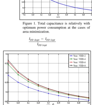
Figure 1. Total capacitance is relatively with optimum power consumption at the cases of area minimization. 0.1 0.15 0.2 0.25 0.3 0.35 0.4 0.45 0.5 0.05 0.1 0.15 0.2 0.25 0.3 0.35 0.4 0.45 ALFA Area Minimization 𝐶𝑇 𝐼𝑜𝑝𝑡− 𝐶𝑇 𝐴𝑜𝑝𝑡 𝐶𝑇 𝐴𝑜𝑝𝑡
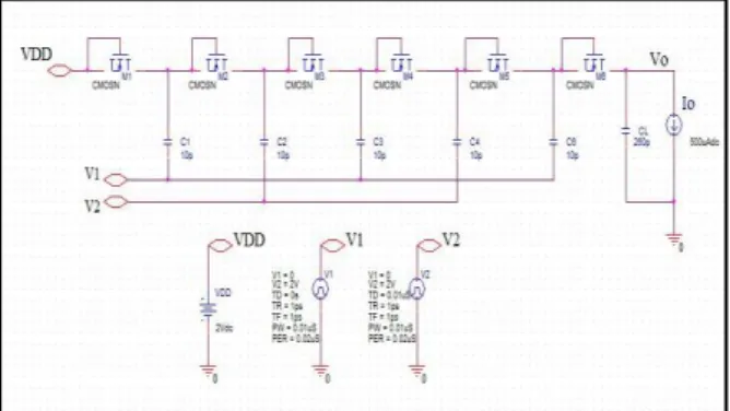
Figure 2. Current consumption is relatively with area minimization at the case of optimum current consumption. б 0.1 0.15 0.2 0.25 0.3 0.35 0.4 0.45 0.5 0.05 0.1 0.15 0.2 0.25 0.3 ALFA Vout / VDD=2 Vout / VDD=4 Vout / VDD=6 Vout / VDD=8
capacitance based on total chip area minimization [9]. 𝐶𝑇 𝐴𝑜𝑝𝑡 = 𝑁𝐴𝑜𝑝𝑡 ∗ 1 1 + 𝑁𝐴𝑜𝑝𝑡 . VDD − Vo ∗ Io f (10) where CT Aopt is the optimum value of the CP
capacitance at implemented chip area minimization and NAopt is the optimum number of
stages of CP circuits.
B. Minimum Value of Power Consumption
The optimum value of stages N of the design was calculated at minimum current consumption. It is obtained by setting the derivative of Eq. (3) to zero, as shown above in regard to N. After solving for N, the optimum value of number of stages (NIopt) has been calculated, given as:
𝑁𝐼𝑜𝑝𝑡 = 1 + 𝛼 1 + 𝛼 . 𝑉𝑜 𝑉𝐷𝐷 − 1 (11) Finally, the optimum value of N that has been obtained from Eq. (8) is substituted into Eq. (10), the pumping capacitance (C) that is required for the optimized design at implemented current minimization [6]. 〱𝑇 𝐼𝑜𝑝𝑡 = 𝑁𝐼𝑜𝑝𝑡 ∗ 1 1 + 𝑁𝐼𝑜𝑝𝑡 . VDD− Vo ∗ Io f (12) C. Comparison of Design Strategies
To compare the two considered design strategies above, first start by evaluating the increase in chip area when the power consumption design is minimum, then compare it to the minimum value of the area design [8].
The value of the NAopt and NIopt have been
calculated from Eq. (8) and Eq. (11), then the total CP capacitance was obtained at the optimum value of N for silicon chip area and current consumption, respectively. Figure 1 as shown below explains the increment of the optimum capacitance that is relative to the optimization of power consumption at the minimum value of the area. It can be seen from this figure that the function of α has decreased and is about equal to 0.4 and 0.2. The silicon area of the design has increased by about 40% at α equal to 0.1 and 20%
at α equal to 0.2. When α is much lower than 0.1, it is does not occur and is not plotted in this figure.
The current increase of the power consumption at the minimum chip area design. Substituting Eq. (7) or (10) in Eq. (4) to calculate IDD. Figure 2
shows the final term of IDD is obtained at the
minimum value for both the area and current design strategy with different value for Vout / VDD.
𝐼𝐷𝐷 𝐴𝑜𝑝𝑡 − 𝐼𝐷𝐷 𝐼𝑜𝑝𝑡
𝐼𝐷𝐷 𝐼𝑜𝑝𝑡
It can be seen from Figure 2 that the current consumption IDD is a function of α and the ratio
(Vo/VDD). The optimum value of current
dissipation increases with a decreasing function of constant α and an increasing function of the ratio. For the optimum area, the current consumption increased, but not higher than 20% and Vo/VDD is
higher than 4. On the other hand, the current consumption increased by about 20% higher, provided that α is lower than 0.15 [6].
Analytical optimization is used to minimize of both the chip area and power consumption that mainly affect the number of stage Ns and other performances of the CP circuit design. Figure 3 shows the optimum values of the silicon chip area and current consumption at different values of N. From this figure, the optimum value of the number of stage Ns is 5 with required constraint
5
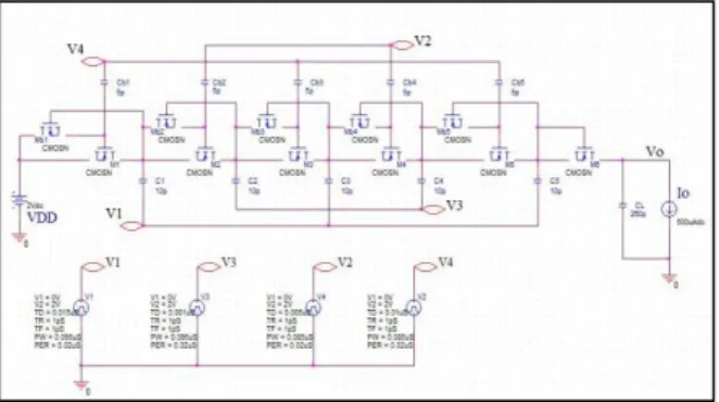
Figure 4. Conventional switched – capacitor charge pump circuit.
parameter designs such as area chip minimization and power consumption minimization.
IV.
S
WITCHED–
C
APACITORCP
S Switched–Capacitor CPs circuits is used in the modern optimum circuit systems like embedded nonvolatile memories. Dickson CPs is the most popular CPs circuits which consisting the charge transfer diodes and charge pumping capacitance as shown below in Figure 4. Non-overlapping clock signals V1 and V2 are anti-phased with anamplitude of supply input VDD. The charge and
discharge processes on the pumping capacitors of the circuits has been controlled by clock pulses. The output voltage Vo of the DCPs circuit is increased through pumps charge from the input supply voltage to the output terminal stage by stage. The realization of the charge transfer diodes using Pass transistors NMOS. However, the voltage loss of these diodes is undergo because of the threshold voltage and body effect of the charge transfer. So the efficiency of the single switched–capacitor CPs is very small little at lower input supply voltage. The ripple output voltage of the single switched–capacitor circuits is given in Eq. (12) [6].
𝑉𝑟 =
𝐼𝑜
𝑓 ∗ 𝐶𝐿
(13) where Vr is the ripple voltage of output circuit,
I_o is the current, CL is the capacitance of the load
circuit, and f is clock pulse of input frequency. The voltage gain, output resistance, and conversion efficiency of integrated charge pump circuits is evaluated by using analysis method. The development of an optimization method is used to improve the response of the required constraints via the sizing of the pumps capacitance that based on area minimization. The structure of charge pump circuits are optimized and compared with other circuits to reduce the losses due to devices parasitic. The
switched-capacitor CPs is the best structure for integration chip. Bootstrapping technique is implemented to the conventional the switched-capacitor charge pump. It is used to improve performance and conversion efficiency of proposed circuit design [6].
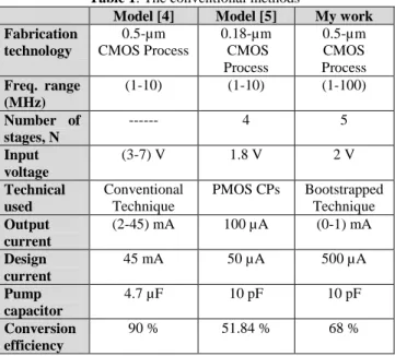
In the bootstrapped switched–capacitor CPs [6]. Four Non-overlapping clock phases (V1, V2, V3
and V4) is alleviated from drop of the switch
voltage, varying on resistance of the charge transfer, and low conduction of the circuit. Bootstrapping technique is used to prevent the short circuit current from nodes at higher voltages to nodes at lower voltages as shown below in Figure 5. The configuration of the bootstrapped circuits is needed to generation of four appropriate clock pulses and pass MOS transistors. These circuit include the sizing of the boosting capacitance (Cb) equivalent to bootstrap the gate
of the pass transistors. The gate voltage of the pass transistor is reduced because the capacitance in the load terminate (CL) is low. The voltage
swing to the gate of the pass transistor and other parasitic capacitances is sufficient through added the capacitor (Cb). The boosted voltage is given by
[6]:
𝑉𝑑𝑑 = 1 + 𝑉𝐷𝐷∗
𝐶𝑏
𝐶𝑏+ 𝐶𝐿
(14) The turn-on resistance of the charge transfer transistors of an N-stage switched-capacitor CPs is assumed of zero in order to determine output voltage Vo. The transfer capacitors of each stage are alternately charged to the voltage of the previous stage and then boosted by VDD to charge
the next stage. The voltage in the output terminate depends on the number of stages and input voltage, then it is expressed by Eq. (15) [6].
𝑉𝑜 = 1 + 𝑁 𝑉𝐷𝐷 (15)
Figure 3. Normalized value of the minimum current and area consumption versus with number of stages N.
2 4 6 8 10 12 14 16 0 1 2 3 4 5 6 7 8 Number Of Stages (N) Area Minimization Power Minimization 𝑰𝑫𝑫 𝑰𝑫汜 𝑴𝒊𝒏 𝑨𝑻𝒐𝒕 𝑨𝑻𝒐𝒕 𝑴𝒊𝒏 𝑽𝑫𝑫= 𝟐𝑽 𝒇 = 𝟓𝟎𝑴𝑯𝒛, 𝑽𝒐= 𝟖𝑽, 𝑰𝒐= 𝟓𝟎𝟎м𝑨 𝒂𝒏𝒅 б = 𝟎. 𝟏𝟓
Figure 5. Bootstrapped switched – capacitor charge pump circuit. 0 0.1 0.2 0.3 0.4 0.5 0.6 0.7 0.8 0.9 1 x 10⁻³ 2 3 4 5 6 7 8 9 10 11 12
Output current (Io)
O ut put V ol ta ge ( V ol t) Conventional Switch-Capacitor CP Bootstrapped Switch-Capacitor CP
Figure 6. The relative between loading current and output voltage for switched – capacitor CPs circuit at N=5, C = 10 pF, f = 50 MHz, and VDD = 2 V. 0 0.1 0.2 0.3 0.4 0.5 0.6 0.7 0.8 0.9 1 x 10⁻³ 0 1 2 3 4 5 6
Output Current (Io)
O ut put P ow e r (m W a tt ) Conventional Switch-Capacitor CPs Bootstrapped Switch-Capacitor CPs
Figure 7. The relative between output power variation and load current for conventional and bootstrapped of switched–capacitor CP at N = 5, C = 10 pF, f=50 MHz, and VDD = 2 V.
where C, CL are the pumping and load
capacitance respectively. VDD is the supply
voltage, Io is the load currents, and f is the clock pulse of the input frequency.
V.
O
RC
ADC
ADENCES
IMULATIONR
ESULTSThe realization and simulation of switched-capacitor charge pump circuits is done by using an OrCAD PSpice simulator under the studied setting of Io = 500 μA, stage capacitance (C = 10 pf), input supply voltage (VDD = 2 V), input clock
frequency (f = 50 MHz), number of stages (N = 5), and identical device dimensions. Analytical optimization has been implemented in a MATLAB software to certify the operation of CP circuits under the resultant optimum parameter values. The output voltage, ripple output, rising time, and efficiency satisfy the desired requirements for the CPs through optimum design parameters resulting from an optimization methodology [6]. Figure 6 below shows details of the simulation of the relationship between the output voltages of the CP circuits and load currents Io. When the output current is increased, the voltage is decreased.
Simulation results show that the bootstrapped switched-capacitor charge pump provides an open-circuit output voltage of 8.89 V, compared with a voltage of 7 V provided by the conventional switched-capacitor charge pump at Io = 500 µA because short-circuit losses are prevented and parasitic capacitances of the pass transistors do not increase the value of β at the voltage multiplier internal nodes in the bootstrapped technique. The simulated output resistance is nearly constant (RO = 10.18 KΩ),
while the output resistance of a conventional CP increases significantly. The output power of the conventional and bootstrapped switched-capacitor CP circuits have been simulated and changing relative to changes in the load current at a
pumping capacitance of 10 pF and f = 50 MHz. The relationship between output power and current Io is shown in Figure 7 [10].
The output voltages Vo of the proposed conventional and bootstrapped CPs is proportional to the input supply voltage VDD. When the VDD is
increased, the voltage Vo is increased. Figure 8 shows the simulated output result of CPs circuits at load capacitive CL=260pF and load current
Io=500µA under different power supply input voltages. Also the CPs circuits are simulated at different clock frequencies. Figure 9 explains that the increase of the input clock pulse frequencies lead to increase in the output voltages for the CPs circuits. However, the proposed bootstrapped CPs have higher output voltages under the same conditions, such as input supply voltage and load current [6].
Output power of these CPs circuits is proportional to the input power supply voltages; when the input supply voltage is increased, the power outputs will be increased. Figure 10 as shown below presents a simulation of this relationship between power output and input voltage for both of the proposed CPs circuits at the same optimum constraints values. The output power for both of the proposed CPs circuits are
7
Figure 9. Simulated output voltage of the conventional and bootstrapped switched capacitor CPs at changing in the clock frequencies with constancy N = 5, C = 10 pf, Io =
500 µA, and VDD = 2 V. 2 3 4 5 6 7 8 9 10 x 108 2 3 4 5 6 7 8 9 10 11 Frequencies (Hz) O ut put V ol ta ge ( V ol t) Conventional Switched-Capacitor CPs Bootstrapped Switched-Capacitor CPs 1 2 3 4 5 6 7 8 9 10 0 10 20 30 40 50 60
Input Voltage (Volt)
O ut put V ol ta ge ( V ol t) Conventional Switched-Capacitor CPs Bootstrapped Switched-Capacitor CPs
Figure 8. Simulated output result of conventional and bootstrapped switched–capacitor CPs at CL = 260 pF and Io=500 µA at different power supply input voltages with optimum values N = 5, C = 10 pf, and f = 50 MHz.
1 2 3 4 5 6 7 8 9 10 0 5 10 15 20 25 30
Input Voltage (Volt)
O ut put P owe r (m W a tt ) Conventional Switched-Capacitor CPs Bootstrapped Switched-Capacitor CPs
Figure 10. Output power of the conventional and bootstrapped switched–capacitor CPs is simulated with estimate to change in the input voltages with N = 5, C=10 pf, f = 50 MHz, and Io = 500 µA.
proportional to the different input clock frequencies, as shown in Figure 11.
The ripple voltage Vr of the output CPs circuits
is inversely proportional to the input clock pulse frequency. It means that when input frequency is increased, the ripple output voltage will be decreased. Figure 12 shows a simulation of this relationship. The output voltage of the bootstrapped switched-capacitor CPs circuit is high at the required constraint values for the optimum design, such as pump capacitors C, number of stage N, load capacitive CL, input supply voltage VDD, and input clock frequency f.
It indicates that the proposed CPs circuit in this
work has better efficiency than the single and double CPs [10]. Figures 13, 14 and 15 show a simulation of the power efficiencies for the five stage of both proposed CPs circuits as a function of loading current, input power voltage and clock frequencies, respectively.
The bootstrapped technique resulted in these charge pump circuits showing a significant improvement for the desired values compared to the conventional methods used in [4], [5], as shown in Table 1. It can be seen from the table that bootstrapped technique results are best.
Table 1. The conventional methods
Model [4] Model [5] My work
Fabrication technology 0.5-µm CMOS Process 0.18-µm CMOS Process 0.5-µm CMOS Process Freq. range (MHz) (1-10) (1-10) (1-100) Number of stages, N --- 4 5 Input voltage (3-7) V 1.8 V 2 V Technical used Conventional Technique PMOS CPs Bootstrapped Technique Output current (2-45) mA 100 µA (0-1) mA Design current 45 mA 50 µA 500 µA Pump capacitor 4.7 µF 10 pF 10 pF Conversion efficiency 90 % 51.84 % 68 % 2 3 4 5 6 7 8 9 10 x 108 0.01 0.02 0.03 0.04 0.05 0.06 0.07 0.08 Frequencies (Hz) O ut put R ippl e V ol ta ge ( V ol t) Switched-Capacitor CPs
Figure 12. Simulated ripple output voltage of switched– capacitor CPs with changing in the clock frequency at C=10 pF, Io = 500 µA, and VDD = 2 V. 2 3 4 5 6 7 8 9 10 x 108 1 1.5 2 2.5 3 3.5 4 4.5 5 5.5 Frequencies (Hz) O ut put P owe r (m W a tt ) Conventional Switched-Capacitor CPs Bootstrapped Switched-Capacitor CPs
Figure 11. The output power of the proposed CPs circuits simulated with respect to vary in the input clock frequencies at N = 5, C = 10 pF, Io = 500 µA, and VDD = 2 V.
1 2 3 4 5 6 7 8 9 10 10 20 30 40 50 60 70
Input Voltage (Volt)
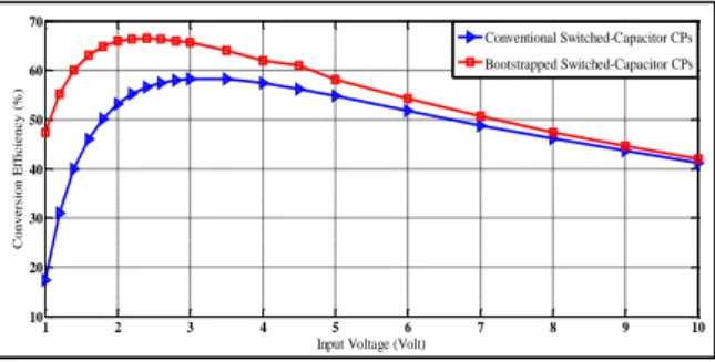
C onv e rs ion E ff ic ie nc y (% ) Conventional Switched-Capacitor CPs Bootstrapped Switched-Capacitor CPs
Figure 14. Variation of the power efficiency versus the input voltage of both the switched–capacitor CPs circuits when C = 10 pF, Io = 500 µA, and f = 50 MHz.
2 3 4 5 6 7 8 9 10 x 108 10 20 30 40 50 60 70 80 Frequencies (Hz) C onv e rs ion E ff ic ie nc y (% ) Conventional Switched-Capacitor CPs Bootstrapped Switched-Capacitor CPs
Figure 15. Simulated efficiency variation versus input frequency for conventional and bootstrapped CPs circuits with C = 10 pF, Io = 500 µA, and VDD = 2 V.
0 0.1 0.2 0.3 0.4 0.5 0.6 0.7 0.8 0.9 1 x 10⁻³ 0 10 20 30 40 50 60 70 80 90
Output Current (Io)
C onv e rs ion E ff ic ie nc y (% ) Conventional Switched-Capacitor CPs Bootstrapped Switched-Capacitor CPs
Figure 13. Simulated between conversion efficiency and variation of the load current of conventional and bootstrapped switched–capacitor CP with C = 10 pF, f=50 MHz, and VDD = 2 V.
VI.
C
ONCLUSIONA high efficiency charge pump circuit is realized in this work. The bootstrapped capacitors and charge transfer switches (transistors) are used to dynamically bias so that they eliminate the drop in the threshold voltage of each transfer switch transistor and improve the pumping efficiency for these proposed circuits. 0.5-μm CMOS process is used to design and simulate the conventional and bootstrapped switched-capacitor CPs circuits. The realization and implementation of all these CPs circuits was computed using OrCad Cadence PSPICE simulation. The simulated results show that the voltage at the output terminal of the five-stage switched-capacitor circuits was 8 V. In this paper, the pumping capacitors of the proposed CPs circuits are 10 pF, the input power supply
voltage is 2 V, the output current is 1 mA, and the clock input frequency is 50 MHz. The bootstrapped technique which implemented for the all CPs circuits has good efficiency about (68.5 %) compared with (53 %) for conventional CPs circuit at pump capacitance of 10 pF, loading current of 500 µA, clock frequency of 50 MHz and supply voltage 2 V.
R
EFERENCES[1] STARZYK, J.A., JAN, Y.-W., and QIU,
F. (2001) A DC-DC Charge Pump
Design Based On Voltage Doublers.
IEEE Transactions on Circuits and
Systems—I: Fundamental Theory and
Applications, 48(3), pp. 350-359.
[2] GREGOIRE, B.R. (2006) A Compact
Switched Capacitor Regulated Charge
Pump Power Supply. IEEE Journal of
Solid-State Circuits, 41(8), pp.
1944-1953.
[3] CABRINI, A., GOBBI, L., and TORELLI,
G.
(2007)
Design
of
Maximum-Efficiency Integrated Voltage Doubler.
Proceedings of the IEEE International
Symposium on Circuits and Systems. pp:
317-320.
[4] MODI, P. (2012) A Charge Pump
Architecture with High Power-Efficiency
and Low Output Ripple Noise in 0.5 µm
CMOS Process Technology. Master
Thesis. Department of Electrical and
Microelectronics Engineering, Rochester
Institute of Technology. pp: 1-83.
[5] HSU, C.-P. and LIN, H. (2010) Analytical
Models of Output Voltages and Power
Efficiencies
for
Multistage
Charge
Pumps. IEEE Transactions on Power
Electronics, 25(6), pp. 1375-1385.
[6] SALMAN, A.D., KHALAF, O.I., and
ABDULSAHIB,
G.M.
(2019)
An
adaptive intelligent alarm system for
wireless sensor network. Indonesian
Journal of Electrical Engineering and
Computer Science, 15(1), pp. 142-147.
[7] PALUMBO, G., PAPPALARDO, D., and
GAIBOTTI, M. (2002) Charge Pump
Circuits:
Power
Consumption
Optimization. IEEE Transactions on
9