Digitally-Assisted Compensation for Timing Skew in ATE Systems
K. Asami T. Tateiwa T. Kurosawa H. Miyajima H. Kobayashi
Advantest Corporation
Gunma University
Contents
• Research Goal
• Conventional Linear Phase Digital Filter Condition
• New Linear Phase Digital Filter Condition
– Time-Shift, Impulse Response of Ideal Filter – New Linear Phase Digital Filter
• MATLAB Simulation
• Design Considerations – Window
– Gain Adjustment
• Application
• Conclusion
Timing skew is a major problem in ATE systems
Digital compensation for timing skew
⇒ Linear phase is important
Conventional linear-phase digital filter ⇒ coarse timing adjustment Proposed linear-phase digital filter ⇒ fine timing adjustment
Research Goal
Fine time resolution
Linear phase (to preserve waveform in time domain)
Applicable to bandpass signal (as well as lowpass signal)
Features of Proposed Digital Filter
τ Fine time shift
F(t)
F(t-τ)
Contents
• Research Purpose
• Conventional Linear Phase Digital Filter Condition
• New Linear Phase Digital Filter Condition
– Time-Shift, Impulse Response of Ideal Filter – New Linear Phase Digital Filter
• MATLAB Simulation
• Design Consideration – Window
– Gain Adjustment
• Application
• Conclusion
Linear Phase FIR Filter Impulse Response
0 3 6
0 3
6
0 3 7
0 3
7 (1)Case 1
odd # of taps ・even symmetry
(2) Case 2
even # of taps ・ even symmetry
(3) Case 3
odd # of taps ・ odd symmetry
(4) Case 4
even # of taps・odd symmetry 4
4
Frequency Characteristics
Case 1
Case 2
Case 3
Case 4
Phase : proportional to ω (linear phase)
Time resolution of group delay T s/2
Contents
• Research Purpose
• Conventional Linear Phase Digital Filter Condition
• New Linear Phase Digital Filter Condition
– Time-Shift, Impulse Response of Ideal Filter – New Linear Phase Digital Filter
• MATLAB Simulation
• Design Consideration – Window
– Gain Adjustment
• Application
• Conclusion
Ideal LPF
: Sampling Frequency Frequency Characteristics
1.0
Impulse Response
Fourier Transform
1 2 3 4 5
-5 -4 -3 -2 -1
Discrete-Time Representation of Ideal LPF
1 2 3 4 5 -5 -4 -3 -2 -1
Fourier Transform
FIR (Finite Impulse Response)
zero
Impulse Response Time-Shift
1 2 3 4 5 -5 -4 -3 -2 -1
No change of Gain
Δt time-shift of impulse response
Time-Shift and Filter Coefficients
FIR filter
1 2 3 4 5 -5 -4 -3 -2 -1
IIR Filter
1 2 3 4 5 -5 -4 -3 -2 -1
Time Shift
Ideal Delay-Filter
zero
Contents
• Research Purpose
• Conventional Linear Phase Digital Filter Condition
• New Linear Phase Digital Filter Condition
– Time-Shift, Impulse Response of Ideal Filter – New Linear Phase Digital Filter
• MATLAB Simulation
• Design Consideration – Window
– Gain Adjustment
• Application
• Conclusion
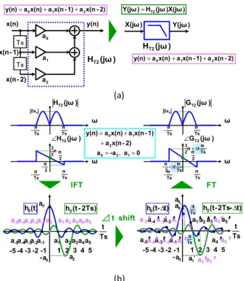
2-Tap Filter: Model
1 0
1 2 3 4 5
-5 -4 -3 -2 -1
2-Tap Filter: Delay Model
0 1
1 2 3 4 5 -5 -4 -3 -2 -1
FIR
IIR
2-Tap Filter: Delay Model
0 1
1 2 3 4 5 -5 -4 -3 -2 -1
IIR
FIR
Proposed Delay Digital Filter
(a) FIR Filter (b) Ideal Delay Filter
(c) Delay Digital Filter
Window
Frequency Characteristics of Proposed Delay Digital Filter
Case 1
Case 2
Case 3
Case 4
Phase : proportional to ω ( linear phase )
Group delay time resolution τ : Arbitrary small
Contents
• Research Purpose
• Conventional Linear Phase Digital Filter Condition
• New Linear Phase Digital Filter Condition
– Time-Shift, Impulse Response of Ideal Filter – New Linear Phase Digital Filter
• MATLAB Simulation
• Design Consideration – Window
– Gain Adjustment
• Application
• Conclusion
Comparison of 2-Tap Filter Impulse Responses
5 10 15 20 25 30
-0.2 0 0.2 0.4 0.6
2 taps FIR Filter
5 10 15 20 25 30
-0.2 0 0.2 0.4 0.6
Delayed Filter (0.3 samples delay)
2-tap FIR coefficients
Impulse response changes.
Proposed Delay Filter ( 0.3 samples delay )
2-Tap FIR Filter
zero
Non-zero
Comparison of
2-Tap Filter Frequency Characteristics
-0.5 0 0.5
-20 -15 -10 -5 0
G a in [ d B ]
-0.5 0 0.5
-2 0 2
Normalized Frequency (Fs=1.0)
P h a se [ ra d ia n ]
No change of gain
Phase slope changes
Proposed delay filter
Original filter
Original filter and
proposed delay filter
Hann window
Finite Tap Truncation of Proposed Delay Filter
10 20 30 40 50 60
-0.2 0 0.2 0.4 0.6
61 taps Cosine Roll-off Filter
10 20 30 40 50 60
-0.2 0 0.2 0.4 0.6
Delayed Filter with Hann window (0.3 samples delay)
61 タップ コサインロールオフフィルタ
10 20 30 40 50 60
-0.2 0 0.2 0.4 0.6
61 taps Cosine Roll-off Filter
10 20 30 40 50 60
-0.2 0 0.2 0.4 0.6
Delayed Filter (0.3 samples delay)
Delay Filter ( 0.3 samples delay ) 61-Tap Cosine Roll-off Filter
Delay Filter ( 0.3 samples delay )
Rectangular
window
Effects of Window
0 0.05 0.1 0.15 0.2 0.25
-10 -5 0
G a in [ d B ]
0 0.05 0.1 0.15 0.2 0.25
30.299 30.2995 30.3 30.3005 30.301
Normalized Frequency (Fs=1.0)
G ro u p D e la y [ sa m p le s]
Hann window
Rectangular window
Frequency characteristics of delay filter with 61-tap truncation
Gibbs oscillation
of group delay
Contents
• Research Purpose
• Conventional Linear Phase Digital Filter Condition
• New Linear Phase Digital Filter Condition
– Time-Shift, Impulse Response of Ideal Filter – New Linear Phase Digital Filter
• MATLAB Simulation
• Design Consideration – Window
– Gain Adjustment
• Application
• Conclusion
How to Apply Window
1 2 3 4 5 -5 -4 -3 -2 -1
Δt T s
1 2 3 4 5 -5 -4 -3 -2 -1
Δt T s
t T s
t T s
Window
Centered at origin
Centered at
impulse response center
Window center shifted by Δt
0 0.1 0.2 0.3 0.4 0.5 -100
-50 0
P o w e r [d B ]
マルチレート・フィルタの周波数特性(非対称)
0 0.1 0.2 0.3 0.4 0.5
-100 -50 0
Normalized frequency
P h a s e [ ra d ]
0 0.1 0.2 0.3 0.4 0.5
-100 -50 0
P o w e r [d B ]
マルチレート・フィルタの周波数特性(対称)
0 0.1 0.2 0.3 0.4 0.5
-100 -50 0
Normalized frequency
P h a s e [ ra d ]
Frequency Characteristics of Delay Filter after Applying Window
Delay 0.3 samples Filter Tap 100 taps
Window Han
Pass band (0.1~0.4)・Fs FFT points 1024 points
Window centered at origin Window centered at impulse response
Ga in[dB ] P has e[d eg ree ]
0.1 0.15 0.2 0.25 0.3 0.35 0.4 49.79
49.795 49.8 49.805
Normalized frequency
G ro u p d e la y
群遅延特性(非対称)
0.1 0.15 0.2 0.25 0.3 0.35 0.4 49.79
49.795 49.8 49.805
Normalized frequency
G ro u p d e la y
群遅延特性(対称)
Group Delay Characteristics of Delay Filter after Applying Window
Window centered at origin Window centered at impulse response
Delay 0.3 samples Filter Tap 100 taps
Window Han
Pass band (0.1~0.4)・Fs
FFT points 1024 points
0 0.1 0.2 0.3 0.4 0.5 -100
-50 0
P o w e r [d B ]
マルチレート・フィルタの周波数特性(非対称)
0 0.1 0.2 0.3 0.4 0.5
-100 -50 0
Normalized frequency
P h a s e [ ra d ]
0 0.1 0.2 0.3 0.4 0.5
-100 -50 0
P o w e r [d B ]
マルチレート・フィルタの周波数特性(対称)
0 0.1 0.2 0.3 0.4 0.5
-100 -50 0
Normalized frequency
P h a s e [ ra d ]
Frequency Characteristics of Delay Filter after Applying Window
gain [d B] Ph ase [d e gr e e ]
Delay 0.3 samples Filter Tap 100 taps
Window Han
Pass band (0.05~0.3)・Fs FFT points 1024 points
Window centered at origin Window centered at impulse response
0.05 0.1 0.15 0.2 0.25 0.3 49.79
49.795 49.8 49.805
Normalized frequency
G ro u p d e la y
群遅延特性(非対称)
0.05 0.1 0.15 0.2 0.25 0.3
49.79 49.795 49.8 49.805
Normalized frequency
G ro u p d e la y
群遅延特性(対称)
Group Delay Characteristics of Delay Filter after Applying Window
Delay 0.3 samples Filter Tap 100 taps
Window Han
Pass band (0.05~0.3)・Fs FFT points 1024 points
Window centered at impulse response
Window centered at origin
0.05 0.1 0.15 0.2 0.25 0.3 49.79
49.795 49.8 49.805
Normalized frequency
G ro u p d e la y
群遅延特性(非対称)
0.05 0.1 0.15 0.2 0.25 0.3
49.79 49.795 49.8 49.805
Normalized frequency
G ro u p d e la y
群遅延特性(対称)
Group Delay Characteristics of Delay Filter after Applying Window
Delay 0.3 samples Filter Tap 100 taps
Window Han
Pass band (0.05~0.3)・Fs FFT points 1024 points
Window centered at impulse response Window centered at origin
Applying window centered at impulse response
Constant group delay over entire passband
Contents
• Research Purpose
• Conventional Linear Phase Digital Filter Condition
• New Linear Phase Digital Filter Condition
– Time-Shift, Impulse Response of Ideal Filter – New Linear Phase Digital Filter
• MATLAB Simulation
• Design Consideration – Window
– Gain Adjustment
• Application
• Conclusion
Proposed Filter DC Gain Adjustment
Digital filter DC gain :
1 2 3 4 5 -5 -4 -3 -2 -1
t T s
Δt T s
a n
a 0 a 1
a 2 a 3
a 4 a 5
a 6
a 7 a 8
a 9
a 10
DC gain adjustment due to finite tap truncation is required
● Original filter
● Delay filter
a ' n
n=0 N
= DC gain of original FIR filter
0 0.1 0.2 0.3 0.4 0.5 -100
-50 0
Normalized Frequency
P o w e r [d B ]
ゲイン未調整
0 0.1 0.2 0.3 0.4 0.5
-150 -100 -50 0
Frequency
P h a s e [ d e g re e ]
0 0.1 0.2 0.3 0.4 0.5
-100 -50 0
Normalized Frequency
P o w e r [d B ]
ゲイン未調整
0 0.1 0.2 0.3 0.4 0.5
-150 -100 -50 0
Frequency
P h a s e [ d e g re e ]
Frequency Characteristics of Proposed Delay Filter
With DC gain adjustment Without DC gain adjustment
Delay 0.3 samples
Filter Tap 101 taps
Window Han
Cut-off Freq. 0.4・Fs
FFTpoints 1024 points
0 0.1 0.2 0.3 0.4 0
0.005 0.01 0.015 0.02 0.025 0.03 0.035 0.04
Normalized Frequency
g a in [ d B ]
マルチレート・フィルタの周波数特性
0 0.1 0.2 0.3 0.4
0 0.005 0.01 0.015 0.02 0.025 0.03 0.035 0.04
Normalized Frequency
g a in [ d B ]
マルチレート・フィルタの周波数特性
Gain Characteristics of Proposed Delay Filter
Delay 0.1samples
Filter Tap 101 taps
Window Han
Cutoff Freq. 0.4・Fs FFTpoints 1024 points
Delay 0.3 samples Filter Tap 101 taps
Window Han
Cutoff Freq. 0.4・Fs FFT points 1024 points
0.005dB 0.0006dB
With DC gain adjustment Without DC gain adjustment
gai n [d B]
0 0.1 0.2 0.3 0.4 0
0.005 0.01 0.015 0.02 0.025 0.03 0.035 0.04
Normalized Frequency
g a in [ d B ]
マルチレート・フィルタの周波数特性
Original FIR filter
With DC gain adjustment Without DC gain adjustment
Gain Characteristics of Proposed Delay Filter
0 0.1 0.2 0.3 0.4
0 0.005 0.01 0.015 0.02 0.025 0.03 0.035 0.04
Normalized Frequency
g a in [ d B ]
マルチレート・フィルタの周波数特性
Delay 0.1samples
Filter Tap 101 taps
Window Han
Cutoff Freq. 0.4・Fs FFTpoints 1024 points
Delay 0.3 samples Filter Tap 101 taps
Window Han
Cutoff Freq. 0.4・Fs
FFT points 1024 points
0 0.1 0.2 0.3 0.4 0
0.005 0.01 0.015 0.02 0.025 0.03 0.035 0.04
Normalized Frequency
g a in [ d B ]
マルチレート・フィルタの周波数特性
Original FIR filter
With DC gain adjustment Without DC gain adjustment
Gain Characteristics of Proposed Delay Filter
0 0.1 0.2 0.3 0.4
0 0.005 0.01 0.015 0.02 0.025 0.03 0.035 0.04
Normalized Frequency
g a in [ d B ]
マルチレート・フィルタの周波数特性
Delay 0.1samples
Filter Tap 101 taps
Window Han
Cutoff Freq. 0.4・Fs FFTpoints 1024 points
Delay 0.3 samples Filter Tap 101 taps
Window Han
Cutoff Freq. 0.4・Fs FFT points 1024 points
DC gain adjustment
Delay filter gain
Original FIR filter gain
Contents
• Research Purpose
• Conventional Linear Phase Digital Filter Condition
• New Linear Phase Digital Filter Condition
– Time-Shift, Impulse Response of Ideal Filter – New Linear Phase Digital Filter
• MATLAB Simulation
• Design Consideration – Window
– Gain Adjustment
• Application
• Conclusion
I/Q Delay Mismatch in Quadrature Modulator
s(t) t
p/2 fc
DAC
DAC I(t) = cos (2pf 0 t)
Q(t) = sin(2pf 0 t) SSB signal input
DAC : digital-to-analog converter SSB : single side band
f c I(t)+jQ(t)
0 f c - f 0 f c +f 0
f f
delay
in analog domain
Image
rejection
ratio
I/Q Delay Mismatch Compensation in Quadrature Modulator
s(t) t
p/2 fc
DAC
DAC I(t) = cos (2pf 0 t)
Q(t) = sin(2pf 0 t) SSB signal
DAC : digital-to-analog converter SSB : single side band
f c I(t)+jQ(t)
0 f c - f 0 f c +f 0
f f
Delay
in analog domain
digital timing
compensation τ
Matlab Simulation Results
(b) Timing skew case
Delay 0.3 samples Filter tap # 61 taps
Window Han
FFT points 1024 points
-0.5 0 0.5
-140 -120 -100 -80 -60 -40 -20 0
Normalized frequency
M a g n it u d e [ d B ]
タイミング・スキューのある信号 image signal
-0.5 0 0.5
-140 -120 -100 -80 -60 -40 -20 0
Normalized frequency
M a g n it u d e [ d B ]
理想信号
(a) Ideal case
signal
Matlab Simulation Results
-0.5 0 0.5
-140 -120 -100 -80 -60 -40 -20 0
Normalized frequency
M a g n it u d e [ d B ]
ゲイン無調整
(c) Compensation using delay filter
Without adjustment of window, gain
signal image
-0.5 0 0.5
-140 -120 -100 -80 -60 -40 -20 0
Normalized frequency
M a g n it u d e [ d B ]
ゲイン改善 signal image
Delay 0.3 samples Filter tap 61 taps
Window Han
FFT points 1024 points
(d) Compensation using delay filter
With adjustment of window, gain
M channel ADCs M-times sampling rate
Interleaved ADC System
ADC : analog-to-digital converter
ADC1 M
U X
CLK1
CLK2
ADC2
T s
t CLK 1
CLK 2
Timing Skew in Interleaved ADC System
f in F s - f in F s f
f in f 0
0
Analog Input
F s =1/T s F s
f in
Digital output
D out
ADC : analog-to-digital converter
ADC1 M
U X
CLK1
CLK2
ADC2
T s
t CLK 1
CLK 2
Timing Skew Compensation in Interleaved ADC System
f in f
f in f 0
0
F s =1/T s F s
F s - f in F s
Analog input
f in Clock skew effect
compensation
Digital output
D out
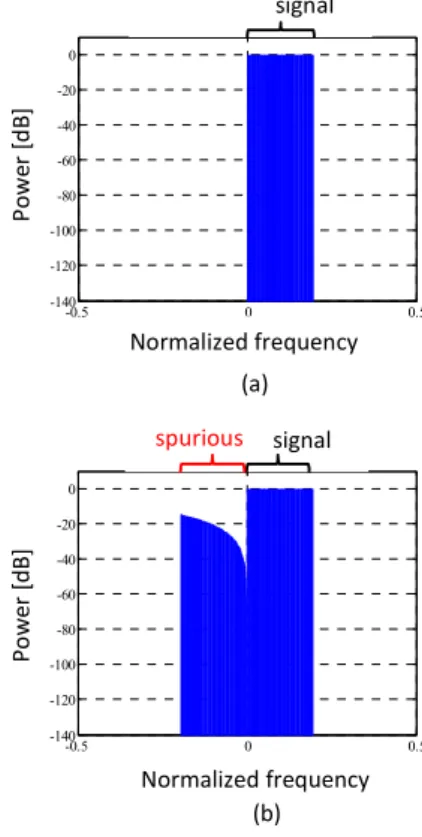
Matlab Simulation Results
0 0.1 0.2 0.3 0.4 0.5
-120 -100 -80 -60 -40 -20 0
Normalized frequency
M a g n it u d e [ d B ]
スキューのある信号
0 0.1 0.2 0.3 0.4 0.5
-120 -100 -80 -60 -40 -20 0
Normalized frequency
M a g n it u d e [ d B ]
スキューのある信号
Signal Signal Spurious
Delay 0.3 samples Filter tap 61 taps
Window Han
FFTpoints 1024 points
(a) Ideal case (b) Timing skew case
0 0.1 0.2 0.3 0.4 0.5 -120
-100 -80 -60 -40 -20 0
Normalized frequency
M a g n it u d e [ d B ]
補正後のスペクトラム
0 0.1 0.2 0.3 0.4 0.5
-120 -100 -80 -60 -40 -20 0
Normalized frequency
M a g n it u d e [ d B ]
補正後のスペクトラム
Matlab Simulation Results
Delay 0.3 samples Filter tap 61 taps
Window Han
FFTpoints 1024 points
Signal Spurious Signal Spurious
(c) Compensation using delay filter
Without adjustment of window, gain
(d) Compensation using delay filter
With adjustment of window, gain
Conclusion
● Linear phase digital filter
with fine time resolution of group delay
● Design consideration - How to apply window - DC gain adjustment
● Application Examples
- I/Q delay mismatch compensation in quadrature modulator
- Timing skew compensation in interleaved ADC system On-going work
● Implementation issues
– Finite word length, finite tap effects
– LSI implementation
Digitally-Assisted Compensation Technique for Timing Skew in ATE Systems
Koji Asami ∗, Takenori Tateiwa, Tsuyoshi Kurosawa Hiroyuki Miyajima, Haruo Kobayashi
∗ Advantest Corporation, Meiwa-machi, Ora-gun, Gunma 370-0718 Japan
Dept. of Electronic Engineering, Gunma University, Kiryu, Gunma 376-8515 Japan
Email: [email protected], [email protected]
Abstract
This paper describes timing skew adjustment techniques in ATE systems (such as for timing skew compensation in an interleaved ADC system and an SSB signal generation system) using a digital filter with novel linear phase condition proposed in our ITC2010 paper. A conventional linear phase digital filter is an FIR filter with coefficients of odd- or even –symmetry and whose group delay NTs/2 where N is the number of the FIR filter taps and Ts is the sampling period; its group delay time resolution is Ts/2. We have generalized the linear phase condition, and with our novel linear phase condition, the group delay time resolution can be arbitrary small, and the coefficients are not necessarily odd- or even-symmetric. In this paper we discuss several practical issues for applying our digital filter to timing skew compensation in ATE systems, such as truncation of the infinite number of taps, techniques of using window and DC gain adjustment. We also compare our digital filter with the fractional delay digital filter.
Keywords: Digital Filter, Linear Phase, Digitally- Assisted Analog Technology, Timing Skew, ATE, Fractional Delay Digital Filter
1. Introduction
In this paper we describe a digital filter with novel linear phase condition and show that its delay time resolution is arbitrary fine (i.e., its group delay can be set with arbitrary small time resolution), and its practical issues for timing skew adjustment applications in ATE systems.
In section 2, conventional linear phase condition for digital filter is explained, and in section 3, our novel linear phase condition is explained based on our ITC2010 paper [1]. In section 4, we investigate realization consideration for our digital filter, and in section 5, comparison with fractional delay filter is shown. Section 6 concludes the paper.
2. Conventional Linear Phase Condition
Linear phase characteristics are important for the digital filter to preserve the signal waveform in time domain. It is well-known in [2-4] that the FIR digital filter with odd or even symmetry coefficients has linear phase characteristics and it is unconditionally stable. The IIR digital filter with odd or even symmetry of both its denominator and numerator has also linear characteristics but it is unstable. Hence in almost all
cases, the FIR digital filter with odd or even symmetry coefficients is used where the linear phase is required, and in such cases its group delay is (N/2)Ts where N is the number of the FIR filter taps and Ts is the sampling period; in other words the time resolution of the group delay is Ts 2, and this cannot be used for fine timing skew adjustment in ATE systems.
3. Novel Linear Phase Condition
In this section, we describe - based on our ITC2010 paper [1] - the extended linear phase characteristics conditions for the digital filter which has not necessarily odd or even symmetry coefficients, and its time resolution of the group delay is arbitrary small.
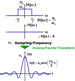
First we discuss without consideration of causality, for simplicity. Let us consider the following analog filter (Fig.1):
( )
⎩⎨
⎧ − < <
= 0 otherwise.
T case
in s
0 in
π
sω π
out
T t
v
v a (1)
Then its impulse response h(t) is given as follows:
( )
t a0Tssinc(
t Ts)
.h =
π
(2) We consider the case that the input vin( )
t is band-limited to −π Ts<ω<π Ts . We sample the above impulse response with a period Ts, and use the following transformation to obtain the digital filter which corresponds to the analog filter in (1):( ) ( )
( ) ( )
.1 n x nT v
n y nT v
T
s in
s out
s
→
→
→
(3)
Then we have the following digital filter:
( )
n ax( )
ny = 0 (4) This is because
( )
⎩⎨⎧ == 0 otherwise 0 case in
sinc 1 n
πn (5)
This digital filter has obviously linear phase characteristics (or rigorously speaking zero phase characteristics).
IEEE International Mixed-Signals, Sensors, and Systems Test Workshop 16 - 18 May 2011, Santa Barbara, CA
⎟⎠
⎜ ⎞
⎝
= ⎛ t
2 sinc ω a
h(t) 0 S
Inverse Fourier Transform h(t)
t a0
2 ωS s 0
ω a
ω ) H(jω
2 -ωS
ω )
∠H(jω
0 ) Hjω =
∠
s 0
ω ) a H(jω =
ωs:Sampling Frequency
Fig. 1. An ideal analog low pass filter. Gain, phase characteristics, and impulse response.
⎟⎠
⎜ ⎞
⎝
⎛ Δ
= Δ
=
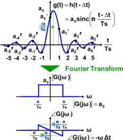
Ts t - sinc t a
t) - h(t g(t)
0 π
Ts t a0
1 2 3 4 5 -5 -4 -3 -2 -1
a-5’a-3’ a-2’ a-1’
a1’ a2’
a3’ a4’
a5’ a-4’
0' a
Ts Δt
Ts π
a0
ω ) G(jω
-Tsπ
Fourier Transform
Δt -ω ) G(jω =
∠
a0
) G(jω =
Ts π
ω )
∠G(jω
-Tsπ tTs - π Δ
tTsπ Δ
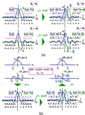
Fig. 2. Sampling timing shift can maintain the linear phase characteristics. Impulse response, and gain, phase characteristics.
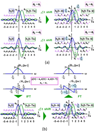
Now let us consider to sample h
( )
t at t=nTs+τ (Fig.2), where 0<τ<Ts, and use (3). characteristics). Then we have the following digital filter which corresponds to the analog filter in (1):( )
n a x(
n k)
.y
k
k −
=
∑
∞ ′−∞
=
(6) Here
( )
( )
.sinc s
k k T
a′ =
π
+τ
(7) In general ak′ is not necessarily zero and ak′ is not necessarily equal to a−′k or −a−′k.Proposition 1 : The digital filter given by (6), (7) has the linear filter characteristics, and its group delay is τ.
Next we discuss in case of Fig.3, and consider the following analog filter:
( ) ( )
⎪⎩
⎪⎨
⎧
<
<
−
− +
=
otherwise.
0
case in
1 0
T T
T t v a t v a
v s
s in in
out
π ω π
(8)Note that its impulse response is given as follows:
( )
t =a0Tssinc(
t Ts)
+a1Tssinc( (
t Ts−1) )
.h
π π
(9)We assume that the input vin
( )
t is band-limited tos
s T
T ω π
π < <
− . Similarly we sample this filter with nTs
t= , and we have the following digital filter using (3):
( )
n =a0x( )
n +a1x(
n−1)
.y (10)
Next we sample (9) with t=nTs+τ, and we have the following digital filter:
( ) ∑
∞( )
.−∞
=
′ −
=
k
kxn k
a n
y (11) Here
( )
( )
sinc( ( (
1) ) )
.sinc 1
0 s s
k a k T a k T
a′ = π +τ + π − +τ (12)
Proposition 2 : The digital filter given by (11), (12) with a0=a1 or a0=−a1 has the linear phase characteristics and its group delay is Ts 2+τ. Also the digital filter of (11) has the same gain characteristics as (10). The same argument holds for an N-tap FIR filter.
Proposition 3 : Let us consider an N-tap FIR digital filter with coefficients ak of odd or even symmetry.
( ) ∑
−( )
=
−
= 1
0 N
k
kx n k
a n
y (13) Then the following digital filter has the linear characteristics with group delay
(
N 2)
Ts+τ.( ) ∑
∞( )
−∞
= ′ −
=
k
kx n k
a n
y (14) Here
( )
( )
( )
.sinc
1
∑
−0=
+
−
′ =N
l
s l
k a k l T
a
π τ
(15)Table 1 shows the frequency characteristics of digital filters with our proposed linear phase condition.
TABLE I Frequency characteristics of the proposed linear phase digital filter
IEEE International Mixed-Signals, Sensors, and Systems Test Workshop 16 - 18 May 2011, Santa Barbara, CA
(a)
(b)
Ts t 1 2 3 4 5 -5 -4 -3 -2 -1
a-5a-4a-3a-2a-1 a1a2a3a4a5
a1
a-5a-4a-3a-2a-1a0 a2a3a4a5 (t)
h0 h1(t-Ts)
FT IFT
⊿t shift
1 0
1 0
a a
1) - x(n a x(n) a y(n)
= +
=
Ts t 1 2 3 4 5 -5 -4 -3 -2 -1
a-5’ a-3’ a-2 ’
a-1 ’ a1’a2 a’3 ’a4 ’a5 ’ a-4 ’
a-5’ a-3’ a-2’
a-1 ’ a0’
a2’ a3’a4’a5’ a-4’
t) - (t
h0 Δ TsΔt a1' h1(t-Ts-Δt)
Ts Δt
a0 Ts
π 2a0
ω ) (jω HT1
-Tsπ
Ts π
ω ) (jω HT1
∠
-Tsπ -π2 2
π
Ts
π ω
) (jω GT1
-Tsπ
Ts
π ω
) (jω GT1
∠
-Tsπ tTs 2-
-π π
Δ tTs 2
π π+Δ 2a0
a0 a0’
Ts t 1 2 3 4 5 -5 -4 -3 -2 -1
a-5a-4a-3a-2a-1 a1a2a3a4a5
a1
a-5a-4a-3a-2a-1a0 a2a3a4a5
(t)
h0 h1(t-Ts)
Ts t 1 2 3 4 5 -5 -4 -3 -2 -1
a-5a-4a-3a-2a-1 a1a2a3a4a5
a1
a-5a-4a-3a-2a-1a0 a2a3a4a5
(t)
h0 h1(t-Ts)
1 0 a a=
1 0 -a a=
1 0 a a=
Ts t 1 2 3 4 5 -5 -4 -3 -2 -1
a-5’ a-3’ a-2 ’
a-1 ’ a1’a2 ’a3 ’a4 ’a5 ’ a-4 ’
a-5’ a-3’ a-2’
a-1 ’ a0’
a2’ a3’a4’a5’ a-4’
t) - (t
h0 Δ Ts h1(t-Ts-Δt)
Δt a1'Ts
Δt
a0
1 0 -a a=
Ts t 1 2 3 4 5 -5 -4 -3 -2 -1
a-5’ a-3’ a-2 ’
a-1 ’ a1’a2 ’
a3 ’a4 ’a5 ’ a-4 ’
a-5’ a-3’ a-2’
a-1 ’ a0’
a2’ a3’a4’a5’ a-4’
t) - (t
h0 Δ Ts h1(t-Ts-Δt)
Δt
1' a TsΔt a0
⊿t shift
⊿t shift a0
a0’ a1’
Fig. 3. 2-tap FIR filter without and with sampling timing shift. (a) Impulse response. (b) Gain and phase responses.
Now we will provide the proof for our proposed linear phase digital filter in general case: let us consider an N- tap FIR filter with conventional linear phase condition, and we have the impulse response h~
( )
t with continuous time and its Fourier transform H~( )
f :( ) ( ) ( )
.~ 1
∑
−0=
−
=N
n
s
s t nT
nT h t
h
δ
(16)( ) ( )
1 ( .)~
∑
∞−∞
= −
=
k Ts
f k f T
H f
H ★
δ
(17)Here ⋆ indicates convolution, δ
( )
⋅ denotes a delta function, and( ) ( )
2 21 ( 21 21 ).s s
N T f j
f T e T
f H f
H = − π − s − ≤ ≤ (18)
When we add a delay τ to the impulse response h
( )
tand we have its frequency characteristics as follows:
( )
f H( )
f e j2πfN21T e j2πfτ.H s −
− −
⋅
′ = (19)
We see that the phase characteristics of H′
( )
f is linear with respect to f . H′( )
f can be interpreted as the convolution between H( )
f and S( )
f , where S( )
f is theideal filter with a delay τ:
( )
2 21 ( 21 21 ).s s
fN j
f T e T
f
S = − ≤ ≤
− π −τ
(20)
Thus after the sampling operation in time domain, the ideal filter S
( )
f in Eq.(20) leads to the following S~( )
f :( ) ( )
( ) ( .)~
∑ ∑
∞−∞
=
∞
−∞
=
−
=
−
=
k s
k s T
f k T S
f k f
S f
S ★
δ
(21)Next we will consider the effect of the delay τ to the impulse response. The inverse Fourier transform of
( )
fS~ is given as follows:
( ) ( )
( )
.)) ( (
sinc )) ( (
~ sinc
∑
∑
∞
−∞
=
∞
−∞
=
− −
=
−
− ⋅
=
n
s s
n
s s
nT T t
t
nT T t
t t s
τ δ π
τ δ π
(22)
We see from (22) that ~s
( )
t is asymmetric with respect to=0
t , and we have the following impulse response:
Thus the impulse response of time delay τ with continuous time has finite values for t→±∞ due to the sinc function effects.
4. Realization Consideration
We sample the input signal with the sampling period Ts and then we consider the band-limited case to
s
s T
T ω π
π < <
− , in order to avoid the aliasing effects.
In such case h
( )
t does not converge to zero as t becomes plus/minus infinity. So the digital filter with our novel linear phase condition has to have the infinite number of taps and this cannot be realized. (Note that in case ofτ=0, h( )
nTs can be zero as n becomes large which corresponds to the conventional linear phase FIR digital filter case.) So we consider to truncate the terms for large number of k in (15) applying a window function and we approximate the digital filter of (14), (15) with the finite number of taps. We also consider here the DC gain adjustment.4.1 Approximation with Finite Number of Taps The ideal digital filter with our proposed linear phase condition needs infinite number of taps. However it is cannot be realized, and hence we have to approximate it as the filter with finite number of taps. We consider here the effects of the truncation to the finite number of taps.
We observe from our simulation results so-called Gibbs oscillation at the edges of pass-band of the gain characteristics and also phase characteristics (Fig.4) [2], [3]; Gibbs oscillation for phase characteristics is not observed in many cases, and we have found that this Gibbs oscillation for phase characteristics is due to the asymmetry of the impulse response h
( )
n with respect to=0 n .
h t
( )
C s t( )
= h nT
( )
s δ(
t−nTs)
Cn=0 N−1
∑
sinc(π(kTTs−τ)s
)⋅δ
(
t−nTs)
n=−∞
∑
∞= h nT
( )
sn=0
∑
N−1 sinc(π(kTTs−τ) s)⋅δ
(
t−(
n−k)
Ts)
n=−∞
∑
∞ . (23)IEEE International Mixed-Signals, Sensors, and Systems Test Workshop 16 - 18 May 2011, Santa Barbara, CA
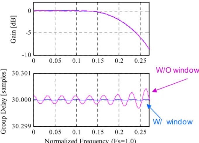
0 0.05 0.1 0.15 0.2 0.25 -10
-5 0
Gain [dB]
0 0.05 0.1 0.15 0.2 0.25 30.299
30.000 30.301
Normalized Frequency (Fs=1.0)
Group Delay [samples] W/O window W/ window
Fig. 4. Gain and phase characteristics of the proposed digital filter (with time shift τ of 0.3Ts) after truncation to finite number (N=61) of filter taps with and without applying Hann window.
4.2 Applying Window Function
Next we investigate to use window functions when we approximate the ideal filter using the one with the finite number of taps. When we use a window function, the Gibbs oscillations for gain and phase are suppressed.
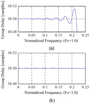
Fig.5 shows our simulation result with time-shift τ of 0.3Ts and applying Hann window. We have also found that this Gibbs oscillation for phase can be further suppressed if we use a window function with the time- shift τ, as shown in Fig.5 where we choose the time shift τ of 0.5Ts (which affects phase characteristics significantly) and we use a Hann window.
There can be two methods for applying a window: one is to use the window with symmetry to the Y-axis (Fig.5 (a)) and the other is to use the window with the symmetry to the center of the impulse response (Fig.5 (b)). We have performed simulation and found that the one in Fig.5 (b) is better. The Gibbs oscillation of the group delay is suppressed when the window of time- shift is used for the LPF (Fig.6).
Our proposed linear phase filter is also applicable to a bandpass filter and Fig.7 shows the group delay of the bandpass filter with the bandwidth of 0.1 fs – 0.4fs. We see that the group delay is almost constant in the wider range when the window of time-shift is used (Fig.7 (b)).
4.3. DC Gain Adjustment
The DC gain of our digital filter can be changed by truncation to the finite number of the taps after windowing, and we have to adjust it for the practical use.
The DC gain adjustment technique can be described as follows:
1 2 3 4 5 -5 -4 -3 -2 -1
1 2 3 4 5 -5 -4 -3 -2 -1
Δt Ts Δt Ts
t Ts
t Ts Window
(a)
(b)
Fig.5. (a) Window with symmetry to the Y-axis (window is not time-shifted). (b) Window with
symmetry to the center of the impulse response (window is time-shifted).
0 0.05 0.1 0.15 0.2 0.25
30.48 30.50 30.52
Normalized Frequency (Fs=1.0)
Group Delay [samples]
0 0.05 0.1 0.15 0.2 0.25
30.48 30.50 30.52
Normalized Frequency (Fs=1.0)
Group Delay [samples] (a)
(b)
Fig.6. Group delay characteristics of the proposed digital filter (with time shift τ of 0.5Ts) after truncation to finite number (N = 61) of filter taps. (a) With applying Hann window of no time-shift. (b) With applying Hann window time-shifted by τ =0.5Ts
Our digital filter without DC gain adjustment g(n) = h(n) where n= 0, ±1, ±2, ±3,…±N Our digital filter with DC gain adjustment
g’(n) = (Gideal / Gfnt ) h(n)
where n= 0, ±1, ±2, ±3,…±N Here DC gain of the ideal filter is given by Gideal =
∑
∞( )
−∞
= n
n h