INVITED PAPER
Special Section on Fundamentals and Applications of Advanced Semiconductor DevicesIntegration of Chemical Sensors with LSI Technology — History and Applications —
Agn`es TIXIER-MITA†∗a), Takuya TAKAHASHI††,Nonmembers,andHiroshi TOSHIYOSHI†∗,Member
SUMMARY Chemical sensors are one of the oldest fields of re- search closely related to the semiconductor technology. From the Ion- Sensitive Field-Effect Transistors (ISFET) in the 70’s, through Micro- Electro-Mechanical-System (MEMS) sensors from the end of the 80’s, chemical sensors are combining in the 90’s MEMS technology with LSI intelligence to devise more selective, sensitive and autonomous devices to analyse complex mixtures. A brief history of chemical sensors from the ISFET to the nowadays LSI integrated sensors is first detailed. Then the states-of-the-art of LSI integrated chemical sensors and their wide range of applications are discussed. Finally the authors propose a brand-new usage of integrated wireless MEMS sensors for remote surveillance of chemi- cal substances, such as food-industry or pharmaceutical products, that are stored in closed environment like a bottle, for a long period. In such en- vironment,in-situanalyse is necessary, and electrical cables, for energy supply or data transfer, cannot be used. Thanks to integrated MEMS, an autonomous long-termin-situquality deterioration tracking system is pos- sible.
key words: chemical sensors, MEMS technology, MEMS LSI integration, monolithic integration, wireless sensors
1. Introduction
Chemical sensors are one of the oldest fields of research closely related to the semiconductor technology. The earli- est types of chemical sensors realized in silicon technology were based on field-effect transistors (FETs), and began to emerge in the 1970’s with Ion-Sensitive Field-Effect Tran- sistors (ISFET), often used for pH sensing. The 1980’s saw the miniaturization of standard chemical analyses systems, like electrochemical sensors. Actually, thanks to the emer- gence of the Micro-Electro-Mechanical-System (MEMS) technology, closely related to the rapid development of the Integrated Circuits fabrication industry, new type of chemi- cal sensors appeared.
However several problems with chemical sensors re- mained unsolved: how to make truly reliable and generic chemical sensors, selective and sensitive enough to analyse complex mixtures or low concentrations?
To try to answer this question, sensor arrays in the 90’s began to emerge: array of functionalized sensors were real- ized to enhance the analyse of more complex mixtures. In
Manuscript received August 25, 2011.
Manuscript revised December 7, 2011.
†The authors are with the Institute of Industrial Sciences, The University of Tokyo, Tokyo, 153-8505 Japan.
††The author is with the Research Center for Advanced Science and Technology, The University of Tokyo, Tokyo, 153-8505 Japan.
∗Presently, with Research Center for Advanced Science and Technology, The University of Tokyo.
a) E-mail: [email protected] DOI: 10.1587/transele.E95.C.777
parallel, data processing with integrated (or not) LSI was in- troduced to manage the huge number of data coming from the array. Such development then opened the door to elec- tronic noses and tongues for food-processing industry and laboratory-on-chip for medical applications.
Three very interesting publications have already re- viewed chemical sensors integrated with LSI devices, from the 90’s to today [1]–[3]. So the purpose of this paper is not to detail the state of the art of this field, already developed so far in these publications. The authors will aim at first to give an overview of the history, the principle, the fields of applications, and then the perspectives in the future of LSI integrated chemical sensors. Finally, to illustrate their point, the authors will propose a wireless chemical sensor to be used in closed containers.
2. Brief History of Chemical Sensors
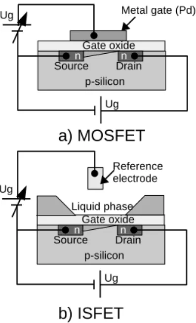
“Chemical sensors” is an old field of research which began at the beginning of the 20th century with pH glass electrodes and ion-exchange theory [4]. Despite this long history, re- search in this field did not at all reached its end, and still remains as a hot topic which has taken the advantages of the revolution brought by the microelectronics technology huge development. Actually, the beginning of the 70’s saw the start of the miniaturization and the introduction of mi- croelectronics in chemical sensors, thanks to the discovery of the ISFET (Ion Sensitive Field Effect Transistor) as a pH sensor by Bergveld [5], [6].
The ISFET is in fact nothing else than a MOSFET (Metal Oxide Semiconductor Field-Effect Transistor), with the gate connection separated from the chip, in the form of a reference electrode inserted in an aqueous solution, which is in contact with the gate oxide (Fig. 1) [7]. From that mo- ment a multitude of derivates form ISFET chemical sensors appeared, which differ one from the other by the sensitive layer on top of the ISFET: CHEMFET, or chemically sensi- tive FET, with an organic-ion selective membrane for ion de- tection (like K+, Na+or Ag+) [8]; immunoFET, with mem- branes with antibodies for immunoreactions detection; EN- FET, with specific enzymes incorporated inside the mem- brane for biochemical compounds analyse (ex: glucose);
etc. In 1983, Kurare Ltd. began the first commercialization of ISFET as pH and CO2 clinical monitors, for catheters applications [9]. It was followed in 1986 by Thorn EMI Mi- crosensor.
To understand better the orientation of the chemical re- Copyright c2012 The Institute of Electronics, Information and Communication Engineers
search field, it is important to point out the desired proper- ties of such systems. The most important parameters to be considered are the high selectivity and sensitivity, and the high reversibility [10]. Until the end of the 70’s the research and development was dedicated mainly to selective sensors that would be able to detect only one single compound in a mixture (ex: pH). Effort has been made to develop sensi- tive layers to be placed on the sensor, which role is, like a filter, to interact selectively with one certain compound (for instance silicon nitride used to detect protons in pH-FET).
A selective layer can, for instance, change its physical char- acteristics (like resistivity, or resonant frequency) due to the absorption of some compounds. This kind of highly specific sensor is referred to as a “zero-order device” [11].
However, ensuring a good selectivity as well as a good reversibility of the sensor is contradictory, because high se- lectivity implies strong interactions of the compounds with the sensitive layer, while reversibility implies weak interac- tions. A compromise has to be found, reducing at the same time the degree of selectivity of the sensor, and increasing the sensitivity to interferents. It means that with such zero- order system reliable analyte quantification cannot be per- formed, as interference with other compounds is unavoid- able.
From the beginning of the 80’s a new concept was pro- posed in order to overcome the problems of selectivity. This is the concept of “sensor arrays”. Instead of having a highly specific sensor, an array of non-specific different sensors is used, which effectively extends the “feature space” (sensor measurement values). The acquired information is then pro- cessed using pattern recognition and multicomponent anal- ysis tools [12]. With sensor arrays substantial improvement
Fig. 1 Scheme of a MOSFET (a) and an ISFET (b) devices. Ug is the gate voltage and Ud the source drain voltage. In the ISFET, the metal gate of the MOSFET is replaced by an ionic solution and a reference electrode placed inside this solution [7].
in analytical capabilities can be realized [13]. A first order sensor array and a second order device can be distinguished according to if the sensors differ in one domain (array of same sensors but differing from the type of sensitive layer) or two domains (array of different types of sensors combined with different types of sensitive layers) [14], [15]. A second order device remains preferable, because with a first order device interferences can be detected but not compensated for.
Based on this new concept of sensor arrays, in 1982 the
“Electronic Nose” and later in 1995 the “Electronic Tongue”
systems began to emerge [16]. From the middle of the 80’s sensor arrays became very popular. The interest for more reliable systems, even if more complex, was also stimu- lated by the increasing need of chemical sensors in variety of industrial and environmental applications: food-industry, biomedical applications, environment and safety.
From the technological point of view, the rapid de- velopment of the CMOS (Complementary-Metal Oxide- Semiconductor) technology as well as the good mechani- cal properties of silicon have lead to two big consequences:
the birth of Micro Electro Mechatronics Systems (MEMS), and the development of intelligent systems through LSI sys- tems. Thanks to MEMS, new types of chemical sensors saw the light (mass, thermal, capacitive sensors and so on).
Thanks to LSI systems development, it became possible to process the complex data coming from sensor arrays, help- ing at the same time to develop more intelligent, compact, autonomous and reliable sensors in a generic approach. LSI can be integrated in an hybrid or a monolithic way.
3. Hybrid Versus Monolithic Integration
When talking about integration of sensors with LSI technol- ogy, it can be either hybrid integration of discrete sensors or monolithic integration (Fig. 2). The choice between them depends on several considerations, as detailed in Table 1 [17].
To summarize the table, the main disadvantage of monolithic integration is the restriction in materials and the limited choice of fabrication processes and steps. On the other hand, regarding all other considerations, it offers unprecedented advantages compared to hybrid integration, especially for signal quality, device performance and in- creased functionality, helping at the same time costs reduc- tions [18].
Fig. 2 (a) Hybrid integration versus (b) monolithic integration.
Table 1 Advantages and disadvantages between hybrid and monolithic integration.
Hybrid Monolithic
(−)Restricted to CMOS Materials (+)No restriction technology compatible
process and materials Performance (−)Many wiring (+)On-chip electronics:
with parasitic effect parasitic effect reduced Auxiliary (−)Additional (+)On-chip calibration, Sensors/ devices, off-chip control, signal Smart Features components required. and processing.
Connectivity (−)Many connections (+)Few connections Sensor Response (−)Chamber volume (+)Smaller size: small Time (dependent dependent on sensor volume of measurement
on measurement geometries. chamber.
chamber volume)
(−)Complex (+)Microelectronics-
Package packages derived packaging
techniques.
4. Principle of LSI Integration
Hybrid integration of chemical sensor with LSI still remains the preferred integration procedure, as it needs simple con- nections, with wires, between the sensors and the other elec- trical components. In that case, there is no need to care about the compatibility of fabrication between the sensors and the LSI. This is the reason why not so many one-order monolithic integrated systems can be reported and even less for higher-order devices. However, when thinking in term of performance and connectivity, monolithic integration is the best choice [7].
Integration with chemical sensors means that one can fabricate a sensor on the same substrate as A/D convert- ers, amplifiers, signal processing or microcontrollers. For fabrication, most of the publications use “post-processing”, which means that the LSI device is made first in a foundry company, and the design lets some space for the sensor fab- rication. Then chips are diced, and finally the sensor is pro- cessed using an LSI compatible process [19].
One of the challenges of integrating chemical sensors with electronics is that circuitry must be protected from any liquid, ions and even from humidity. Usually the standard silicon nitride passivation layer is sufficient, as it is a good barrier to ions, too.
5. Some Applications of LSI Integrated Chemical Sen- sors
The applications of integrated chemical sensors are very wide, depending on their operating principles. Different types of chemical sensors and their operating principles are summarized in Table 2.
Potentiometric sensors correspond actually to the IS- FET family. Main application is pH-sensing. For instance, Hizawa et al. developed a two-dimensional pH image sen- sor chip with a 10×10 pH-ISFET array [20], [21]. They measured the amount of charge which is stored in the po-
Table 2 Operating principle according to the type of chemical sensor.
Type of sensor Operating principle Potentiometric Measures an equilibrium
potential difference between a sensing and a reference electrode Electro- Conductometric Quantifies the changes of
chemical electrical properties (R or F)
sensors between two electrodes
Voltammetric Measures the current from the charge transport of an electrochemical
reaction on a sensing electrode when an AC or DC potential is applied
between the working electrode and the solution.
Optical sensors Detects the intensity of photon radiation arriving at the sensor Mass-Sensitive sensors Detects the change of mass of a
sensing layer
tential well under the sensing region since the depth of this potential well is determined by the pH of the sample. By incorporating charge transfer readout circuits, the chip was able to produce pH-images at up to 30 frames per second, a rate that can be used for two-dimensional monitoring of chemical reactions, for instance in cells.
Conductometric sensors are divided into resistive (also called thermal) sensors and capacitive sensors. Most of LSI integrated resistive sensors are gas sensors, based on metal-oxide sensing layer. Gas reacts at the metal-oxide layer. This reaction needs to be activated at temperatures above 200◦C, which explains the presence of the heater in the layer. Afridi et al. fabricated four micro-hotplate gas sensors on a chip with a polysilicon heater and two gas- sensitive materials: tin oxide SnO2and titanium oxide TiO2
[22]. They also integrated amplifiers, MOSFET switches, a decoder for selecting the gas sensors, and bipolar junction transistors (BJTs) for switching the heaters. The sensor was tested using hydrogen, carbon monoxide, and methanol.
Resistive sensors based on cantilever deflection can also be reported. Zimmermann et al. applied this phe- nomenon to detect ethanol and humidity [23]. Their sys- tem has a polymer-coated micro-cantilever with integrated piezoresistors, an Analog/Digital Converter, and a serial dig- ital interface. With the analyte-induced resistance change being detected with an on-chip Wheatstone bridge, the sys- tem showed sensitivities down to 6µV/ppm for ethanol, cor- responding to a detection limit of 250 ppm, and 18µV/(%
Relative Humidity) for humidity, corresponding to a resolu- tion of 3% Relative Humidity.
Humidity sensors are the typical application of ca- pacitive sensors, as water has a large dielectric constant, which gives a large capacitance change when water is ab- sorbed into a sensitive layer. For instance Kummer et al.
realized a capacitive gas sensor with two polymers, poly- etherurethane and poly-dimethylsiloxane, as gas-sensitive layers [24]. They were coated on interdigitated electrodes.
On-chip integrated circuits were used to control the recon- figurable electrodes and signal acquisition. This sensor sys-
tem was able to detect low concentrations of volatile organic compounds (n-octane and toluene) in humid air.
Voltammetric sensors have a wide field of applications in the environment, food or biomedical [25], [26]. Yamazaki et al. fabricated a 2×4 electrochemical image sensor with CMOS signal processing circuits integrated on a single chip [27]. This sensor chip is an early prototype of a fully inte- grated system of a fast-scan electrochemical image sensor that uses microelectrodes.
Optical sensors used for light detection can be easily made with a silicon photodiode or phototransistor [28]. Bio- luminescence detectors with integrated LSI circuitry are in- creasing in the recent years [29], [30].
Mass sensors integrated with LSI use the resonant fre- quency shift of a cantilever beam, when mass is changed due to adsorption of compounds [31]. The cantilever is electro- statically or magnetically actuated, and the resulting vibra- tion of the cantilever changes the capacitance between the cantilever and a sensing electrode. The integrated electron- ics are used to monitor the frequency through this capaci- tance change. Vancura et al. reported an array of 2×2 micro- cantilevers actuated magnetically and integrated with a mul- tiplexer and a feedback circuit [32]. Each cantilever was coated with a specific polymer, and some organic volatiles (n-octane and toluene) or interferents could be monitored.
6. Higher Order Devices: LSI Chemical Multisensor Systems
In order to develop systems able to analyse more complex samples (like mixture of compounds), it is necessary to go towards further integrated and intelligent systems. This is the purpose of high-order devices which will be now de- scribed.
Sawada et al. presented a device that can sense both photons and ions on the same pixel for the simultaneous de- tection of a photosignal (because of fluorescence change due to pH change) and ion (pH) concentration [33]. They used different mechanisms for photosensing and ion sensing, and detected each parameter in a separate time period. The per- formance of each sensing mechanism was tested using solu- tions of various pH and under several light intensities. The output of each sensor was unaffected by the other parameter, i.e., there was no cross-talk between the two sensors.
Li et al. presented a very flexible monolithically inte- grated multitransducer array in LSI technology for the de- tection of organic and inorganic gases [34]. The system comprises two polymer-based sensor arrays based on ca- pacitive and gravimetric transducers (magnetically actuated cantilevers), a temperature sensor, a metal-oxide sensor ar- ray located on micro-hotplates, the respective driving and signal processing electronics, and a digital communication interface. Different organic volatiles have been discrimi- nated according to their dielectric properties and molecu- lar mass. Another possible application concerns the detec- tion of carbon monoxide (CO) or other inorganic gases on a background of changing humidity or alcohol content.
An even higher-order device can be obtained by includ- ing arrays of integrated chemical multisensor systems. It means to fabricate an array of integrated sensors arrays. Ha- gleitner et al. developed a handheld gas sensing instrument for complex detection tasks [35]. It includes six single- chip multisensor systems assembled on a ceramic board and coated with different polymers, a microcontroller board (sig- nal processing unit), a miniaturized gas-flow system, and a battery supplier. The signal-processing unit acquires the sig- nals, from the multisensor chips, which are evaluated by the microprocessor, and the results are either transmitted to a PC or visualized on an LCD. This instrument has been success- fully used to classify solvents under various environmental conditions.
The research in the field of integrated MEMS with LSI systems is far to reach its end, as it goes towards true systems-on-chip (SoC), where signal processing circuits are integrated with microcontrollers, digital signal processing circuits, memory, and also circuits for wired or wireless communications.
In what concerns wireless integrated chemical sensors, its adds a complexity which is not necessary to most appli- cations; a simple connection with a USB key to a computer is sufficient in many cases. If a wireless system is desired, in the case for instance of a wireless sensor array to analyse a wide area (like the water of a river or a large field) it is still possible to add an already made wireless system in an hybrid way [36]. However, in some applications wireless integration is an issue.
This is the case for the authors’s project presented here [37]. The main purpose of this research is to develop sen- sors for remote surveillance of chemical substances, such as food-industry or pharmaceutical products, that are stored in sealed containers like bottles or bins, for a long period. This is a typical example for which neither cables nor battery can be used to perform the necessaryin-situanalyses.
7. A Proposal of a Wireless Chemical Sensor
The principle of the system proposed in this paper is de- scribed in Fig. 3. On top of this figure, an enlarged scheme of the CMOS-MEMS Integrated Wireless Chemical Sensor Matrix is shown. This system should be small enough to be placed inside a container and even a small bottle in case of medecine, as schemed on the bottom of the Fig. 3. Then, a remote control powers the chemical sensor matrix, which transfers back the measured data. The remote control warns about a possible deterioration of the product, and graphi- cally show analyses of some key compounds.
7.1 Description of the Integrated Sensor
The chemical sensor matrix is integrated with VLSI com- ponents (Digital/Analog and Analog/Digital converters and amplifiers), for the data conversion, and an Radio Fre- quency IDentification system (receiver and transmitter), for the wireless communication, and an antenna. The antenna
Fig. 3 Principle of the system, with on top an enlarged scheme of the CMOS-MEMS Integrated Wireless Chemical Sensors Matrix. On bot- tom, possible applications to long-time stored beverages (here wine) and medicines are presented.
of the system can be incorporated inside the cork, in case of a bottle, or could be even the cork itself, or even the con- tainer itself, in case of a bin for instance.
Electrochemical sensors, using cyclic voltammetry technique with three electrodes has been chosen as trans- duction principle: Pt Counter Electrode (CE), Ag/AgCl Ref- erence Electrode (RE), and Pt Working Electrode (WE).
Cyclic voltammetry analyses consists of applying a ramped and cycling potential between a working electrode (WE) and a reference electrode (RE), which are immersed in an un- stirred solution. The current, resulting from electrochemical reactions happening at the WE, is measured [38]. The po- tential at the WE is controlled with respect to the reference electrode (RE) which consists of a well known electrochem- ical couple (here Ag/AgCl). Cyclic voltammetry has been chosen due to its capability for rapidly observing the redox behavior of the sample over a wide potential range. It makes it a very effective technique.
In the proposed system one CE and one RE are used while a matrix of WE is used. The working electrodes are functionalized with diverse sensitive layers to exhibit di- verse partial selectivities.
7.1.1 Two Control Levels
For the simplicity of the analyse system, the authors have chosen not to analyse each compound of the liquid but to have two levels of analyses. The first level is a control of the
“voltammetric signature” of the product, and a non-selective WE (non-functionalized electrode) is used. The second level is a control of key compounds of the product (ex for wine:
pH, phenols, and sulfur) and makes use of the partial selec- tive WEs matrix.
The first control level is to warn about an evolution (or not) of the general composition of the sample. With a non- selective working electrode (called “S” in Fig. 3), the curve obtained is the one of the general redox reactions appearing in the solution during the analyse. As a result, the cyclic voltammetric curves change with significant composition change. For each different composition of the solution, it can be said that the corresponding cyclic voltammetry curve reflects the “voltammetric signature” of the product. This concept will be illustrated in Sect. 8.
If a significant change in the “voltammetric signature”
is detected, the second control level is started. The partially- selective sensors (A, B, C and so) from the matrix can be powered on to confirm the warning and perform more de- tailed analyses.
The main advantage of this two levels control system is to be able to perform an automatic low-power deterioration tracking system. Instead of actuating all the sensors in the matrix for each measurement, which has an energy cost, a quick and low-power measurement with a simple working electrode giving only a warning about a possible evolution is interesting.
7.1.2 The Remote Control
In the version of the system presented here, the data process- ing is performed at the level of the remote control. Inside the remote control, the digitalized output data coming from the sensor are processed and compared to initial ones, memo- rized just after bottling. Then it warns about a possible de- terioration of the product by means of graphs on its screen.
In the example of Fig. 3, on the screen of the remote control the warning<S!>can be observed. It means that the first level of control gives a positive answer: “the product might have been deteriorated”. The second level of control is then automatically initiated, and results are given with graphs.
Some preliminary experiments have been realized in order to illustrate the first level of control, the so called
“voltammetric signature” of the product.
7.2 Voltammetric Signature of Three Samples
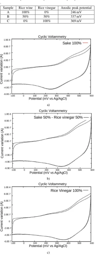
For demonstration, preliminary experiments with cyclic voltammetry has been performed with a standard electro- chemical apparatus onto commercially available rice wine (sake), rice vinegar, and a 50% mixture of both, and with
Table 3 Description of the samples and anodic peak potential for each one.
Sample Rice wine Rice vinegar Anodic peak potential
A 100% 0% 246 mV
B 50% 50% 337 mV
C 0% 100% 369 mV
Fig. 4 Results of cyclic voltammetry performed on: a) 100% wine rice (sake); b) a mixture of 50% sake and 50% rice vinegar; c) 100% vinegar.
a non-selective standard electrochemical cell (see Table 3).
The type of samples have been chosen in order to mimic a possible oxidation of wine, which turns to vinegar with time.
Fig. 5 Close-up view on the anodic peaks of the cyclic voltammetric curve of each sample. It shows clear distinct potentials confirming the idea of “voltammetric signature” of each sample.
The potential has been cyclically ramped up and down between−0.1 V and+0.6 V twice, from 0 V. A current varia- tion at the Pt working electrode has been measured between
−0.6µA and 1µA.
Figure 4 shows the results obtained for the three sam- ples. Because wine and vinegar are complex mixtures made of many compounds, the peaks are not sharp. However, it is possible to observe a wide “cathodic” peak (at positive cur- rent variation) and a wide “anodic” peak (at negative current variation).
Figure 5 shows a close-up view of the overlaid curves around the anodic peak for the three samples. And Table 3 shows the anodic peak potential measured for each sample.
A clearly distinct anodic peak potential can be ob- served for each sample: 246 mV for the rice wine; 337 mV for the 50% mixture of rice wine and rice vinegar; 369 mV for the rice vinegar. It works like if each sample can be char- acterized by its own anodic peak potential, and more gener- ally speaking by its own cyclic voltammetry curve, like a signature. The monitoring of the voltammetric signature of the samples, with a non-selective working electrode, can be a simple control of the evolution of the product.
In the example presented here, the evolution is due to an imitation of a deterioration which is oxidation of wine.
The determination of the type of evolution (standard evolu- tion, or wine fault like oxidation) is performed by the second level of control, with selective working-electrodes matrix.
7.3 Discussion about the Challenges in the Realization of the Sensor System
Such device can’t be developed without considering the problems of mutual contaminations of the sample and the sensor system, as well as the question about long-term sta- bility of electrodes and circuits. Actually, these are crucial problems as the sensor system, placed in a closed container for a long period, can’t be replaced in case of defect, without opening the container.
Such problems are a challenge to be overcome by
working in particular on the structure of the sensor system itself as well as its packaging. Redundant chemical anal- yses should be allowed, by means of high-order chemical sensors, in order to pursue reliable analyses in spite of some instabilities at the level of the electrodes.
In addition, the packaging of the system should be cre- ated in a way to avoid mutual contaminations of the sam- ple and the sensor system, and to protect the circuits. In a first instance, the protective packaging might include semi- permeable membranes at the level of the sensing parts, to avoid direct contact between the sensor system and the sam- ple to be analyzed, but still letting the chemicals of interest reach the sensing parts, through the membranes.
8. Conclusions
Chemical sensing research began with glass electrodes more than one hundred years ago, and is still expanding, going closer and closer to microelectronic devices. From the first ISFET devices in the 70’s, to the handheld gas sensing in- strument composed of arrays of integrated chemical multi- sensor systems, the research in this field spread towards al- ways more integrated and complex devices, in order to have always more generic and reliable sensors.
To take full advantage of integration, monolithic inte- gration has to be preferred to hybrid one. Actually, thanks to monolithic integration, wiring congestion is dramatically reduced giving a clear decrease of parasitic effect. Usu- ally post-processing, by making LSI first on the chip, then MEMS, is preferred.
Applications with integrated chemical sensors are very wide and depend on their operating principle. For instance potentiometric sensors are famous for the analyse of ions (like pH) for biochemical purpose. Conductometric sen- sors are more dedicated to gas sensing for environmental purpose. Capacitive sensors are typically used for humidity sensors. Voltammetric sensors have the widest range of ap- plication for liquid, and they are generally used for environ- ment, food or bio-medical purposes. And so on. However, despite their differences and their more specific areas of ap- plication, which are due mainly to their operation principle, they all have a common point. They have to be able to an- alyze always more complex mixtures. To do so, integrated sensor arrays is an inevitable development to have some on- chip intelligence for these complex data processing.
Wireless communication is another function of the de- vice which is becoming important to be integrated. Actu- ally, for some applications it is even an essential function.
In this article, we have given the example of an integrated LSI-MEMS chemical sensor for remote surveillance of the quality deterioration of some products stored on long-term inside a close container. The applications can be for instance for some beverages (wine or soft drink) or medicines stored on long-term inside a bottle. Some preliminary experiments have been described supporting the proposed analyse proce- dure.
Finally, the challenging points in the realization of the
sensor system, concerning the long-term stability as well as problems of contaminations, have been discussed. The packaging of the system as well as its structure have to be considered to overcome these problems.
There are still quite many roads to explore with inte- grated LSI-MEMS chemical sensors, making it an expand- ing field of research, for which new applications can still be found.
References
[1] A. Hierlemann and and H. Baltes, “CMOS-based chemical mi- crosensors,” Analyst, vol.128, pp.15–28, 2003.
[2] A. Hierlemann, O. Brand, C. Hagleitner, and H. Baltes, “Micro- fabrication techniques for chemical/biosensors,” Proc. IEEE, vol.91, no.6, pp.839–863, 2003.
[3] S. Joo and R.B. Brown, “Chemical sensors with integrated electron- ics,” Chem. Rev., vol.108, no.2, pp.638–651, 2008.
[4] Y. Vlasov and A. Legin, “Non-selective chemical sensors in analyti- cal chemistry: From electronic nose to electronic tongue,” Fresenius J. Anal. Chem., vol.361, pp.255–260, 1998.
[5] P. Bergveld, “Development of an ion-sensitive solid-state device for neurophysiological measurements,” IEEE Trans. Biomed. Eng., vol.BME-17, no.1, pp.7071, 1970.
[6] P. Bergveld, “Development, operation, and application of the ion- sensitive field-effect transistor as a tool for electrophysiology,” IEEE Trans. Biomed. Eng., vol.BME-19, no.5, pp.342–351, 1972.
[7] A. Hierlemann, Integrated Chemical Microsensor Systems in CMOS Technology, Springer, 2005.
[8] C.C. Johnson, D. Moss, and J. Janata, “Selective chemical sensitive FET transducers,” US Patent no.4020830, 1970.
[9] http://ci.nii.ac.jp/naid/110002518294 (japanese)
[10] J. Janata, Principles of Chemical Sensors, Springer Publisher, 2nd ed., 2009.
[11] Z.H. Lin, K.S Booksh, L.W. Burgess, and B.R. Kowalski, “A second-order fiber optic heavy metal sensor employing second-order tensorial calibration,” Anal. Chem., vol.66, no.15, pp.2552–2560, 1994.
[12] R.G. Brereton, MultiVariate Pattern Recognition in Chemometrics, Elsevier Science: Amsterdam, The Netherlands, 1992.
[13] U. Weimar and W. G¨opel, “Chemical imaging: II. Trends in prac- tical multiparameter sensor systems,” Sens. Act. B, vol.52, no.1-2, pp.143–161, 1998.
[14] A. Heilig, N. Barsan, U. Weimar, M. Schweizer-Berberich, J.W.
Gardner, and W. G¨opel, “Gas identification by modulating tempera- tures of SnO2-based thick film sensors,” Sens. Act. B, vol.43, no.1-3, pp.45–51, 1997.
[15] T. Takada, “Temperature drop of semiconductor gas sensor when exposed to reducing gases — Simultaneous measurement of changes in sensor temperature and in resistance,” Sens. Act. B, vol.66, no.1- 3, pp.1–3, 2000.
[16] K. Persaud and G. Dodd, “Analysis of discrimination mechanisms in the mammalian olfactory system using a model nose,” Nature, vol.299, pp.352–355, 1982.
[17] A. Hierlemann, O. Brand, C. Hagleitner, and H. Baltes, “Micro- fabrication techniques for chemical/biosensors,” Proc. IEEE, vol.91, no.6, pp.839–863, June 2003.
[18] D.F. Lemmerhirt and K.D. Wise, “Chip-scale integration of data- gathering microsystems,” Proc. IEEE, vol.94, no.6, pp.1138–1159, June 2006.
[19] O. Brand, “Microsensor integration into systems-on-chip,” Proc.
IEEE, vol.94, no.6, pp.1160–1176, June 2006.
[20] T. Hizawa, K. Sawada, H. Takao, and M. Ishida, “Fabrication of a two-dimensional pH image sensor using a charge transfer tech- nique,” Sens. Act. B, vol.117, no.2, pp.509–515, 2006.
[21] K. Sawada, T. Shimada, T. Ohshina, H. Takao, and M. Ishida,
“Highly sensitive ion sensors using charge transfer technique,” Sens.
Act. B, vol.98, no.1, pp.69–72, 2004.
[22] M.Y. Afridi, J.S. Suehle, M.E. Zaghloul, D.W. Berning, A.R.
Hefner, R.E. Cavicchi, S. Semancik, C.B. Montgomery, and C.J.
Taylor, “A monolithic CMOS microhotplate-based gas sensor sys- tem,” IEEE Sens. J., vol.2, no.6, pp.644–655, 2002.
[23] M. Zimmermann, T. Volden, K.-U. Kirstein, S. Hafizovic, J.
Lichtenberg, O. Brand, and A. Hierlemann, “A CMOS-based integrated-system architecture for a static cantilever array,” Sens.
Act. B, vol.131, no.1, pp.254–264, 2008.
[24] A.M. Kummer and A. Hierlemann, “Configurable electrodes for capacitive-type sensors and chemical sensors,” IEEE Sens. J., vol.6, no.1, pp.3–10, 2006.
[25] S.M. Martin, F.H. Gebara, B.J. Larivee, and R.B. Brown, “A CMOS- integrated microinstrument for trace detection of heavy metals,”
IEEE J. Solid-State Circuits, vol.40, no.12, pp.2777–2786, 2005.
[26] M. Schienle, C. Paulus, A. Frey, F. Hofmann, B. Holzapfl, P.
Schindler-Bauer, and R. Thewes, “A fully electronic DNA sensor with 128 positions and in-pixel A/D conversion,” IEEE J. Solid-State Circuits, vol.39, no.12, pp.2438–2445, 2004.
[27] T. Yamazaki, T. Ikeda, M. Futagawa, F. Dasai, M. Ishida, and K.
Sawada, “An electrochemical array sensor with CMOS signal pro- cessing circuits integrated on a single chip,” Proc. IEEE Biomedical Circuits and Systems Conference 2010 (IEEE BioCAS 2010), Pa- phos, Cyprus, pp.138–141, 3-5 Nov. 2010.
[28] R.A. Yotter and D.M. Wilson, “A review of photodetectors for sens- ing light-emitting reporters in biological systems,” IEEE Sens. J., vol.3, no.3, pp.288–303, 2003.
[29] V.P. Iordanov, B.P. Iliev, A. Bossche, J. Bastemeijer, P.M. Sarro, I.T.
Young, G.W.K. van Dedem, and M.J. Vellekoop, “Integrated sensor arrays for bioluminescence and fluorescence bio-chemical analysis,”
Proc. IEEE Sensors, vol.2, pp.810–813, Vienna, Austria, Oct. 2004.
[30] H. Eltoukhy, K. Salama, and A. El Gamal, “A 0.18-µm CMOS bi- oluminescence detection lab-on-chip,” IEEE J. Solid-State Circuits, vol.43, no.3, pp.651–662, 2006.
[31] Z.J. Davis, G. Abadal, B. Helbo, O. Hansen, F. Campabadal, F.
Perez-Murano, J. Esteve, E. Figueras, J. Verd, N. Barniol, and A.
Boisen, “Monolithic integration of mass sensing nano-cantilevers with CMOS circuitry,” Sens. Act. A, vol.105, no.3, pp.311–319, 2003.
[32] C. Vancura, M. R¨uegg, Y. Li, C. Hagleitner, and A. Hierlemann,
“Magnetically actuated complementary metal oxide semiconductor resonant cantilever gas sensor systems,” Anal. Chem., vol.77, no.9, pp.2690–2699, 2005.
[33] K. Sawada, T. Ohshina, T. Hizawa, H. Takao, and M. Ishida,
“A novel fused sensor for photo- and ion-sensing,” Sens. Act. B, vol.106, no.2, pp.614–618, 2005.
[34] Y. Li, C. Vancura, D. Barrettino, M. Graf, C. Hagleitner, A.
Kummer, M. Zimmermann, K.U. Kirstein, and A. Hierlemann,
“Monolithic CMOS multi-transducer gas sensor microsystem for or- ganic and inorganic analytes,” Sens. Act. B, vol.126, no.2, pp.431–
440, 2007.
[35] C. Hagleitner, A. Hierlemann, O. Brand, and H. Baltes, “CMOS single chip gas detection systems — Part I,” Sensors Update, vol.11, no.1, pp.101–155, 2002.
[36] K.-S. Yun, J. Gil, J. Kim, H.-J. Kim, K. Kim, D. Park, M. su Kim, H. Shin, K. Lee, J. Kwak, and E. Yoon, “A miniaturized low-power wireless remote environmental monitoring system based on electro- chemical analysis,” Sens. Act. B, vol.102, no.1, pp.27–34, 2004.
[37] A. Tixier-Mita, T. Takahashi, and H. Toshiyoshi, “A proposal on surveyance of substances in unopened bottles by integrated wire- less chemical sensors array,” Proc. 28th SENSOR SYMPOSIUM on Sensors, Micromachines and Application Systems, Tokyo, Japan, 26-27 Sept. 2011.
[38] P.T. Kissinger and W.R. Heineman, “Cyclic voltammetry,” J. Chem.
Educ., vol.60, no.9, pp.702–706, 1983.
Agn`es Tixier-Mita received her Mas- ter in Material Sciences at the Ecole Nationale Sup´erieure d’Ing´enieurs - ENSI de Caen, Caen, France and her Ph.D. Degrees in Electrical En- gineering from the University of Lille I, Lille, France, in 1994 and 1998, respectively. From 1999 to 2001, she joined as a post-doc the Lab- oratory for Integrated Micro-Mechatronic Sys- tems (LIMMS/CNRS) - Institute of Industrial Science (IIS), UMI 2820, The University of To- kyo, Tokyo, Japan. Between 2001 and 2007, she became successively an Assistant Professor at the IIS, then a research en- gineer of CNRS at the LIMMS/CNRS-IIS UNMI 2820. From 2010, she became an Associate Professor with the Center for International Research on Micro & Nano Mechatronics (CIRMM) at IIS. Finally from June 2010 she has a double post as an Associate Professor with Research Center for Advanced Science and Technology (RCAST), The University of Tokyo.
Her research interests include integration of chemical sensors with LSI, as well as wireless sensors.
Takuya Takahashi received the B.E. degree from the Tokyo University of Science, Tokyo, Japan, in 2002. Since April 2002, he has been a Technical Staff with the Institute of Indus- trial Science, The University of Tokyo, Tokyo, Japan. His research interests include microma- chining in both bulk silicon and plated metals.
He has been engaged in R&D of optical MEMS spectrometers for astronomical applications and integrated MEMS.
Hiroshi Toshiyoshi received M.Eng. and Ph.D. Degrees in Electrical Engineering from The University of Tokyo, Tokyo, Japan, in 1993 and 1996, respectively. In 1996, he joined as a faculty member with the Institute of Indus- trial Science (IIS), The University of Tokyo.
From 2009, he has been a Professor with Cen- ter for International Research on Micro & Nano Mechatronics (CIRMM) at IIS. During this pe- riod, from 1999 to 2001, he was a Visiting As- sistant Professor at University of California Los Angeles. From 2002 to 2007, he was a Co-Director of LIMMS/CNRS-IIS UMI-2820, which is an international joint laboratory of Centre National de la Recherche Scientifique (CNRS) France. From 2005 to 2008, he has been a project leader of the Optomechatronics Project at Kanagawa Academy of Science & Technology (KAST). Since May 2009, he has a double post as a Professor with Research Center for Advanced Science and Technology (RCAST), The University of Tokyo. His research interests include optical and radio-frequency application of MEMS.