Composition analysis of strongly oxidized
Nb_3Ge with X.P.S.
著者
OGUSHI Tetsuya, OSONO Yoshihisa, NUMATA
Tadashi
journal or
publication title
鹿児島大学工学部研究報告
volume
28
page range
185-197
別言語のタイトル
強く酸化されたNb_3GeのX.P.S.による組成分析
URL
http://hdl.handle.net/10232/11400
Composition analysis of strongly oxidized
Nb_3Ge with X.P.S.
著者
OGUSHI Tetsuya, OSONO Yoshihisa, NUMATA
Tadashi
journal or
publication title
鹿児島大学工学部研究報告
volume
28
page range
185-197
別言語のタイトル
強く酸化されたNb_3GeのX.P.S.による組成分析
URL
http://hdl.handle.net/10232/00004567
COMPOSITION ANALYSIS OF STRONGLY OXIDIZED Nb3Ge
WITH X. P. S.
Tetsuya OGUSHI, Yoshihisa OSONO and Tadashi NUMATA
( Received May 31, 1986 )ABSTRACT
A new candidatite for superconductor is introduced as the results of our recent studies on the
fabrication and properties of a strongly oxidized Nb3Ge thin film prepared on a AI2O3—substrate.
These experiments were triggered by our investigation to improve the reproducibility of the resist
ance anomaly of Nb—Si thin films reprorted earlier by us.The new films are confirmed to have resistance transition at a temperature of 44.5K along with a
large diamagnetic transition. They also has good reproducibility and stability. A substantial amount of
Al and 0 exisis in the film resulting in the formation of ND2O5, Ge02 and AI2O3 through strong oxida tion. The chief characteristics of this transition are notably similar to superconductors with phonon— mediated electron-electron interaction. To explain the high Tc, however, we might have to consideranother mechanism (i. e excitonic mechanism), which acknowledge the possibility of high—temperature
carrier pairing.1. INTRODUCTION
The pursuit for material with high superconducting critical temperature has been an area of in
tense research. In 1973 Gavalar1} sputtered Nb-Ge films in high Argon pressure onto hot substrates
and obtained superconducting transitions with an onset temperature (Tco) of 22.3K. Soon after,
Testardi2) achieved TCo = 23.2K using the same material. Many researchers have extensively ex
amined Nb3Ge . The TCo for this compound has not exceeded 23.9K3) until now.
Dew-Hughes4 predicted from the empirical relationship for the critical temperature of some A15
superconductors, that if Nb3Si crystallizes in the A15 structure, it should have Tc —38K. However,
crystal in a good ordered state with a small lattice constant is very difficult to make. Geller
also has
suggested a stoichiometric P -W type Nb3Si should have a superconducting transition temperature
between 31K and 35K. Many experimental6 ~16) have been attempted to obtain a smaller lattice con
stant of —5.09A with A15 phase to achieve a high Tc. Although the lattice constant and phase were
realized, the Tc for Nb3Si never exceeded 18.6K.Recently, many theories have been proposed for a high temperature superconductor from elec
tron-electron interaction via exchange of nonphonon17 ~ 21) . In particular, Allender, Bray and
Bardeen18) have discussed in detail the possibility of using a narrow-gap semfconductor as a suitable
medium for an exciton mechanism superconductor. In their theory they discussed the possibility ofex-Note added for proof
186
mRm±^T^^mftn^
H 28 •*§- (1986)
citon mechanism and phonon mechanism working together. It seems quite interesting from an ex perimental point of view because superconductors from phonon—mediated electron—electron interac tion such as Nb3Si and Nb3Ge could be converted to that state with both the exciton mechanism and the phonon mechanism.
One of the authors of this manuscript has reported a resistance anomaly of very thin Nb—Si
film
. The anomaly is marked by a sudden drop in the resistance by a factor of ~103 at a tempera
ture of ~ 180K. This behavior bears many resemblances to that of a superconductor. However, the accuracy of measurements had been hampered by poor reproducibility of the anomaly. Recently, it be came apparent to us that the presence of oxygen during sputtering remarkably improved the repro ducibility of the resistance anomaly and therefore promoted the oxidation of Nb3Ge where Ge is sub stituted for Si in the Nb-Si film.Artificially oxidized films were examined, but the characteristics underwent changes every hour
and were also affected by thermal cycles. Therefore, Nb3Ge films with Tco~21 —22K prepared
one-four years ago and thus, naturaly oxidized in air , have been examined.In this paper we will demonstrate, as testimony for their candidacy for superconductor, the resis
tive transition and diamagnetic behavior of the Nb3Ge films oxidized naturaly. Results of X-ray and
the data from X—ray photoelectron spectroscopy analysis (X.P.S) are also presented.
The mechanism of this superconductor has not yet been clarified. However, it has emphatically
different characteristics from "an ordinary superconductor". For example, light sensitivity, X—ray
irradiation-sensitivity and large hysteresis (~9K in maximum) between a cooling and warming pro
cess have been observed. These phenomena would not be explained by a phonon—mechanism—supercon
ductivity.II. EXPERIMENTS
A. Sample Preparation
Sample were prepared by the following methods:
[1] Nb and Ge were sputtered onto a heated substrate in highly pure Ar with a controlled slow of ox
ygen into the chamber.[2]After preparing Nb3Ge with high Tc by a sputtering process, they were oxidized in a pure oxygen
atmosphere.[3) Nb3Ge was naturally oxidized in air for 1~4 years.
The samples obtained by the first two methods showed a lack of stability, and characteristics
changed with time. The results obtained by these two methods will be published elsewhere.
All samples reported here were prepared by method [3] where the D.C. high—rate sputtering car
ried out in a can cooled by liquid N2. All films were deposited onto polished single—crystal sapphire
substrates 15X10X 1.0mm in size. The thickness of the films were 3000A~5000A. The details have
been described by Ogushi et al .B. Method of Measurement
The transition temperature was measured by using an Au—0.07%Fe versus chromel thermocouple
calibrated with GaAs diode standard (Lake shore Corp.) and with the boiling temperature of liquid N2
and He. The thermocouple was held tightly to the samples. A digital voltmeter was used to read thevoltage of the thermocouple with an accuracy of five digits. Periodically to confirm the accuracy of
our measurements the samples were cooled or warmed very carefully and slowly at the rate of IK/Composition Analysis of Strongly Oxidized Nb3Ge with X. P. S. 187
min. A metal Dewar with a dark interior for liquid—He was used to cool samples. Periodically, a glass Dewar was used instead to introduce light.
The inductive measurements were carried out with a helical coil followed by a pick up coil of the same type which was in direct contact with the sample to measured. Duplicate pairs of coils were util ized to prevent sprious signal detection. Normally, the frequency of the driving coil was 88C/sec with frequent changes from 88C/sec to IOC/sec. To observe the effect of eddy current, a pure Nb foil with much higher conductivity than the films were examined for all frequency used here. However, no sig nal except those attributed to the real superconductive transition was detected.
The magnetic field—strength of the driving coil was purposely chosen to be low as not to induce vortex penetration through a thin film. The signal from the Nb foil was then used for calibration of absolute values and sighns of susceptibility.
C. Transition Measurement
A quasi four—terminal—method in which pure gold wires are contacted with pressure to films was used. These measurements were verified at intervals by the use of typical four terminal method to in sure uniformity of current necessary for accurate measurements. Both methods were sound to coin cide. The measuring current was normally lQjuA but sometimes 20/iA was used to observe current dependency.
Fig. 1 shows a photocopy of X—Y recorder trace of a resistive transition curve for the sample
X-457. The dotted line represents the diamagnetic susceptibility ( X ) which was transcribed from a
X-Y recorder trace. The TCo of the transition of this film is 44.5K which was the highest detected inour experiments. The diamagnetic trace increases towards a plus porality maximum of 0.4, crossing
the absissa and goes toward the minimum of X = —0.92. The diamagnetism trace decrease inversely with the resistance. The temperature at which the resistance reaches it's half value (Tc) is 34.0K. But5 # 4 - R
-x ;
_;
-£3
• _ CC 2 -K
-1 -•• * -r \ 1 •••• i i i 1.0 0.8 X 1 ? 0.6(/) H LU 0.4 2CD < 2 0.2 < Q 70 50 30 10Temperature T(K)
Fig. 1 Resistive transistion curve (solid line) and
the accompanied diamagnetic susceptibility
(X) for sample X for sample X 457.Tco =
44.5K and X = — 0.92 at the maximum (in the cooling course).
1.0 0.8 _ X I 0.6 ^ co f-0.4 w CD < 5 4 R -x i J £ 3
\
/ 2U^^Mi^A alvAiii MiAAl"\ ,
1
1 IK yviiWjyfV VMTV^ jfi?\1 0 , 1 - 0.2 < 100 70 50 T [KJ 30 10Fig. 2 Same trace in the cooling course for sam ple YH 8001-16 as in Fig. 1 (Tco = 30.5,
Tc = 30.0, Tce = 29.5K). Tce represents a
188 ^ ^ - x ^ x ^ ^ m f t m^ m 28 •# (1986)
the resistance remains finite until 7.5K.
In Fig. 2, a sharp transition for sample YH 8001—16 is demonstrated. The transition temperature are Tco~30.5K, Tc — 29.5K and Tce = 29.5K. The Tce is the temperature at which a resistance be comes zero. Unexpectedly, the trace declined to minus resistance in most samples particularly in those with the sharp transition. This is ascribed to a complex electromotive force (EMF), the amplitude of which is partly dependent on temperature and is quite noisy;
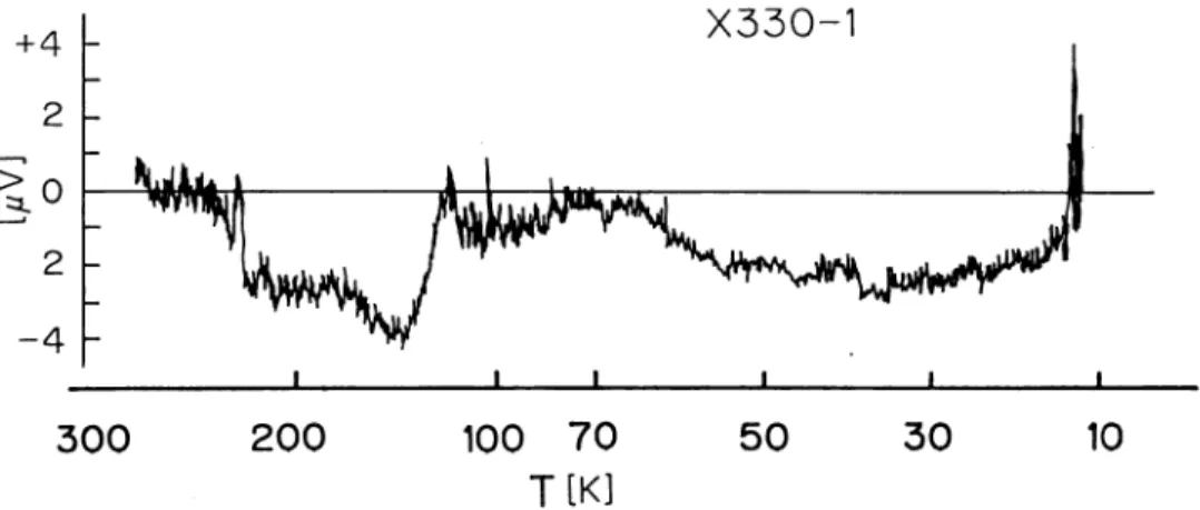
The typical EMF and temperature for sample X 330— II is shown in Fig.3. It attains maximum
300 200
100
70
TIK]
X330-1
50 30 10
Fig. 3 Typical "zero bias voltage" induced between terminals for a measurement of a resistance. This
voltage is super imposed on an ordinary R—T curve. A noisy trace of R is due to voltage. A
polarity of this voltage usualy changes from ( —) to ( + ) polarity below Tce. This leads to a false residual resistance (in the course of cooling).
Table 1
Sample No.
T (REDUCTION) (K)
Ton Tc Tce Ton
T (RAISE) (K) Tc Tce X 457 44.15 34.0 7.5 22.0 12.5 7.5 Y H 8001-16 30. f) 30.0 29.5 25.0 24.0 22.5 X 279 37.0 36.0 33.5 24.5 23.5 21.2 X 277 32.5 32.0 30.0 26.0 24.0 20.0 ( * ) X 2770 39. n 36.5 9.5 24.5 22.5 9.5 X 100 35.0 34.0 - 26.0 24.5 15.0 X 308 34.0 32.5 30.5 25.0 21.9 20.0 ( * ) X 309 25.1 7.5 - 18.5 8.4 -X 324- 29.5 26.8 - 21.4 17.1 -X 326 33.0 32.8 23.5 23.5 23.9 12.8 X 280 31.2 29.3 25.0 23.79 20.1 19.5 X 310 34.8 31.6 29.8 25.6 21.5 20.1 X 332- I 33. r> 33.0 - 24.5 24.6 19.0 X 330- 1 I 32.3 30.4 29.2 21.3 19.0 -X 330 33.1 32.4 32.3 24.3 22.6 20.0 X 331 37. f) 37.5 37.5 25.0 23.0 21.0 ( it) X 331 37. 5 37.5 37.5 37.5 37.5 37.5
Composition Analysis of Strongly Oxidized Nb3Ge with X. P. S. 189
and minimum ( + ) A/J.V. When this EMF signal is superimposed on an ordinary R—T curve, the results is an R—T curve similar to that shown in Fig. 2. This addition signal can not be ignored because the measuring currents of film resistance is usually IOjuA, which induces, for example, 40juV between voltage terminals of a sample with 4 H in the resistance. The noisy characteristic of R—T curve is, therefore, presumably due to this EMF.
In Table I, Tco> Tc and Tce in both the cooling and warming processes are listed. The hysteresis
is described below.D. Hysteresis
Plots of a resistance vs the temperature have a hysteresis loop for the thermal—cycle. This hys teresis is not so simple. The distortions in shape of the hysteresis loop are determined by the starting temperature of cooling and warming a sample in the thermal—cycle.
The traces of resistive transition together with the diamagnetic in which the sample X 280 was cooled from room temperature is shown in Fig. 4. The minor hysteresis loops for the same samples are shown in Fig. 5. The trace with numbered 1 was cooled from 77K to 22.5K and then warmed up to 34.0K (No.r). The trace (No.2,2') is for the thermal cycle from 34.0K down to 13.6K and then from 13.6K up to 28.0K. The trace (No,3,3') represents a similar thermal cycle 28.0K down to 5.0K and then from 5K the temperature was raised.
The quantitative analysis was carried out on sample X 332 (Fig. 6) having the largest observed hysteresis in this study. The results are plotted on semilog graph paper in Fig. 7. The dashed line represents Tco obtained in the cooling process of the film from room temperature. The solid line sig nifies Tco in the process of warming the sample immediately after cooling the sample always from a room temperature to various T on a horizontal— coordinate axis. The difference between the two lines represents the hysteresis at a corresponding temperature. The linear dependence of InTco on T in the warming process is quite implicating.
Fig. 4 R—T and the diamagnetism for sample X 280 is shown. The temperature of the sam ple was decreased from a room tempera
ture. This is shown to the help an explana tion of a characteristics in thermal cycles.
5 X-280 -4 CT~*u^
53
or • Pi r 1* 2 1km3
H 66 54 43 31rT2o5
P 5 T [K]Fig. 5 Minor hysteresis for thermal cycles. Tran
sition temperatures in the course of cool
ing or warming change depending on what
temperature is the starts of thermal cycles.
190 I I * ? I ¥ S I » S I S Kt 28 ^f (1986) 1 1 1— X-332 V ^ U i S
!«
' y£ -AT — — ^ — I K "U*
ltd
1.0 -2 0.8 CO t -LiJ 0 6 -z. <JJ < 0.4 > < n 0.2 0 77 66 54 43 31 T[K] 20 4.2Fig. 6 Quantitative analysis of the hysteresis was carried out for the sample X 332.
100 : #332
cooling
warmig
logTco=0.4T+log22 10 20 TtK] 30Fig. 7 Temperature dependence of hysteresis loops for the sam ple X 332. The sample was cooled exactly from room temperature. The transition temperature is represented by a dashed curve. A curve labeled (♦) shows Tco in the course of warming but for the temperature T until which the sample was cooled from a room temperature. The cri tical temperatures for as deposited Nb3Ge were Tco=22.1, Tc=21.3 and Tce=16.3X.
E. X—rav Diffraction Results
Fig. 8 shows the X-ray scan for sample X 277, with a transition temperature of 39.0K. Eight
A15 peaks were observed up to 2 6 =90°.
These peaks gives a lattice constant (ao) of 5.124A. This lattice constant is less than the smallest
a0 = 5.13A reported for deposited Nb3Ge films. This scan is characteristic of samples studied in this
report. The scan for sample X 309 is so sharp than it shows definite KQi~ Ka2 splitting. The both
lattice—constants obtained from K«i and K<*2 concide with ao = 5.110A. As is shown later, these films
contain a large amount of Al. An unsolved problem is what kind of matrix results in such small lattice constant and good ordered state as will be discussed later.Composition Analysis of Strongly Oxidized Nb3Ge with X. P. S. 191 20 1 T I" Sample No. 277 200 1 < 1 210 Tc=39.0K >- ao=5.125A co z LU z 110
\J
211WJL
I i L. • i i i 30 40 ANGLE 20c 50 60Fig. 8 X—ray trace for sample X 277.
100 80 60 40 20 0 Fig. 9 -1 r — \ -• Ois • v-~.^
-^yy*[2p Ge3P
_.!__ 60 120 DEPTH [A] 180XPS-depth profile for a sample X-10-B with high critical temperature.
1 1 r Sample No. 277 i i Tc = 39.0K ao=5.125A 320
h321
.1 i 1_ 400 L-421 i 1. 70 80 ANGLE 20° 90 u u 80 i i • 60 Nb3d -40 ?0r-
--/
Ois""aSTT
_ y Ge3p " • i i 1 1 200 700 1200 1700 2200 2700 3200 DEPTH [A]Fig. 10 XPS-depth profile. The film thickness was 3200A
(a) Composition analysis
X—ray photoelectron Spectroscopy (XPS or ESCA) is a very powerful tool in the study of bind ing energy of core electron in atoms and molecules. The chemical shifts (A Eb) of an individual ele
ment have been correlated with the it's binding state in various compounds.
The composition analysis was carried out by XPS. A depth profile (Fig. 9) of a sample X—10—E shows the existence of large quantity of Oxygen ( —85% at the surface), Nb, Al and Ge which are in
the form Nb205, Nb20, NbO,Al203 and Ge02 to the depth of 50A, identified by the oxide shifts for the
various elements24~27). Even at the depth 50A~200A, the chemical shift from the base metals by ox
idation are still observed. The carbon contamination signal was used for the charge—up—compensation.
The binding energy of a pure Nb was estimated, and was in good agreement with that obtained by
Karulkar et al24). and a measurement of a Nb with four—nine—purity. The standard for Al are from
Ref. 28.
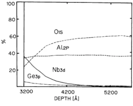
Fig. 10 is depth profiles between 200A and 3200A. and Fig. 10 is that between 3200A and
5700A. These profiles are markedly different from of deposited NbsGe
since about 30%Al2p and
18%Ois are contained in the main part (200A —3200A) of the film. As mentioned before, the film
thickness is 3200A, estimated from multiple—beam interferometry. The distribution of Ois seems to
192 j f l a ^ ^ . T ^ a S f l f ^ g g ^ 28 -§• (1986)
(Fig. 9 and 10). This shows that Oxygen has diffused into the film from the surface. It is well know that oxide layer of Nb or Al work as a protective stable layer against the progress of oxidization of metals.
The large amount of Oxygen in films studied in the present research is caused, in our conjecture, by a channel formed by a poorly defined oxides because of the existence of complex elements such as
Nb, Ge and Al.
On the other hand, the mechanism proposed by Ihara et al2
to explain the enrichment of Nb
atoms in surface region of NbsGe may also explain the uniform distribution of Al in the region of 200A-3200A.The Nb—Ge atomic ratio increases to 5.5 from 3.0 which was estimated from as—deposited NbsGe
by peak—intensity ratio of the Nbsj to Ge3p. This ratio will be represented by
NbsGei-x-It is impossible to determined, at the present stage of our studies, which additional elements con tribute to the A15 structure and very small lattice—constant as determined by X—ray analysis.
Fig. 11 shows that a large amount of Nb3d has diffused into the sapphire substrate up to ~4700A
through the interface between the film and the sapphire substrate. On the contrary, the peak intensityof Al including Al2p and Al2s evidently decrease [Fig. 14 and 15 (b)]. This means that a exchange diffu
sion of Nb and Al has occurred on both sides of the interface. The Al librated from Al203, in our3200 4200 5200
DEPTH [A]
Fig. 11 XPS-depth profile.
opinion, is the source of Al contained in the films. This pattern of compositions—distribution can easi ly be imagined to depend on the orientation of the sapphire surface.
In our experiment, a surface of a sapphire which makes an angle of 90 + 7°C to C axis is used as the substrate. This results in a facilitated reaction at the interface..
The reaction of Nb alloy with Al203 has discussed more extensively Schmid et al. . They pre pared ND3AI with a transition temperature >17K by sputtering Nb onto a hot substrate. Nb metal re duces the Al203 released Al through the formation of ND3AI despite Nb's lower Oxygen affinity than Al. The Rutherford back scattering results indicate a fairly uniform Al concentration throughout the film. This seems to coincide with our results,
(b) Binding state
Fig.12 (a) shows the binding energy spectrum of Nbsa of NbsGe. The binding energy of Nb—3ds/2 peak and Nb—3d3/2 peak are 200.8eV and 203.6eV respectively, after charge up compensation, be
tween the film thickness 400A and 3200A. Thses values are lower by 1.5eV than that obtained by
Composition Analysis of Strongly Oxidized Nb.iGe with X. P. S. 193 •< Q_ LU Q 210 200
BINGING ENERGY (eV)
(a) Nb-3d XPS spectra taken from sam ple X-10-B.
(b)
Fig. 12
210 200
BINGING ENERGY (eV)
Nb-3d XPS spectra at the depth between 3200A and 5250A.Ihara et al. from a stoichiometric Nb3Ge25). This suggests together with the composition ratio, that
the films studied in this report are not simple Nb3Ge. Another possibility is the formation of ND3AI
or Nbs(Ali-xGex) as a part of a film.
The results on Nbsd are summarized in Fig. 13. The chemical shifts near the surface (0 —300A)
show the exsistence of Nb205, Nb02 and NbO. The binding energies Nb-3d5/2 and Nb-3d3/2 are con
stant from 300A to the depth ~3200A which corresponds to the film thickness. AEB~0.3eV of bind
ing energy of Nb—3d3/2 appear at the interface where a reaction with the substrate is expected.
XPS spectra for Ge—3d is shown in Fig. 14. The corresponding binding energy is 121.0eV which
matches the results of Ge—3p. .
Fig. 15 is that for Al—2p. The observed binding energy is —76.5eV in the core of the film. This
also shifts toward a greater binding energy by 1.5eV at the interface reaching that of a sapphire
(78.0eV). A calibration for a charge—up has not been done in a sapphire substrate which results in the
large
AEb-The observed value Al—2p is higher than that of pure Al suggesting that Al has made a compound with another element. A large amount of Al has been found in the film as demonstrated in Fig. 10
194 K g b ± ¥ X ¥ t $ f f l f t m ^ 28 -§• (1986)
Nb3d
<i
500 h 1000 •< 1500X
2000
^ 2500
LU 3000 Q 3450 4450 5450 (11) -© (2-1) (1-2) ©♦!► 0 (2-2) (3)®X-10-B.5/2-Bx-10-B.3/2
^Nb205.3/2 "
$ Nb20st5/2 ♦Nbstd.5/2
• Nbstd.3/2201 202 203 204 205 206 207 208 209
BINGING ENERGY [eV]
Fig. 13 The result obtained in Fig. 12 are summarized.
130
120
110
100
BINGING ENERGY (eV)
Fig. 14 Ge—3p XPS spectra taken from sample
X-IO-B. o o
Al2p/V^
CNJ_Ju\^.
o ^yH/\\\ oy//\\\ ^ ^ ~
oA
•<//a\v—
o Xypt—-—
o H//AW
o u .y i\c—-^~~~
Cvi LU4t—
ojflf—,
o// w
o_-// \v
,—.
roJ. v___
80 70 O O <\J ro O O CvJ o o CvJ LOBINDING ENERGY (eV) BINDING ENERGY (eV)
Composition Analysis of Strongly Oxidized Nb.sGe with X. P. S. 195
Ge) the homogenous niobium chain of which is shorter than ND3AI , there still remains a surplus of Al.
Aside from problems oxides in the film were examined because ~18% Oxygen had been detected (Fig. 10). The results from the XPS spectra of Nb, Ge and Al can not verify the existence of the ox ides of each metal.
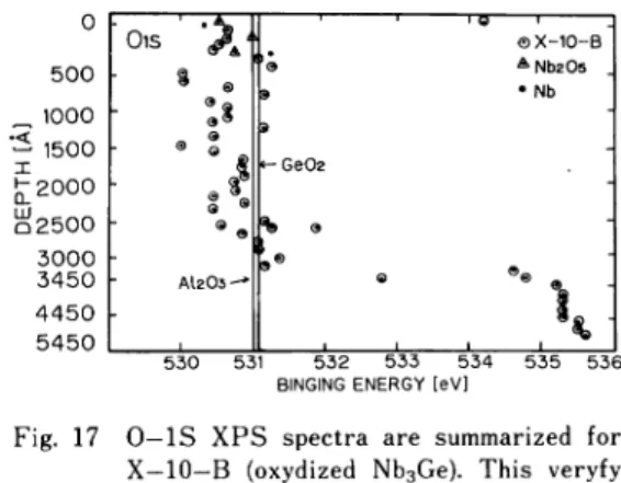
Therefore, the XPS spectra of Ois was investigated. The results are shown in Fig.17. Vertical lines with marks AI2O3 and Ge02 indicate binding eoergies of Ois in AI2O3 and Ge02. Symbols (A)and
(O) represent the measurements of standard ND2O5 and SiO. Symbol (O) denotes the experimental.
These data have poven the existence of oxides such as AI2O3, AI2OX. Ge02 and ND2O5 even in the matrix of A15 phase or in the grain boundary of the film.
0 1 — 1 1— 1 Al2p x-10-B 500 - ---» 1000 : . • < • . -j2 1500 ;
-0^2000
- • • -LJJ • Q2500 ~ • 3000 - -3450 ~ • . 4450 : 5450 - 1 » i— 1 • 74 75 76 77 78BINGING ENERGY [eV]
Fig. 16 The results from Fig. 15 are summarized.
0 "01S
^
• 9 1 ©X-10-B 500 . •w .© 99 A Nb205• Nb „ 1000 - U -— 1500 . 9 » * _ X t » fr-Ge02 £2000 - " a 2500 9 ©% 9 -3000L-
-3450 AI2O3 -* 9 1 1 4450 5450 _j , 530 531 532 533 534 535 536BINGING ENERGY [eV]
Fig. 17 0—IS XPS spectra are summarized for X-IO-B (oxydized Nb3Ge). This veryfy that the existence of complex oxide such as A1203, Ge02, Nb205 in the matrix or in grain boundary of the film.
III. DISCUSSION
We consider the transition reported here a superconductive one due to the associated large di-amagnetism and a current—induced—transition by ~2X10~ A at 4.2K (not mentioned in this report).
It has became clear that a NbsGe , which contains a large amount of Oxygen results in the forma tion of oxides such as Nb2Os, Nb02, Ge02, AI2O3 and AI2OX leading to a susptantially enhanced tran sition temperature. The better the qualities the deposited NbsGe has, the higher the Tco and the sharper the transition it will bring about, after oxidation. In our experiments, NbsGe with Tco less than 19K has not shown any increased transition —temperatures. Our results demonstrate that this spectracular jump of superconductive transition temperature are undoubtedly related to the mechan ism of an ordinary superconductor.
The A15 strcture, however, even with the ao~ 5.125 or 5.110A obtained by us, could not have a Tco as high as 44.5K. Furthermore, the superconducting characteristics are remarkably different from that of an ordinary superconductor. The first example is the existence of a large hysteresis loop in a resistive transition—characteristic caused by thermal cycles. The typical one for sample X332 is shown in Fig. 6. As is explained in II —D, the transition temperatures Tco s in warming process de pend on the lowest end of temperature in the thermal cycles, the higher returning—temperatures of the cycles were fixed always to a room temperature. The horizontal coordinate axis shows the lowest
196
m ft & ±¥ :l ¥ $>ffl ft m %
m 28 ^ (me)
end of temperature in the cycles. The vertical axis indicate correlative TCo to the lowest tempera
tures (returning ones) in the warming process. In this same manner, the solid line in Fig. 7 was plot
ted. The TCo obtained in cooling process exactly from a room temperature is shown by a dashed line.
The solid line is represented by log TCo= 0.4T + log22 below 19K. We think that the enhancement of
the critical temperature ( « ) discussed by another mechanism (such as excitonic mechanism) which de
pends on temperature and has a slope of 0.4T on as shown in Fig. 7. 22K is the critical temprature of
an ordinary superconductor. « staturates at the temperature 19K results in a disappearance of the hysteresis. We note in parenthesis that Tco oi as deposited thin film was 22.IK in good agreement with Tco at T = 0 in the above equation.A second example is sensitivity to light. The hysteresis was observed only when the measurement was carried out in a metal Dewar which has a dark interior. The hysteresis disappeared in a transpa rent glass Dewar.
The third evidence is that the R in R—T curve is very noisy. The very noisy zero—bias voltage such as shown in Fig. 3 is superimposed on an ordinary one. The voltage mainly is due to thermoelec tricity. A small amount of noise, however, is thought to be caused by piezoelectricity induced by a strain between a film and a substrate. Samples with high Tc and a sharp transition have a tendency to have large voltage. We have not observed to date such voltage in the measurement for as—deposited Nb3Ge.
The presence of Oxygen has been shown to be essential. A composition analysition analysis has verified that AI2O3, AI2OX, Ge02, ND2O5 and Nb2 are contained in the matrix and probably in the boundary of grains. These oxides are a semiconductor or an insulator the energy gap of which are, re-spectivily, A1203 ~ 7eV, Al2Ox , Ge02 ~5,16eV, Nb205 ~ leV and Nb02 ~0.66eV. These evi dences seems to be explained by the excitonic model proposed by A. B. B.
An X—ray peak corresponding to Al can not be found in the X—ray trace despite the large amount of the illustrated Al. The composition analysis by Ion Micro Analyzer (IMA) shows that the quantity of Al in the films is aboutlO%. These results are accepted as reasonable for our circumstances. We suspect that the quantity of Al shown in Fig. 9 and 10 includes the contribution from the Auger elec tron of Ge At 77eV. Therefore, the net quantity of Al is arrived at substracting this from the value shown in Fig.10.
In summary, a superconductor with a maximum transition temperature of 44.5K has been realized through strong oxidation of high quality NbsGe. The A15 structure of NbsGe but with a smaller lattice constant has been confirmed to remain. The complex oxides have been formed in the film by the pro cess mentioned above. It seems to provide the large increment of Tco over a temperature range of 20K above a Tco ~24K of NbsGe. A.B.B. had given calculations with enough detail using realistic pa rameters to estimate transition temperature for the exciton and phonon mechanism acting simul taneously. However, until more experiments are done to see if the present results come from the ex citonic mechanism, the final decision must remain open.
Acknowledgements
The authors wish to acknowledge their grateful thanks to professor T. Geballe for his interest and encouragement. Thanks are also due to professors T. Anayama, Y. Shibuya and H. Fukuyama for their suggestions and discussions. The authors are indebted for their technical assistance to Messrs. K. Obara, T. Watanabe, M. Yuda, H. Nagai, Y. Kaneko and K. Azuma.
Composition Analysis of Strongly Oxidized Nb3Ge with X. P. S. 197
of Education.
REFERENCES
1) J. R. Gavalar, Appl. Phys. Lett. 23, 480 (1973). 2) L. R. Testardi, Solid State Commun.15, 1 (1974).
3) A. I. Golovashkin, E. V. Pechen, A. I. Skvortsov nand N. E. Khlebova, Sov. Phys. Solid State, 23, 774 (1981).
4) D. Dew-Hughes and V. G. Rivlin, 250, 723 (1974). 5) S. Geller, Appl. Phys.,7, 321 (1975).
6) V. F. Pan, V. P. Alekseevski, A. G. Popov, Y. I. Beletski, L. M. Yupko and V. V. Varosh, JETP Lett., 21, 288 (1975).
7) D. Dew-Huges and V. D. Lides, J. Appl. Phys.,50, 3500(1979).
8) R. M. Waterstrat, F. Haenssler and J. Muller, J. Appl. Phys., 50. 4763 (1973). 9) R. D. Feldman, R. H. Hammond and T. E. Geball, Appl. Phys. Lett, 35, 818 (1979).
10) R. M. Waterstrat, F. Haenssler, J. Muller, S. D. Dahlgren and J. O. Willis, J. Appl. Phys. 49, 1143 (1978).
11) R. E. Someck and J. E. Evett, IEEE Trans. Magn.,15, 194 (1979). 12) M. T. Clapp and R. M. Rose ,Appl. Phys. Lett.,33, 205 (1978). 13) H. Kawamura and K. Tachikawa, Phys. Lett., A55, 65 (1975).
14) L. R. Testardi, T. Wakiyama and W. A. Royer, J. Appl. Phys., 43, 2055 (1977).
15) T. Ogushi, K. Nishi, H. Nagai, K. Obara and T. Numata, J. Low Temp. Phys.,41(l/2), 13 (1980). 16) Bart Olinger and L. R. Newkirk, Solid State Commun.,37, 613 (1981).
17) Bart Olinger and L. R. Newkirk, Solid State Commun., 37, 613 (1981). 17) W. A. Little, Phys. Rev., B4A, 1416 (1964).
18) D. Allender, J. Bray and J. Bardeen, Phys. Rev.,B7, 1020 (1973). 19) A.A. Abrikosov, JETP Lett.,27, 219 (1978).
20) A. Fukuyama, J. Phys. Soc. Jpn.,51, 1709 (1982).
21) M. Grabowski and L. J. Sham, Phys. Rev.B, 29, 6132 (1984).
22) T. Ogushi, K. Obara and T. Anayama, Jpn. J. Appl. Phys., 22, L523 (1983).
23) T. Ogushi, T. Watanabe, M. Yuda, Y. Kaneko, Y. Hakuraku and T. Numata, Jpn. J. Appl. Phys.,19, 2003 (1980).
24) Pramod C. Karulkar and J. E. Nordman, J. Vac. Sci Tech.,17, 462 (1980). 25) H. Ihara, Y. Kimura, M. Yamazaki and S. Gonda, Phys. Rev. B27, 551 (1983). 26) L. Lindau and W. E. Spicer, J. Appl. pPhys., 45, 3720 (1974).
27) R. Holm and S. Storp, Appl. Phys.,9, 217 (1976). 28) Shimazu Application News, No.4.
29) P. H. Schmid, J. M. Rowell and W. L. Feldman.,Appl. Phys.Lett.,39, 177 (1981).
30) N. V. Ageev, N. E. Alekseevskii and V. F. Shamray, Phys. Stat. Sol. (b)77, K 129 (1976). 31) F. Y. Franklin, C. Y. Wang, C. H. Lin, Y. H. Kao and C. P. Khattak, J. Less. Comm. Metals,
71, 47 (1980).