Synchronization Phenomena in Coupled van der Pol Oscillators
Containing Three Oscillators with Star Structure Connected to Another Oscillator
Vu Minh Hien, Yoko Uwate and Yoshifumi Nishio
† Dept. of Electrical and Electronic Engineering, Tokushima University, 2-1 Minamijosanjima, Tokushima, 770-8506 Japan
Email: { hien, minhhai, uwate, nishio } @ee.tokushima-u.ac.jp
Abstract
In this study, synchronization phenomena in coupled oscilla- tors containing star structure connected to another oscillator is investigated. We focus on the phase difference between two oscillators when coupling strength is changed. By using com- puter simulations, we observe synchronization phenomena of the system and use theoretical analysis and circuit experiment to confirm computer simulation results.
1. Introduction
We are living in the world where there are so many ex- ample of synchronization: firefly luminescence, cry of birds and frogs, human applause, etc. Synchronization phenom- ena have a long history of researches and they have been reported in many researches of engineering fields [1] - [2].
Furthermore, the applications of synchronization phenom- ena have been also found in chemical, physical and biolog- ical fields [3] - [4]. Synchronization phenomena in coupled van der Pol oscillators are good models to describe various higher-dimensional nonlinear phenomena in the field of nat- ural science. However, in each one of them, van der Pol os- cilators is either coupled by different method or has different feature. Therefore, investigation of synchronization phenom- ena observed in coupled oscillatory systems is an important issue.
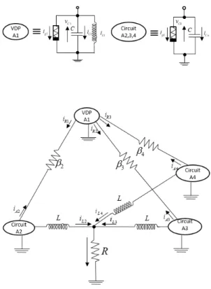
The van der Pol oscillator is a simple circuit as shown in Fig. 1. It consists of an inductor, a capacitor and a nonlinear resistor.
Figure 1: van der Pol oscillator.
In this study, we propose a new type of coupled van der Pol oscillators: Star structure connected to another oscillator. By carring out computer simulations and theoretical analysis, the relationship of the model between synchronization phenom- ena and coupling strength is investigated.
2. Circuit Model
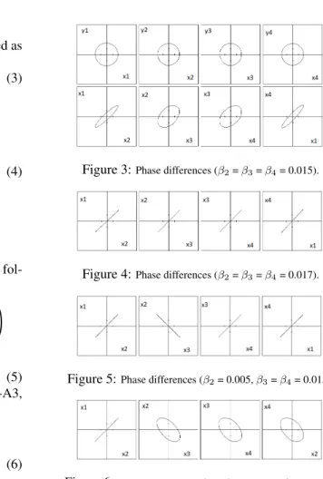
The proposed circuit is shown in Fig. 2. We use three van der Pol oscillators coupled as star structure that connected to another oscillator via resistors r. We investigate synchroniza- tion phenomena by changing coupling strength of the resis- tors.
Figure 2: Circuit model.
- 76 -
IEEE Workshop on Nonlinear Circuit Networks December 7-8, 2018
With v
C1v
C2, v
C3, and v
C4denote capacitor’s voltage and i
L1i
L2, i
L3, and i
L4denote inductor’s electric current.
The circuit equations of VDP-A1 are given as folows:
C dv
C1dt = − i
g1− i
L1− i
R1− i
R2− i
R3, L di
L1dt = v
1.
(1) The circuit equations of Circuit-A2, Circuit-A3, Circuit- A4 are given as follows:
C dv
Ckdt = − i
gk− i
Lk+ i
Rk, L di
Lkdt = v
k− R
∑
4 m=2i
Lm.
(2)
where:
i
Rk= v
1− v
kr , (k = 2, 3, 4).
The characteristics of the nonlinear resistors are defined as follows:
i
gk= − g
1v
k+ g
3v
3k. (3) By changing the variables and parameters:
t = √
LCτ, v
k=
√ g
13g
3x
k, i
Lk=
√ g
1C
3g
3L y
k, α = g
1√ L C , β = 1
r
√ L C , γ = R
√ C L ,
(4)
(k = 1, 2, 3, 4).
the normalized circuit equations of VDP-A1 are given as fol- lows:
dx
1dτ = α (
x
1− 1 3 x
31)
− y
1− β (
3x
1−
∑
4 m=2x
m)
dy
1dτ = x
1.
(5) the normalized circuit equations of Circuit-A2, Circuit-A3, Circuit-A4 are given as follows:
dx
kdτ = α (
x
k− 1 3 x
3k)
− y
k+ β(x
1− x
k) dy
kdτ = x
k− γ
∑
4 m=2y
m,
(6)
(k = 2, 3, 4).
where parameters α, β, and the γ denote nonlinearity, the resistors r, and the resistor R, respectively.
3. Simulation Results
For the computer simulations, we calculates Eqs. (2)-(3) by using Runge-Kutta method with the step size h = 0.05.
When the parameters are fixed as α = 0.1,γ = 0.006, we control synchronization phenomena of this circuit model by changing the coupling strengths β
2, β
3, β
4.
First, in the case of parameters β
2, β
3, β
4are set to 0.015, Fig. 3 shows the attractor of each oscillator. Next, we sightly increase the parameters β
2, β
3, β
4to the same value as 0.017, all fours oscillators become in-phase as Fig. 4. When we only change β
2to 0.005, the oscillator of Circuit A2 becomes anti-phase with other oscillators, when we change β
2, β
3to 0.0005, oscillator of VDP-A1 becomes in-phase with oscil- lator of Circuit A2 and the oscillators of Circuit A2, A3, A4 become 3-phase synchronization. These results are shown in Figs. 5-6.
Figure 3:
Phase differences (β2=β3=β4= 0.015).Figure 4:
Phase differences (β2=β3=β4= 0.017).Figure 5:
Phase differences (β2= 0.005,β3=β4= 0.015).Figure 6:
Phase differences (β2=β3= 0.0005,β4= 0.015).Figures 7, 8 and 9 show the computer simulation results in each case when parameters β
2, β
3, β
4are changed in ranges of values. From these result, we can control synchronization phenomena of this system by changing coupling strengths.
- 77 -
Figure 7:
Phase differences in the case of changingβ2.Figure 8:
Phase differences in the case of changingβ2,β3.Figure 9:
Phase differences in the case of changingβ2,β3,β4.Therefore, we can control synchronization phenomena by changing the coupling strengths.
4. Theoretical Analysis
In this section, we apply theoretical analysis to comfirm above computer simulation results by using averaging method for Eqs. (5) and (6). We assume that x
1,k, y
1,kcan be consid- erd as below:
x
1,k(τ) = ρ
1,k(τ) cos(τ + θ
1,k(τ))
y
1,k(τ) = ρ
1,k(τ) sin(τ + θ
1,k(τ)). (7) Assign Eqs. (5)-(6) to Eq. (7), we obtain:
VDP-A1:
ρ
.1= α(x
1−
13x
31) cos ϕ
1− y
1cos ϕ
1− β (3x
1− ∑
4n=2
x
n) cos ϕ
1+ x
1sin ϕ
1≡ X
1 .θ
1= x
1cos ϕ
1ρ
1− α(x
1−
13x
31) sin ϕ
1ρ
1+ y
1sin ϕ
1ρ
1+
β (3x
1− ∑
4n=2
x
n) sin ϕ
1ρ
1− 1 ≡ Y
1.
(8)
Circuit-A2, Circuit-A3, Circuit-A4:
ρ
.k= α(x
k−
13x
3k) cos ϕ
k− y
kcos ϕ
k+β(x
1− x
k) cos ϕ
k+ x
kcos ϕ
k− γ
∑
4 n=2y
nsin ϕ
k≡ X
k.
θ
k= x
kcos ϕ
kρ
k− α(x
k−
13x
3k) sin ϕ
kρ
k+ y
ksin ϕ
kρ
k− γ
∑
4 n=2y
ncos ϕ
kρ
k− 1 ≡ Y
k,
(9)
where
ϕ
k= τ + θ
k(k = 2, 3, 4) .
By averaging Eqs. (8)-(9) over on period, as averaging method’s theory, ρ
1,kand θ
1,kcan be considered as constant and the values of ρ
.1,
.
θ
1can be calculated as:
VDP-A1:
ρ
.1= lim
T→∞
∫
T 0X
1dτ
.
θ
1= lim
T→∞
∫
T 0Y
1dτ .
(10)
Circuit-A2, Circuit-A3, Circuit-A4:
ρ
.k= lim
T→∞
∫
T 0X
kdτ
.
θ
k= lim
T→∞
∫
T 0Y
kdτ .
(11)
By solving the above equations, Eqs. (10) and (11) are ob- tained:
VDP-A1:
ρ
.1= 1
2 αρ
1− 1
8 αρ
13+ β 3 2 ρ
1+
∑
4 n=21
2 βρ
ncos(θ
n− θ
1)
.
θ
1= 1 2
∑
4 n=2ρ
nρ
1sin(θ
n− θ
1).
(12)
- 78 -
Circuit-A2, Circuit-A3, Circuit-A4:
ρ
.k= 1
2 αρ
k− 1
8 αρ
k3+ 1
2 βρ
1cos(θ
1− θ
k) + 1
2 βρ
k−
∑
4 n=21
2 γρ
ncos(θ
n− θ
k)
.
θ
k= 1 2
∑
4 n=2ρ
nρ
ksin(θ
k− θ
n).
(13)
In the steady state, ρ
1,k.= 0 and
.
![Figure 11: Circuit experiment for r 2 = r 3 = 82[kΩ], r 4 = 2[kΩ].](https://thumb-ap.123doks.com/thumbv2/123deta/7315855.2423523/4.892.563.704.438.537/figure-circuit-experiment-for-kω-kω.webp)
