approach for embedded systems
著者 大谷 寿賀子
著者別表示 Otani Sugako journal or
publication title
博士論文本文Full 学位授与番号 13301甲第4319号
学位名 博士(工学)
学位授与年月日 2015‑09‑28
URL http://hdl.handle.net/2297/43866
Creative Commons : 表示 ‑ 非営利 ‑ 改変禁止 http://creativecommons.org/licenses/by‑nc‑nd/3.0/deed.ja
博 士 論 文
Low power processor architecture and multicore approach for embedded systems
組込み用途向け低消費電力プロセッサ・ア ーキテクチャとマルチコア研究金沢大学自然科学研究科 電子情報科学専攻
学籍番号(
1323112001
) 氏 名 大谷 寿賀子主任指導教員名 新居 浩二 提出年月
‘15/10/28
Contents
Contents ... 1
List of Figures ... 6
List of Tables ... 9
Acknowledgements ... 11
Chapter 1 ... 13
Introduction ... 13
Chapter 2 ... 17
Applications and System Trends ... 17
2.1 Four Key Technologies that support IoT ... 17
2.2 Research Goals ... 19
Chapter 3 ... 21
Low-Power MCU Processor Architecture ... 21
3.1 Microcontroller Basic Strcture ... 21
3.2 Basic Design Approach for Energy Saving ... 22
3.3 Introduction to Low-Power Architecture ... 24
3.4 Core features to boost performance ... 27
RX Architecture Overview... 27
RXv2 Pipeline Design ... 27
Pipeline integrated FPU ... 28
DSP with wide accumulators ... 29
Embedded memory system architecture ... 31
Improving instruction fetch effectiveness ... 31
AFU: Advanced Fetch Unit... 32
Processor performance and power consumption ... 34
Core features to make code compact ... 37
3.6 RX instruction set architecture ... 37
Overview of Instruction set ... 37
Optimized op codes leads to superior code density ... 38
Data Transfer instruction ... 40
1byte conditional branch instruction ... 44
Compare instruction ... 45
3-operand instruction ... 47
Registers ... 48
Code size evaluation ... 51
3.7 Related Works... 52
3.8 Summary ... 54
3.9 List of RX instruction Set ... 56
Arithmetic and logical instructions ... 56
Floating-point operation instructions ... 57
Data Transfer instructions ... 58
Branch Instructions ... 59
Bit manipulation instructions ... 60
String manipulation instructions ... 60
System control instructions ... 61
DSP function instructions... 62
Chapter 4 ... 63
PEACH: A Multicore Communication SoC with PCI Express I/F ... 63
4.1 Introduction ... 63
4.2 PEACH Architecture ... 65
PEACH overview ... 65
Chip Architecture ... 67
PCI Express interface with up-configuration function ... 69
PCI Express up-configuration function ... 71
Intelligent Interrupt Controller ... 73
4.3 Network Managing ... 74
Data Flow Control ... 74
PEARL network route construction ... 78
Network system power management ... 78
4.4 Evaluation System ... 78
PEARL system board ... 78
Switching time of PCI Express up-configuration function ... 81
4.5 Related Works... 81
4.6 Summary ... 82
Chapter 5 ... 83
5.1 Introduction ... 83
5.2 Secure Media System ... 84
Concept of the secure media system ... 84
SoC Overview ... 87
Physical Integration of the SoC and the SiP ... 89
Protection by Software ... 90
5.3 Multicore Hypervisor ... 91
Micro Clustering Model ... 91
Functions of the multicore hypervisor ... 92
Startup sequence ... 93
Inter-OS Communication ... 94
Interrupt handling ... 94
Hypervisor Operating System ... 95
5.4 System Software ... 96
Software Architecture ... 96
Secure media block software... 97
Task mapping ... 98
5.5 System Evaluation ... 100
Evaluation system ... 100
Evaluation results ... 101
5.6 Related Works... 103
5.7 Summary ... 104
Chapter 6 ... 105
Conclusions ... 105
6.1 Future work ... 105
References ... 107
Publications ... 112
List of Figures
Figure 1.1 Thesis outline ... 14
Figure 2.1 Four key technologies that support IoT ... 18
Figure 3.1 MCU (Microcontroller) Basic Structure ... 21
Figure 3.2 Intermittent operations for reduction in power consumption ... 22
Figure 3.3 Power break down of a microcontroller ... 23
Figure 3.4 RXv2 CPU block diagram. ... 25
Figure 3.5 Overview of RXv2 CPU core ... 25
Figure 3.6 RX core road map ... 26
Figure 3.7 Benchmark Comparison ... 26
Figure 3.8 RXv2 pipeline structure ... 28
Figure 3.9 The Coprocessor-type FPU and the pipeline integrated-type FPU (proposed) ... 28
Figure 3.10 RX DSP functionality ... 30
Figure 3.11 MCU: High-Capacity Internal Flash ... 32
Figure 3.12 Fetch Unit for Microcontroller with Advanced Fetch Unit ... 33
Figure 3.13 Embedded Flash processing performance ... 33
Figure 3.14 Benchmark Results of DSP Algorithm programs such as FFT, IIR filter and Matrix under zero-wait flash memory access. ... 35
Figure 3.15 Performance Comparison of RXv2 with RXv1 and a RISC processor ... 36
Figure 3.16 RX instruction set architecture ... 38
Figure 3.17 Analysis of Instruction Frequency ... 39
Figure 3.18 Byte assignment of RX Instruction format ... 39
Figure 3.19 Analysis of general-purpose register configuration ... 49
Figure 3.20 Register Set of the CPU ... 50
Figure 3.21 Code size analysis of the RX and a RISC-based MCU: Static Code Size (a) and Dynamic Code (b). ... 51
Figure 3.22 The test chip of the microcontroller with the RXv2 processor ... 54
Figure 4.1 The communication link, PEARL. ... 64
Figure 4.2 Neighbor communication on PEARL. ... 66
Figure 4.3 PEACH block diagram. ... 67
Figure 4.4 PEACH micrograph. ... 68
Figure 4.5 PCI Express up-configuration function by software control. (a) Maximum data transfer rate (b) Low power consumption. ... 71
Figure 4.6 Power Consumption of PCI Express PHY (W) at each requested transfer volume. . 72
Figure 4.7 Block Diagram of Intelligent ICU ... 74
Figure 4.8 Efficient packet processing and fault handling in PEACH. ... 75
Figure 4.9 Two data transmission flows: Processor mode using interrupt services ... 76
Figure 4.10 The intelligent ICU’s fast automatic data-transfer function improves transfer latency. 77 Figure 4.11 Prototype of PEARL network system. ... 80
Figure 5.1 Implemented secure media system board ... 84
Figure 5.2 Concept of the secure media system. ... 86
Figure 5.3 Block diagram of the SoC ... 86
Figure 5.4 Micrograph of SoC and SiP. ... 89
Figure 5.5 Protection by software ... 90
Figure 5.6 Multicore hypervisor and micro clustering model. ... 92
Figure 5.8. Interrupt operation. ... 95
Figure 5.9. Software layer configuration ... 97
Figure 5.10. Task structure in the secure media block ... 98
Figure 5.11. Task mapping in the secure media block ... 99
Figure 5.12. Data-flow of decoding MP4 container file. ... 99
Figure 5.13. Implemented evaluation system ... 100
Figure 5.14. Block diagram of the evaluation system ... 101
Figure 5.15. Comparison of workload of CPU#1. ... 102
Figure 5.16. Workload balance. ... 103
List of Tables
Table 3.1 Design Highlights of a Low Power CPU ... 23
Table 4.1 PEACH Chip Features ... 70
Table 4.2 Comparison of Power Efficiency ... 70
Table 4.3 Power Consumption of PCI Express PHY (Normalized) ... 72
Table 4.4 PCI Express up-configuration function-switching time. ... 81
Table 5.1 Functional features of the SoC ... 88
Table 5.2 Physical features of SoC and sip ... 88
Table 5.3 Combinations of Supported OSs ... 96
Table 5.4 Workload of CPU#1 in Secure Media Block ... 102
Acknowledgements
Research in microprocessor architecture requires a team effort. During my research, I was fortunate to work with great people who influenced the direction and the quality of my work.
First, I would like to thank Koji Nii, my thesis advisor, for his overall guidance and support.
I am especially grateful to Yoshio Matsuda, my thesis advisor, and Toru Shimizu, my former thesis advisor now at Keio University, for providing me with the opportunity to study as a doctoral student and for their encouragement.
I am especially grateful to Hiroyuki Kondo, a chief processor architect at Renesas Electronics Corporation, for mentoring me. He helped me develop a passion for research and encouraged me to pursue developing microprocessor architecture. Our numerous discussions had a strong influence on my research.
I also want to thank following people: Kunle Olukotun at Stanford University. His guidance
motivated me to cultivate multicore processor architecture. Kazutami Arimoto, at Okayama Prefecture University, Taisuke Boku at Tsukuba University, Toshihiro Hanawa at Tsukuba University and Christoforos Kozyrakis at Stanford University. They gave me valuable advice for my researches and papers. Kazuya Ishida, Isao Kotera and Naoshi Ishikawa, my colleagues at Renesas Electronics
Corporation with whom I have been working together for more than ten years. Without their persistence and selflessness, our progress would not have been possible.
No acknowledgments page would be complete without thanking Ellen Higuchi for wrestling with my technical papers and giving plausible English expressions.
Finally, I want to thank my parents, Shigeki and Sueko Otani, my brother Hiroyuki Otani, for their love and unwavering support.
The PEACH project was supported by a JST/CREST program entitled “Computation Platform for
Power-aware and Reliable Embedded Parallel Processing Systems”.
Development Organization (NEDO), via Grant #0628002.
Introduction
“IoT” or “Internet of things” formerly known as “ubiquitous computing” has been absolutely essential to our society and its infrastructures. Devices are linked to networks from anywhere in the world and will be mutually controlled while information is being exchanged. A microcontroller is one of the important elements of IoT. The microcontroller designers are strongly urged to achieve both high performance computation and low power consumption, which is a hybrid technology with powerfulness of computing and friendliness to the environment. Furthermore, while network services are gaining popularity, dependability and security of network are more important. A key solution to meet these demands is a compact and low power processor core and multicore technology.
This thesis focuses on the development of efficient microcontroller architecture for IoT. The basis for the argument is the key of a low power processor architecture is how effective handle on chip
memories. Furthermore, collaboration of software and hardware on multicore architecture can provide dependable and secure networks.
Thesis Contributions
The main contributions of this dissertation are:
•
An RX processor core which is suitable for IoT. The RX processor Instruction set architecture (ISA) and its microarchitecture can achieve lower power consumption and boost performance.
•
An eight-core communication SoC with PCI Express interface. The multicore SoC can realize a high-performance, power-aware, highly dependable network.
•
A secure multimedia system that uses heterogeneous multicore SoC and software
virtualization.
Figure 1.1 Thesis outline
The outline of the remainder of this thesis is as follows (Figure 1.1).
Chapter 2 provides the background and motivation for this work. It discusses the characteristics and requirements of IoT by presenting four key IoT technologies.
Chapter 3 introduces RX processor core with a low-power processor architecture. The RX processor instruction set architecture (ISA) and its microarchitecture can achieve lower power consumption and boost performance. RXv2 reaches 4.5 Coremark per MHz and the RXv2 processor delivers
approximately more than 2.2 – 5.7x the power efficiency of the previous work. The RXv2 processor delivers 1.9 – 3.7x the cycle performance of previous work in digital signal applications. This chapter is from [S. Otani and H. Kondo, “RX v2: Renesas’s New-Generation MCU Processor,” IEICE
Transactions, Vol. E98-C, No. 7, pp. 544-549, Jul. 2015, (copyright ©2015 IEICE).]
Chapter 4 presents an eight-core communication SoC with PCI Express interface. PEACH with four PCI Express ports realizes high-performance communication of 4 x 20Gbps and power efficiency of 0.04W/Gbps. The power efficiency of InfiniBand 4X (Commodity network devices) is 0.083W/Gbps.
Thus, PEACH provides 51.5% better power efficiency than InfiniBand 4X. We also evaluate the PEARL network system and demonstrate its fault-tolerant ability. This chapter is from [S. Otani, H.
Kondo, I. Nonomura, T. Hanawa, S. Miura and T. Boku, “Peach: A Multicore Communication System
[Chapter2] Background and Motivation
2.2 Four key technologies that supports IoT
3: Network Technology
1: Technology to control sensors, motors and other devices 2: Low Power technology
4: Security technology
2.1 Applications and System Trends
[Chapter 4] A Multicore Communication SoC with PCI Express I/F
[Chapter 5] A Heterogeneous Multicore SoC for Secure Multimedia Applications
[Chapter 3] A Low Power MCU Processor Architecture
[Chapter 6] Conclusions and Future work
• Atomic operation of payment and viewing
• Multicore SoC and SiP for faster communication and decryption
• Hardware / software virtualization for strong security
• Energy saving architecture
• Instruction set
• Processor microarchitecture
• Instruction memory fetch mechanism
• High-performance internode communication by using PCI Express
• Network managing by multicore
for high-dependable and power-aware system
on Chip with PCI Express,” IEEE Micro, vol. 31, no. 6, pp. 39-50, Nov.-Dec. 2011, copyright ©2011 IEEE).]
Chapter 5 demonstrates a secure multimedia system by using a heterogeneous multicore SoC with SiP and software virtualization. The multicore hypervisor virtualizes hardware resources and prohibits operating systems and applications from accessing hardware resources directly. This chapter is from [H.
Kondo, O. Yamamoto, S. Otani, N. Sugai, and T. Shimizu, “Software architecture of a secure multimedia system using a multicore SoC and software virtualization,” in IEEE Int. Conf. Consumer Electronics, Dig. Tech. Papers, pp. 1-2, Jan. 2009, (copyright ©2009 IEEE)]
Finally, Chapter 6 concludes the thesis and suggests directions for future work.
Applications and System Trends
The IoT, or Internet of Things, has become popular. Giving intelligence to devices and connecting them together creates new value.
With the diffusion of IoT, devices operate independently and work autonomously. If IoT is employed, devices can be linked via networks, working autonomously to provide a pleasant environment for people working in the office, in the city, at home and in the factory.
IoT is experiencing rapid evolution. In 2020, the year of the Tokyo Olympics, 50 billion devices will be connected to a network. A trillion sensors will be connected to a network [bryzek14]. An era is about to begin in which everything is linked to huge networks.
There are four key technologies that support IoT, 1) network technology to link one device to another, 2) technology to control sensors, motors and other devices, 3) low power consumption technology to raise energy efficiency and 4) security technology (Figure 2.1).
The shift of centralized control and operating systems will accelerate toward distributed systems, and
network servers are no exception. Highly dependable network technology is vital to connect downsized
servers in various locations.
Figure 2.1 Four key technologies that support IoT
The technology to control sensors and security technology to ensure the solid protection of information are particularly important. For example, recent advances in infrastructure technology include construction monitoring, which has been installed in bridges, tunnels, and roads. The number of installations of network cameras to monitor the environment will be five times larger than in 2006.
These monitors can be controlled over the network. But if the systems are hacked, severe incidents and panic ensue. Security technologies can protect society against these risks. IoT is offering comfort and convenience, but with security concerns.
With an increase in the number of devices on networks, power consumption becomes a major issue.
Sensing modules must always be active to collect information and be long-lived in infrastructures.
Centralized control for energy saving via networks is evolving. One of effective way to reduce energy saving is to adopt inverter technologies. The inverter adoption ratio is not high in developing countries. Even in air conditioners which use the largest amount of power, only 50% utilize inverter technology in the world. A 10% increase in world inverter adoption would reduce the number of thermal power plants by 430. There are two reasons that inverter technology has not spread: to avoid
Sensors Sensors
Wirel Wired ess Sensors
Microcontroller
ConverterA/D Data Analysis
Arithmetic Control
Wirel ess RF Sensing Module with Microcontrollers
1.Technology to control sensors, motors and other devices
4. Low Power technology
2. Network technology 3. Security technology
Cloud Computing
difficulty of system design and to meet lower cost requirement by using sensor-less motors. MCU can solve these problem
In IoT applications, it is vital to consider how to link applications and microcontrollers and how to communicate for people with electronics devices.
Given the applications and systems requirements, we consider four key technologies for an efficient microcontroller architecture for IoT systems:
•
Network technology
•
Security technology
•
Technology to control sensors, motors and other devices
•
Low-power technology
The above features of the architecture and microarchitecture techniques are presented in the
following chapters.
Low-Power MCU Processor Architecture
MCUs (microcontrollers), which control electric devices, consist of CPUs, memories and peripheral interfaces. Figure 3.1 shows the basic structure of MCUs. The CPU reads instructions, decodes and executes arithmetic operations and read/write data. Memories store program code and data. Peripheral interfaces connect the CPU and I/O devices. There are two types of memories. Flash memory is a ROM (Read Only Memory) which mainly stores instructions and retains data even if power is turned off.
SRAM is a RAM (Random Access Memory) which stores data. This working memory loses data if power is turned off. The feature that most distinguishes MCU from MPU (microprocessor units) is integration of the memory system. This feature contributes to low power consumption by eliminating wiring between external memories and a chip.
Figure 3.1 MCU (Microcontroller) Basic Structure
Output Devices
Motors, LEDsetc
Input devices
Sensors, Switches
etc
Microcontroller Processing
Input Output
reads, CPU
decodes and executes instructions
Memories
store instructions
and data
Peripherals
connect devices to CPU
Flash
(ROM) SRAM
(RAM)
The basic strategy of reducing power consumption is to lower the operating current and shorten the operating time. Figure 3.2 shows the difference in power consumption of a low-power microcontroller with another microcontroller. The blue bar represents an energy-saving microcontroller with lower operating current and higher performance. The low-power microcontroller completed the same task in much less time, which also enables it to stay in low-power sleep mode longer. This intermittent operations strategy of low-power microcontrollers enables batteries to last a long time.
Figure 3.2 Intermittent operations for reduction in power consumption
Design highlights of a low-power processor architecture are shown in Table 3.1. Three rows are CPU design highlights; instruction set architecture, processor microarchitecture and memory access
mechanism. The check marks indicate the particular design meets the particular requirement.
Current
Operation Sleep Operation Sleep Time
higher performance Lower operating current
Lower sleep current
CPU RequirementsAll three items are vital to achieve high performance. Instruction set architecture and memory access mechanisms contribute to low operating current.
Table 3.1 Design Highlights of a Low Power CPU
MCUs (microcontroller units) with on-chip memory systems substantially reduce energy
consumption compared to MPUs (microprocessor units) with off-chip memory systems because of the wiring capacity between external memories and the chip. However, the low-power requirement of the embedded applications is more and more strict. The power breakdown of a microcontroller is shown in Figure 3.3. A substantial portion of chip power comes from internal Flash memory. Therefore, reducing Flash memory directly affects the reduction of power consumption of the whole microcontroller.
Considering microcontroller structure, the greater part of the Flash accesses comes from instruction fetches.
Figure 3.3 Power break down of a microcontroller
Requirement High
Performance Low Operating
Current
D esi gn H ig hlig ht s
Instruction Set ✔ ✔
Micro-Architecture (Hardware Structure)
✔ Memory Access
Mechanism
✔ ✔
FLASH 44%
SRAM 8%
CLOCK 13%
Others (CPU, BUS)
35%
Application fields of microcontrollers have spread to building automation, medical devices, motor control, e-metering, and home appliances. The demand for such highly intelligent systems has increased. To meet the demand, the scale and complexity of software has begun to rise. The rapid growth of memory capacity and the advance of microcontroller functions have led to the higher frequency and higher processing performance of embedded processors. Furthermore, many embedded systems still have high cost, power consumption, and space constraints. In order to meet users’ demands for these requirements, new RX processor core (RXv2) architecture has been developed. [otani13].
It is vital for MCUs to handle floating point computation requirements to meet the recent demand for industrial applications. However, the cost of adding an FPU unit to existing MCUs would have been extremely high. The RX includes a compact single precision FPU as a part of the MCU’s basic configuration [linley10], [mips13].
The FPU/DSP functions of the new RXv2 have been enhanced. The RXv2 processor block diagram is shown Figure 3.4. The core has integer, divide, multiply-accumulate and floating point units with sixteen 32bit general purpose registers. Key differences from the previous processor, RXv1, are an improved dual-issue pipeline structure, DSP extensions and a pipelined FPU. The overview of RXv2 specification shows in Figure 3.5.
The RXv2 processor core also incorporates AFU to reduce pipeline branch penalties and Flash memory accesses. The improved power efficiency of the RXv2 architecture with our benchmark evaluation will be discussed in Section 3.5.
Program code is, of course, often the largest consumer of memory in control-intensive applications, affecting both system cost and size. Also, instruction fetches are responsible for a significant portion of power and memory bandwidth. Therefore, both static and dynamic code size are key factors in
embedded systems. RX family instruction set architecture uses variable-length instructions to minimize the static and dynamic code size.
These features have the benefit of boosting performance and making code compact. Figure 3.6 shows
RXv2 CPU core roadmap. RX has two generations, RXv1 and RXv2. Figure 3.7 shows performance
comparison to other embedded processors. RX reaches 4.5 Coremark/MHz on an integer benchmark for
embedded systems.
Figure 3.4 RXv2 CPU block diagram.
Figure 3.5 Overview of RXv2 CPU core
RXv2 CPU
4.5 Coremark/MHz Dual Issue Core
5-stage pipeline
On-chip Debug Memory Protection Unit Integer
Advanced Fetch
Unit
Register Set General
Purpose Registers 16x32-bit
Accumulators 2x72-bit
Control Registers 10x32-bit Divide
Memory Management
Unit
Improved at RXv2
Digital Signal Processing Floating Point MAC
Item Specification
Architecture 32bit CISC
General purpose registers 32bit x 16ch Instructions 109 instructions
Superset of RXv1 (19 new instructions)
Pipeline 5 stage, Dual Issue
DSP function 1-cycle MAC instruction (32bit x 32bit +72bit) Two Accumulators
FPU (Single Precision) IEEE754 compliant data type and exceptions Pipeline processing
Target operating Freq. Up to 240MHz Memory Protection Unit Supported
Performance (Coremark) 4.5 Coremark/MHz
Figure 3.6 RX core road map
Figure 3.7 Benchmark Comparison
RXv1
Performance
Compact
PEACH
(Multiprocessor)
RXv2 Multicore
Higher Frequency Higher Performance
4.5 Coremark/MHz
3.0 Coremark/MHz
RX Architecture Overview
In the past, modern MCUs have added DSP capabilities to create Digital Signal Controllers. Each of these MCUs has limited DSP performance and limited applications. Floating-point math has become essential in various applications such as motor control, factory automation and industrial office automation. However these applications require floating-point math to realize real-time operations.
Adding a DSP/FPU is a logical step to offload compute-intensive work from MCUs. The RX CPU core has been a pioneer in the convergence of MCU and DSP/FPU in the 100MHz midrange market. Both an integrated floating-point unit (FPU) and digital signal processing (DSP) hardware enable the RX to have superior math capabilities.
RXv2 Pipeline Design
The first generation of RX CPU (RXv1) makes use of a single-issue, five-stage pipeline structure.
RXv2 also has the same five-stage pipeline, but a dual-issue core can increase the throughput of IPC
(instructions per cycle) [mips13], [burgess94], [sugure04]. Merely expanding the instruction set
architecture (ISA) is not enough to boost the performance of digital signal applications. High data
supply capability is crucial. Figure 3.8 shows RXv2 pipeline structure. The RXv2 executes FPU/DSP
instructions and memory accesses simultaneously for high data supply. RXv2 supports a dual-issue
integer, float and load/store pipeline. Additionally, the RXv2 can execute various pairs of instructions
simultaneously, so instructions per cycle (IPC) are dramatically improved from the RX.
Figure 3.8 RXv2 pipeline structure
Figure 3.9 The Coprocessor-type FPU and the pipeline integrated-type FPU (proposed)
Pipeline integrated FPU
The most distinguishing feature of RX processors is a pipeline integrated FPU. Most MCUs have a coprocessor-type FPU, which adds inefficient FPU-dedicated registers to load and store results of operations. The pipeline integrated-type FPU used in RX processors can access general purpose
Instruction Fetch
Float
Write Back
Memory Access
IF D E WB
Load/Store MAC ALU, Jump
Float M Divide
ALU, Jump
String F
Decode [Dual Issue]
General Purpose Registers
FPU Coprocessor-type FPU
Load/Store
FPU
General Purpose Registers
Dedicated FPURegisters
Pipeline Integrated FPU
Reduce
Data Transfer Overhead
registers, which reduces data transfer overhead between the FPU registers and general purpose registers (Figure 3.9). This design can also reduce the area of the CPU core by sharing general purpose registers.
The RXv2 FPU has new instructions (SQRT, Float/Integer conversion). Furthermore, the RXv2 FPU instructions employ a three-operand format of FPU instructions to further reduce intermediate variable and waste of register assign.
The new FPU unit adopts pipeline processing to boost throughput and shortens the latency of FPU executions (FADD/FSUB 4cycles -> 2cycles, FMUL 3cycles -> 2cycles). The RXv2 processor performs most operations in one to three cycles and in single-cycle throughput. Adding the three- operand format and speeding up multiply-accumulate operations boost fast Fourier transform (FFT) and Infinite impulse response (IIR) filter performance.
FPU instructions are widely used in various applications and algorithms to achieve a high degree of numeric stability and dynamic range. We expect this upward trend of FPU use in embedded systems and even move into lower-range architectures.
DSP with wide accumulators
One strength of RX DSP architecture is the use of wide accumulators which allows DSP function operations to store their results in a much larger space separated from general purpose registers (Figure 3.10). The MACLO MACHI instructions multiply the 16 bits of a register by the 16 bits of another register, and add the result to the value in the accumulator. At the end of the series of multiply-
accumulate operations, the RACW (Round the accumulator word) instruction rounds and saturates the value of the accumulator into 16bit. The packed 16bit data format of the DSP function operation reduces the number of data memory accesses, which improves digital signal processing performance and decreases power consumption derived from memory accesses.
RXv2 increases the number of accumulators from one to two. The accumulators have been widened from 48 bits to 72 bits. Using two accumulators boosts the performance of fixed-point DSP algorithms.
For example, FIR has parallelism in that each computation result of two series of operations (coefficient
* data) is stored in each accumulator, which reduces the number of data transfers from memory. The
RXv2 DSP function instructions can handle 32bit and 16bit fixed point multiply and multiply-
accumulate operations in a single cycle.
Figure 3.10 RX DSP functionality
In direct contrast to the pipeline-integrated FPU approach, the RX DSP function adopts dedicated accumulators, not general purpose registers to hold calculation results. In DSP algorithms, at the end of the series of data load and multiply accumulate operations, results are referenced. This DSP architecture is assembler-friendly and DSP library programmers can easily tune their programs because of the dedicated accumulators. Register resource shortage is a severe problem for typical MCUs because they have only sixteen general registers. Dedicate accumulators used in RX also solve this problem.
For example, when we execute 32bx32b->64b, four 32-bit registers (two source registers, two destination registers) must be used. To free general registers for other computation, the RXv2 has an EMULA, EMACA, EMSBA (32bx32b->ACC, ACC±32bx32b=ACC) instruction that stores 64-bit results in the accumulators. These instructions uses only two general registers instead of four registers.
As we mentioned before, the dual-issue pipeline exploits parallelisms in DSP operations and memory accesses, which can make full use of DSP computation ability by feeding enough data from memories.
Of course some applications such as VoIP will require a dedicated DSP chip. But many sensor, speech and audio applications can be implemented by MCUs with RXv2.
RACW
Accumulator Accumulator 16bit
Saturate Round Sign extension
MACLO 16bit X + Register
16bit
Register Accumulator Accumulator
X +
MACHI 16bit 16bit 72bit
72bit
72bit 72bit General
Purpose Registers
MAC
MAC Instructions
Free
General Purpose Registers
General Purpose Registers
MAC
72bit ACC0 72bit ACC1
MAC with wide-accumulators
Shift Round
Clip
Embedded memory system architecture
As described in Section 3.2, Flash memory consumes a substantial portion of power in the
microcontroller. Program code is located in flash memory, so the key strategy for low operating current is to reduce instruction memory accesses.
To reduce instruction memory accesses, a cache system is inevitable in today’s embedded microcontrollers. Even though a top-priority issue is energy saving, it is absurd to sacrifice no-wait internal Flash memory performance by using a cache system. Reducing the power consumption of internal memories can be achieved by replacing a portion of large memories with large power consumption with memories with smaller power consumption.
Improving instruction fetch effectiveness
The importance of the memory hierarchy has increased with advances in the performance of
processors. An embedded microcontroller has high-capacity embedded Flash memory, which is equal to the performance in 100% hit cache (Figure 3.11). However, when slower Flash is used, wait-states are required because the CPU operates faster than the native speed of the Flash memory, causing the CPU to stall, which degrades overall performance.
A typical approach is to add an instruction cache between the CPU decoder and the Flash memory.
There are two reasons to add an instruction cache. First, we need to mitigate a processor-memory speed
gap to feed the CPU enough instructions. Second, we also need to reduce flash memory accesses to
lower the power consumption. A large fraction of the total power budget of the microcontroller is the
energy consumption in the path from the FLASH memory to the CPU. Therefore, decreasing the
number of flash memory accesses is crucial in reducing power consumption. The two pillars of RXv2’s
low power consumption are to adopt AFU and variable length ISA. First, variable length ISA delivers
small dynamic code size (described in detail in Core features to make code compact), which can reduce
instruction memory bandwidth. Next, if the requested instruction is contained in AFU, this request can
be handled by simply reading AFU.
Figure 3.11 MCU: High-Capacity Internal Flash
AFU: Advanced Fetch Unit
AFU was added between the CPU decoder and the Flash memory (Figure 3.12). A new branch target cache [bray91] in AFU collaborates with instruction queue (IQ).
Several performance-cost trade-offs were considered in order to determine AFU structure. The RX utilizes our company’s industry-leading 40nm flash technology which enables 120MHz operation with zero-wait states (Figure 3.13). Fetch latency from the Flash memory to CPU decoder directly is one cycle. Therefore, RXv2 can avoid instruction pre-fetch performance degradation. This small processor- memory speed gap allows us to concentrate on mitigating the branch penalty to improve performance.
RXv2 benefits from adopting a branch target cache, which has a comparatively smaller area than that of a typical cache systems.
Decode CPU External
Memory
IQ Select Processor
Cache
Embedded Microcontroller
Decode CPU IQ
Select Embedded Flash
= 100% Hit Cache
No-wait
Figure 3.12 Fetch Unit for Microcontroller with Advanced Fetch Unit
Figure 3.13 Embedded Flash processing performance
D-stage IF-stage
Decoder IQ Select
Typical Approach Embedded
Flash Inst.
Cache
Embedded RXv2 Flash
AFU
Decoder IQ
Select Branch
Target Cache
No-wait
• Industry’s only 120MHz embedded Flash process
D
IF E WB
D
IF E WB
IF D
IF E WB
D
IF E WB
IF D
IF E WB
D
IF E WB
IF
RX with 120MHz Flash No-wait Flash
120MHz
Competing MCU
with 30MHz Flash
AFU consists of an IQ and a small fully-associative branch target cache with LRU replace algorithm.
AFU has the following functions:
- storing branch target code (branch target cache
)- detering unused prefetching (instruction queue reuse in small loops, prefetch stop when JUMP instruction is detected.)
-replacing a cache line under dynamic priority control (8-entry LRU, Adaptive lock etc.) AFU and zero-wait embedded Flash can reduce power consumption and improve performance because AFU reduces memory accesses and zero-wait Flash memory does not deliver cache miss penalty. AFU makes instruction buffering decisions on the fly based on an analysis of program flow.
When a short loop code is detected, AFU can reuse fetched instructions in IQ and the branch target cache. IQ is locked to protect codes in the loop. This short-loop buffering reduces both branch penalties and eliminates flash memory accesses at a lower cost than that of a typical approach such as a loop- cache which stores the whole loop code.
Another efficient utilization of fetched data from memory is “fast short forward branch”. The CPU core sends the distance to the branch target. If IQ finds the target code in IQ, CPU fetches codes from IQ without a pipeline flash and memory accesses. This technique improves if-then-else control flow in cycle performance and power dissipation.
AFU of RXv2 improves its processing performance by 6% in Coremark [halfhill09] with zero-wait Flash memory.
Processor performance and power consumption
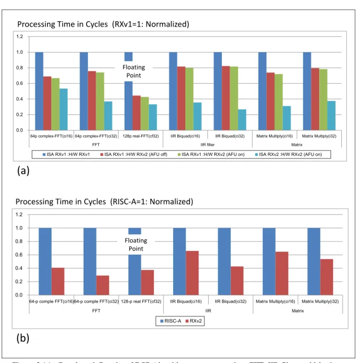
Differences in performance appear when benchmarking DSP programs that include numeric
operation function such as filter programs. Figure 3.14 illustrates that the DSP of RXv2 has contributed
mainly to performance improvements compared to RXv1 when executing FFT, IIR and Matrix under
16bit fixed point, 32bit fixed point and float conditions. The RXv2 processor delivers 1.9 – 3.7 the cycle
performance of the RXv1. As a result, the RXv2 provides 1.5 – 3.4 the cycle performance of a RISC-
based processor. RXv2 achieves performance as high as commonly used DSP and improves far more as a DSP microcontroller.
Figure 3.14 Benchmark Results of DSP Algorithm programs such as FFT, IIR filter and Matrix under zero-wait flash memory access.
Breakdown of the RXv2 performance enhancement from the RXv1 (a), Performance comparison to a RISC-based processor (Cortex-M4) (b).
0.0 0.2 0.4 0.6 0.8 1.0 1.2
64p complex-FFT(ci16) 64p complex-FFT(ci32) 128p real-FFT(cf32) IIR Biquad(ci16) IIR Biquad(ci32) Matrix Multiply(ci16) Matrix Multiply(i32)
FFT IIR filter Matrix
ISA RXv1 :H/W RXv1 ISA RXv1 :H/W RXv2 (AFU off) ISA RXv1 :H/W RXv2 (AFU on) ISA RXv2 :H/W RXv2 (AFU on)
Floating Point
(a)
Processing Time in Cycles (RXv1=1: Normalized)
0.0 0.2 0.4 0.6 0.8 1.0 1.2
64-p comple FFT(ci16)64-p comple FFT(ci32) 128-p real FFT(cf32) IIR Biquad(ci16) IIR Biquad(ci32) Matrix Multiply(ci16) Matrix Multiply(i32)
FFT IIR Matrix
RISC-A RXv2
Floating Point
(b)
Processing Time in Cycles (RISC-A=1: Normalized)
Figure 3.15 Performance Comparison of RXv2 with RXv1 and a RISC processor
We evaluated the performance and power dissipation of the RXv2 device (120MHz) in a simulation with gate-level power analysis using actual loading. RXv2 reaches 4.5 Coremark per MHz. RXv2 achieved a 50% - 150% improvement in various performance categories compared to existing products.
The result is performance that outperforms the competing RISC microcontrollers. Figure 3.15 illustrates the performance advantage of the RXv2 device compared to the RX device. The RXv2 processor
0.0 0.2 0.4 0.6 0.8 1.0 1.2 1.4
RISC RXv1 RXv2
0.0 0.5 1.0 1.5 2.0
RISC RXv1 RXv2
0.0 0.5 1.0 1.5 2.0 2.5
RISC RXv1 RXv2
Operating Current Processing
Performance Power Efficiency
(RXv1=1:Normalized)
[mA] [Coremark] [Coremark/mA]
(a) Coremark
0.0 0.2 0.4 0.6 0.8 1.0 1.2
RXv1 RXv2
0.0 0.2 0.4 0.6 0.8 1.0 1.2 1.4 1.6
RXv1 RXv2
0.0 1.0 2.0 3.0 4.0 5.0 6.0
RXv1 RXv2
Operating Current Processing Performance
(RXv1=1:Normalized)
[mA] [Performance] [Performance/mA]
(b) Small loop program
Power Efficiency
Frequency RISC/SH2A (120MHz), RXv1 (100MHz), RXv2 (120MHz) Process, Voltage Under 40nm process, 1.2 V (internal)
Modules CPU Subsystem (CPU + Internal Bus + SRAM + Flash)
delivers approximately more than 2.2 – 5.7x the power efficiency of the RXv1 in executing Coremark and a small loop program (a power evaluation program). Figure 3.15(a) also illustrates that the RXv2 processor achieves 5.2x the power efficiency of a RISC processor (SH-2A), which shows that the performance of RXv2 is sufficient to fulfill the performance requirement for current and future embedded systems. The decrease of the number of Flash memory accesses by AFU is a dominant determiner of reducing power consumption in benchmarks. AFU reduces the number of Flash memory accesses by 25%.
Core features to make code compact
Small memory size is inevitable in embedded applications because of their severe cost constraints, especially in MCUs with on-chip memories [bunda93]. Furthermore, program compression has a benefit for energy saving by reducing the number of bit fetched from memories. Several RISC
architecture machines offered a mix of 16bit and 32bit instructions to compensate for the disadvantage of the code density. Despite the effort to mitigate this penalty, RISC MCUs still have basically inferior code density because of the lesser work accomplished per instruction [mips13], [sugure04], [xarm10].
Overview of Instruction set
RX has a compact architecture with 109 carefully-selected instructions, which is equal to the number of instructions in a RISC-based architecture (Figure 3.16). The RX instruction set consists of eight types of instructions: arithmetic/logic instructions, floating-point operation instructions, data transfer
instructions, branch instructions, bit manipulation instructions, string manipulation instructions, system control instructions and DSP function instructions [renesas13].
To achieve a high performance, high code density and low power system, the RX instruction set
architecture uses a variable-length instruction format (1byte – 8byte). The RX instructions are variable
in length at the byte level with the exact instruction length dependent on the data size and addressing
mode used, which increases instruction code density and reduces the amount of data fetched from
memory per operation.
Figure 3.16 RX instruction set architecture
Optimized op codes leads to superior code density
CISC architecture inherently has the advantage in terms of the work accomplished per instruction and that always translates to a code-density win [hennessy06]. RX architecture stretches that advantage via a flexible instruction set architecture that can encode some instructions in as little as one byte.
At the other end of the spectrum, instructions can takes as many as eight bytes when the instruction needs to specify a large address range or large data values that are unable to handle 32bit instructions.
We did a further analysis of real application code to discern the most frequently used instructions and further reduce code size (Figure 3.17). We determined the most frequently used instructions are
assigned to shorter instruction codes, from one-byte to four-byte instructions. We also added addressing modes and included a three-operand instruction format to optimize code density.
ABS MAX RORC MOV POP PUSHC SCCnd EMACA MSBLO MVTACGU
ADC MIN ROTL MOVCO PUSH PUSHM STNZ EMSBA MULHI MVTACHI
ADD MUL ROTR MOVLI POPC REVL STZ EMULA MULLH MVTACLO
AND NEG SAT MOVU POPM REVW XCHG MACHI MULLO RACL
CMP NOP SATR Branch Strings MACLH MVFACGU RACW
DIV NOT SBB BRK MVTC Bcnd SCMPU MACLO MVFACHI RDACL
DIVU OR SHAR CLRPSW RTE BRA SMOVB MSBHI MVFACLO RDACW
EMUL RMPA SHLL INT RTFI BSR SMOVF MSBLH MVFACMI FTOI
EMULU ROLC SHLR MVTIPL SETPSW JMP SMOVU FTOU
SUB TST XOR MVFC WAIT JSR SSTR FADD FMUL ITOF
RTS SUNTIL FCMP FSUB ROUND
BCLR BMcnd BNOT BSET BTST RTSD SWHILE FDIV FSQRT UTOF
Floating-point Bit manipulation
System manipulation
DSP Data Transfer
Arithmetic/Logic
Figure 3.17 Analysis of Instruction Frequency
Figure 3.18 Byte assignment of RX Instruction format
Assign short code to frequently-used instruction
Relative condition branch:BEQ,BNE Unconditional relative branch:BRA
1byte length Instruction (Frequently-used “Conditional Branch”)
2byte-length Instructions (Frequently-used “Data Transfer and Comparison instructions”)
3byte-length Instructions (Frequently-used “Arithmetic and logical instructions”) Data Transfer :MOV (register to register, memory to memory, Load, Store) Comparison :CMP (register to register, register to immediate)
Addition :ADD (register + register, register + immediate) Subroutine branch :BSR
Multiplication :MUL (register x register)
Division :DIV (register / register)
Multiply-accumulate :EMAC (register x register) Floating-point addition :FADD (register + register) Floating-point multiplication :FMUL (register x register)
more than 30% of all operations. Conditional branch instructions were the next most frequent, followed by Compare instructions, Subroutine Branch instructions and Add (ADD). Move instructions therefore received the most enhancements in terms of additional addressing modes, and the ability to
automatically increment and decrement values stored in registers. The next most frequent instructions were also shortened. Add instructions were both shortened and enhanced with a three-operand format.
Figure 3.18 illustrates RX instruction code that assigns shorter code to frequently used instructions.
The instruction set is decidedly CISC in nature and is a primary factor in the code density and performance advantage. The following is a detailed look at some instructions to illustrate the benefits of the architecture.
Data Transfer instruction
MOV instruction illustrates RX variable length instruction set advantages. Unlike in the RISC case where instructions are generally fixed in length, the CISC counterpart is variable in length and far more flexible. The MOV instruction is the most frequently used instruction in real application code, therefore its binary code assignment instruction is important for execution performance and code size
compression.
The RX MOV instruction can handle the following six types of data transfer from source to
destination.
RX Family RXv2 Instruction Set Architecture User’s Manual: Software (copyright ©2013 Renesas Electronics Corporation)
The RX MOV instruction supports various operand formats and addressing modes. Therefore, programmers and compilers can reduce code size effectively by using appropriate instruction format for the most commonly used instance of MOV.
1. Wide variety of immediate field of MOV instructions.
Immediate value can be selected directly from 8bits, 16bits, 24bits and 32bits with signed and unsigned types. This feature provides the benefit of eliminating operations that set an immediate value to a register.
2. Short-format MOV instructions.
There are a number of short-format MOV instructions that are used most frequently and those instructions are 2 or 3 bytes in length. Consider a typical example of this instruction:
MOV.L Rs, dsp:5[Rd]
This instruction transfers a 32bit value from a source register (Rs) to a memory location that is
defined by the location stored in a destination register (Rd) added to a 5bit displacement value. The
effective address of the operand is the least significant 32 bits of the sum of the displacement (dsp:5)
value, after zero extension to 32 bits and multiplication by 4, and the value in the specified register.
applying limitation on use of general-purpose registers into half of full 16 registers (R0 – R7), both of the register designations are compacted into 3 bits. Therefore, this MOV instruction is encoded only in two bytes. For modern compilers or hand-coded assembly language, this limitation is minor. In
comparison, consider the same instruction with full access to 16 registers and with the range afforded by a 16bit displacement value. That instruction would double in size to 4 bytes. When clever encoding can reduce a powerful instruction from 4 bytes to 2 bytes, the inherent advantage of a CISC instruction set is greatly enhanced.
1byte conditional branch instruction
The conditional branch instruction plays a big part in code density; therefore, it is always encoded in the minimum possible length.
RX Family RXv2 Instruction Set Architecture User’s Manual: Software (copyright ©2013 Renesas Electronics Corporation)
The conditional branch instructions can comprise 15% of the instructions in a typical program – second in frequency only to the MOV instruction. There are conditional branches based on greater than or less than operators, and based on positive, zero, or negative values to offer flexibility to the
programmer.
The RX instruction set encodes such instructions in as compact a length as a single byte on
Conditional Branch instructions including BEQ (branch if equal), BNE (branch if not equal) and BRA (branch always).
Consider the following instructions:
BEQ label1
This BEQ instruction results in a branch to a memory location if the processor's Z flag is set to a value of "1". The instruction length is determined by the difference between the memory location of the BEQ instruction that is stored in the program counter relative to the branch location defined either by a label.
According to program analysis in various applications, most branch distances are within the general vicinity and branch directions are forward in order to execute if-then-else program codes. Therefore RX instruction architecture encodes the branch forward instructions (BEQ, BNE and BRA) with address distance of 10 byte or less in one byte.
The RX supports more branch operations including both in the forward and reverse directions from a memory address perspective. A two-byte instantiation can control forward or reverse branches in the range of -128 to +127 relative to the program counter. And the three-byte version stretches the range to -32768 to +32767.
The result is better performance on application code that occupies a smaller memory footprint.
Compare instruction
The code analysis revealed that the CMP instruction was the third most frequently used instruction.
The instruction comprised 11% of the sample code. Moreover, the design team found a way to cut the
instruction length in half relative to other CISC MCUs – yielding a 2-byte CMP instruction.
RX Family RXv2 Instruction Set Architecture User’s Manual: Software (copyright ©2013 Renesas Electronics Corporation)
The CMP instruction is variable in length depending on the type of the operands. It is a tremendous advantage of a CISC instruction set to be able to use immediate values and operands stored in memory with instructions such as CMP. RISC requires that both operands be stored in registers.
There are three different ways to use CMP with a 2-byte instruction length. Register to register compares are always 2 bytes. But the RX also supports both compares using immediate values and operands from memory with 2-byte instructions.
Consider the following instruction:
CMP #7, R2.
The instruction compares an immediate value 7 with the data stored in R2. As long as the immediate value is 4 bits or less in size, the instruction requires only 2 bytes. But the implementation provides the flexibility to use immediate values as wide as 32bits. The instruction lengths scales from 2 to 6 bytes to support 4, 8, 16, 24, and 32bit immediate values.
The CMP instruction can also be implemented in 2 bytes for memory-to-register compare operations.
Consider the following instruction:
CMP [R2], R3.
This instruction comparing the operand pointed to by R2 with the one stored in R3 always requires
only 2 bytes. Again, however, the implementation offers flexibility. The instruction can be used with a
displacement value from the memory location stored in the register. The instruction length scales to 5 bytes to support 16bit displacements.
Almost all CISC architectures offer the flexibility illustrated here with CMP, which is a huge advantage of CISC relative to RISC.
3-operand instruction
The instruction implementation in the RX offers a variety of addressing modes and even a three- operand format. ADD is the fifth most regularly occurring instruction, making up 6% of the instructions in a typical program; therefore it was targeted for special treatment.
Consider the instructions:
ADD R1, R2, R3 and
ADD R1, R2.
The benefit of three-operand format is not to overwrite one of the source operands and program code can reuse the value of the source register. Both ADD instructions add the values in R1 and R2. The three-operand format stores the result in R3. The two-operand stores the result in R2 – overwriting one of the source operands. With embedded RISC processors that only support the two-operand format, there are times when an extra move instruction is required before or after the ADD because the program needs to preserve the data in the destination register before the ADD takes place as well as preserving the summed result.
The RX ADD instruction offers additional flexibility in that the first of the three operands can be an immediate value. RISC architectures would always have to load such an immediate value prior to executing the ADD.
The three-operand ADD is encoded in three bytes when each of the operands is a register. With an
8bit immediate value, the instruction still only requires 3 bytes. Larger immediate values can stretch the
instruction length to 4, 5, or 6 bytes.
both operands are registers. But we devised 2-byte instructions both for ADDs involving an immediate value or data from a memory location.
A two-operand ADD instruction, in which the first operand is a 4bit immediate value and the second operand is a register, requires only two bytes. That is half the size of typical immediate-value ADD instructions. Larger immediate values stretch the instruction length to 3, 4, 5, or 6 bytes.
A two-operand ADD instruction in which the first operand is data in a memory location that is pointed to by a register also requires only two bytes. More complex versions can use a register storing a memory location, and an offset from that location. Such relative-addressing modes can result in 3-, 4-, or 5-byte instructions. For systems, the result is smaller code, less memory and therefore lower cost, and better performance.
RX Family RXv2 Instruction Set Architecture User’s Manual: Software (copyright ©2013 Renesas Electronics Corporation)
Registers
We have investigated how general-purpose register configurations and operational codes for
instructions are related. The number of registers in an instruction set architecture has a direct impact on
code size because the register number bit field requires more bits in the operation codes to encode
support for more registers. But more registers are almost always better from a performance perspective.
A greater number of registers eases register allocation, which means that the target program spends far less time shuffling data between memory and registers. Even CISC architectures that can directly operate on operands stored in memory still feature faster execution when operating on registers.
To perform an in-depth analysis on the optimal size of a register file, we ran benchmark tests using real code that was central to target markets such as office automation and consumer, industrial, and automotive fields. Figure 3.19 shows the analysis of the register file. The vertical axis on the left represents the relative amount of hardware volume needed to support the register file. Red curves on the right indicate the code size attributable to the number of registers. The green curve indicates the
register-specified bit number in operation code.
Figure 3.19 Analysis of general-purpose register configuration
Figure 3.20 Register Set of the CPU
RX Family RXv2 Instruction Set Architecture User’s Manual: Software (copyright ©2013 Renesas Electronics Corporation)
Eight registers is too small to execute code in real applications in which save/restore operations occur quite frequently, which causes performance degradation and code size increase. The variable length instruction set allows only four bits of register-addressing fields. For register-to-register instructions, at least two register-specified fields are required. Five bits of operation code are specified for 32 registers.
In order to balance performance, hardware cost, and code density, the benchmarks led to the decision
to include sixteen general-purpose registers in the RX architecture. As a result, the RX CPU has sixteen
general-purpose registers, ten control registers, and two accumulators used for DSP instructions (Figure
3.20).
Figure 3.21 Code size analysis of the RX and a RISC-based MCU: Static Code Size (a) and Dynamic Code (b).
Code size evaluation
Figure 3.21 illustrates a code size analysis of the RX and a RISC-based MCU with three different types of applications, a real-time-control application, a motor-control application and system-control application. The implementation delivers up to 46% reduction in static code size, and up to 30%
reduction in dynamic code size relative to RISC architectures. Small static code size makes a significant contribution in decreasing ROM size, and by extension, costs. Small dynamic code size delivers low power consumption as described in the section “Improving instruction fetch effectiveness”.
0.0 1.0
Motor Control System control Real-time control
Static Code Size (relative)
= RX
= RISC-based MCU
46% less
22% less
31% less
0.0 1.0
Motor Control System control Real-time control
Dynamic Code Size (relative)
= RX
= RISC-based MCU
30% less
15% less
15% less