performance benchmarking together with prospects for high productivity and high performance computing enabled by photonics. The exponential and sustained increases in computing and data center needs are driving the demands for exascale computing in the future. Power-efficient and paral- lel computing with balanced system design is essential for reaching that goal as should support∼billion total concurrencies and∼billion core in- terconnections with∼exabyte/second bisection bandwidth. Photonic inter- connects offer a disruptive technology solution that fundamentally changes the computing architectural design considerations. Optics provide ultra- high throughput, massive parallelism, minimal access latencies, and low power dissipation that remains independent of capacity and distance. In addition to the energy efficiency and many of the fundamental physical problems, optics will bring high productivity computing where program- mers can ignore locality between billions of processors and memory where data resides. Repeaterless interconnection links across the entire comput- ing system and all-to-all massively parallel interconnection switch will sig- nificantly transform not only the hardware aspects of computing but the way people program and harness the computing capability. This impacts programmability and productivity of computing. Benchmarking and opti- mization of the configuration of the computing system is very important.
Practical and scalable deployment of photonic interconnected computing systems are likely to be aided by emergence of athermal silicon photonics and hybrid integration technologies.
key words: computing, data centers, optical interconnects, silicon photon- ics
1. Introduction
Ubiquitous computing and cloud computing have become an essential part of our daily lives, and we rely increas- ingly on these computers for everything from healthcare and climate predictions to entertainment and shopping. In the healthcare sector alone, we are seeing rapid transi- tions in data processing from two-dimensional images to three-dimensional or hyper-spectral real-time 3D images.
However, today’s data centers and computing systems have reached scalability power limitations to scale further. Typ- ical data centers are consuming megawatts of power, and the desire to realize exascale computing is seriously chal- lenged by the power limitations projected to approach 0.5 GW power consumption for Exascale computing.
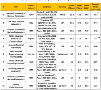
Figure 1 shows the rapid exponential growth of su- percomputer performance based on Top500.org where LIN- PACK benchmarking was used.
Table 1 summarizes the top 10 on the TOP500 list, and Manuscript received January 29, 2014.
Manuscript revised March 17, 2014.
†The author is with the University of California, Davis, Cali- fornia 95616, U.S.A.
a) E-mail: sbyoo@ucdavis.edu DOI: 10.1587/transcom.E97.B.1272
Fig. 1 Rapid growth of supercomputers performance, based on data from top500.org site. The logarithmic y-axis shows performance in GFLOPS.
The red line denotes the fastest supercomputer in the world at the time.
The yellow line denotes supercomputer no. 500 on TOP500 list. The dark blue line denotes the total combined performance of supercomputers on TOP500 list [1].
Table 1 List of Top 10 supercomputers [1].
our current aim at exascale computing by year 2020 is un- realistic unless the energy consumption for operation (En- ergy/Rmax) go at least an order of magnitude below the cur- Copyright c2014 The Institute of Electronics, Information and Communication Engineers
Fig. 2 Energy per flop-historical and projected [6].
Fig. 3 Trend of a number of transistors per integrated circuit, clock speed (MHz), power (W), and performance per clock (ILP).
rent level at∼0.5 nJ/FLOP so that sustained exascale com- puting can be realized at below 10 MW average power con- sumption. Koomey [2], [3] noted in 2010 that the energy efficiency of computing doubles nearly every 1.5 years, but as Fig. 2 illustrates, the Koomey’s law is starting to break down as energy efficiency starts to flatten. At the device level, the Dennard’s law in 1974 [4] describing MOSFET scaling rules for obtaining simultaneous improvements in transistor density, switching speed and power dissipation [4] to follow the Moore’s Law [5], thus doubling every 20 months, has already become obsolete in 2004. (It is of- ten incorrectly quoted as a doubling of transistors every 18 months, as David House, an Intel Executive, gave that pe- riod to chip performance increase. The actual period was about 20 months for doubling the number of transistors).
Figure 3 illustrates the continuation of the Moore’s law while the Dannard’s law has stopped to keep pace with the Moore’s law beyond 2004. As the device dimensions such as gate oxide thickness reduce to several atomic layers, tun- neling and leakage current become significant. The Inter-
Fig. 4 Growth in socket and core count [6].
Fig. 5 Total concurrency trend [6].
national Technology Roadmap for Semiconductors (ITRS) [7] refers to this as a ‘red brick wall’ as there is no known technology solution beyond 2016 when CMOS scaling is expected to stop (note that CMOS power density scaling al- ready stopped in 2004).
Hence, while the number of transistors continue to in- crease, new solutions for improving energy efficiency is no longer about increasing the clock speed in a large single processor, but rather by introducing many small processors running at moderate clock speeds and interconnecting them in a way to support massive concurrencies in parallel at an optimized system performance design configuration. The Amdahl’s law [8] suggests that a parallel computing sys- tem with balanced processing, memory, and communica- tions performs best across most applications. This indicates that for an optimized exascale computing system, we expect to need 1 exabyte/second, or 8 million terabit/second bisec- tion bandwidth. Furthermore, as Fig. 4 and Fig. 5 illustrated, the number of cores and the total concurrency are increasing exponentially, now approaching or exceeding 1 million in a large computing and data systems. Unfortunately, currently most of the computing systems are 10x∼100x misbalanced and deprived of sufficient interconnection bandwidths and parallelism.
It is evident that electronics alone will be unable to meet the requirements of future computing supporting the
rate transparency, and power reduction, without concerns for [10] impedance, crosstalk, voltage isolation, pin induc- tance, signal distortion, and repeater-induced latency. Ex- citing opportunities exist in wavelength routing to reconfig- ure the high-capacity connectivity of multiple wavelengths to reduce contentions and increase system-wide throughput [11], [12]. Recent advances in silicon nanophotonic tech- nologies compatible with nanoelectronics offer new possi- bilities in realizing future computing systems with a very new architecture.
2. Optical Interconnects Everywhere
The opportunity for optical interconnects [13]–[16] in board-to-board and rack-to-rack communications is already well documented. Table 2 illustrates interconnection hier- archy in the computing system for typical dimensions and targeted energy and cost budget to stay competitive against electronic counterparts. The target energy was calculated for local link at each region to pursue exascale computing at below 20 MW power in the near future. ITRS Longterm Roadmap [17], [18] also indicates similar trend.
In addition to the power requirement, what remains ex- tremely challenging is the cost target of the new photonic technologies for practical implementation of exascale com- puting and for market acceptance towards ubiquitous com- puting.
Many literatures [15], [16] already discussed the bene- fits of optical interconnects in detail. Figure 6 illustrates the advantage of the optical link by reducing the cost, power, and complexity compared to the electronic link. Figure 7 shows a generic optical transceiver which requires addi- tional optical components but reduces the requirement for clock and data recovery circuits. Since electrical communi- cation links suffer from RF skin-effects, RF losses, electro- magnetic interference, and limited bandwidths, high-speed parallel data communication need to employ many elec- tronic regenerators including equalization, reshaping, ream- plification, and reclocking. On the other hand, optical datalink has can achieve multi Tb/s communications on par- allel wavelengths with negligible loss, crosstalk, and distor- tion on a fiber such that repeaters become unnecessary for typical data centers or computing centers, and the equalizers can be simpler. Further, optical clock distribution can po- tentially eliminate needs for many clocking circuits in each node.
Fig. 6 Electronic vs. optical data link.
Fig. 7 Optical transmitter and receiver.
In addition to point-to-point data link and data trans- mission, switching and routing of data with optical paral- lelism and reconfigurability greatly facilitates the goals of high-productive exascale computing. The next sections will discuss these aspects in more detail.
3. Optical Switches and Routing in Computing Sys- tems and LIONS
As Fig. 8 indicates, typical computing and data centers uti- lize interconnection of various size electronic switches in many cascaded stages. Due to limitations in radix and bandwidth of the electronic switches, the inefficiency of the cascaded switch stages compounds, especially in terms of latency, throughput, and power consumption. This is one of the key reasons behind challenges of parallel pro-
Fig. 8 Typical data center interconnection topology involving various sizes of electronic switches [19].
Fig. 9 Flattened data center interconnection topology involvingN×N AWGR based LION switch.
Fig. 10 N×N arrayed waveguide grating router’s (a) wavelength routing property (N=5 example), and (b) wavelength assignment table (figures courtesy of NEL).
gramming because the locality constraints for data become very important. On the other hand, optical parallelism and wavelength routing capability of arrayed wavelength grating routers (AWGRs) can collapse the entire network to a single hop and flattened interconnection topology while supporting all-to-all interconnection as shown in Fig. 9.
Arrayed waveguide grating router (AWGR) [20], [21]
is a passive wavelength routing component that enables all- optical switching. The main difference between the elec- tronic crossbar switch and the AWGR switch is that (a) the N ×N AWGR switch provides simultaneously fully con- nected all-to-all interconnection thus providingN2simulta- neous connection links, (b) there is no switching component within the core of the AWGR switch fabric (AWGR is a pas- sive element), (c) the switching component scales linearly as the number of connection links supported by the switch, and (d) the AWGR supports parallel wavelength interconnection covering huge (>20 THz) optical bandwidths. Figure 10 illustrates the (a) wavelength routing property (N=5 exam- ple) and (b) wavelength assignment table for switching of an AWGR. As Fig. 10 demonstrates, the well-known wave- length routing property of theN×NAWGR supports simul- taneous and non-blocking interconnections of each ofNin-
Fig. 11 The system diagram of the proposed rack to rack LIONS optical switch, LD: Label Detector; OLG: Optical Label Generator; PE: Packet En- capsulation; LE: Label Extractor; FDL: Fiber Delay Line; TX: Transmitter;
RX: Receiver; PFC: packet Format Converter; O/E: Optical-to-Electrical converter; E/O: Electrical-to-Optical Converter [22].
put ports with all ofNoutput ports by usingNwavelengths.
For theN=5 example, there areN2=25 simultaneous in- terconnections. Each input port can utilize a wavelength (instead of electronic headers) to address the output port.
For this reason, any input port can use a tunable transmitter to address each output port by tuning the transmitter to the corresponding wavelength without contention if each out- put port is equipped with a wavelength demultiplexers and Nreceivers. Alternatively, theN×NAWGR can be used in all-to-all interconnection without contention by employing Ntransmitters andNreceivers at each port [22].
Figure 11 shows an AWGR based hybrid intercon- necting architecture, referred to as lightwave interconnect optical network switch (LION switch, or LIONS), which also includes optical channel adapters (OCA), tunable wave- length converters (TWC), loopback buffers and the control plane for the switching fabric. LIONS uses label switching with the optical label transmitted on a different wavelength.
We compared the performance of rack to rack LIONS with other state-of-art rack to rack switches including the electrical switching network architecture employing flat- tened butterfly topology, the IBM-Corning’s Optical Packet Switch for Supercomputers (OSMOSIS) and the Data Vor- tex optical switch [23]–[26]. Figures 12(a) and (b) show the effective bandwidth and the end-to-end latency of LI- ONS comparing with a flattened butterfly network under a 32- and 128-node for a message size of 128 bytes. The av- erage end-to-end latency of the flattened butterfly network increases much faster than that of the LIONS system under moderate network load. The flattened butterfly network sat- urates more easily with increasing network size, while the latency of LIONS is almost independent of the size of the network. The effective bandwidth comparison shows that LIONS can support heavy network load of up to 90% and beyond. We simulated the case where the LIONS has a radix of 64 and the message size is 256 bytes (the packet size is 324 bytes) so that the setting is comparable with that of OS- MOSIS demonstrator. At the load of 90%, the latency of LI-
Fig. 12 LION switch comparison with other switches. (a) the effective bandwidth LIONS comparing with a flattened butterfly network under a 32- and 128-node for a message size of 128 bytes, (b) the end-to-end latency of LIONS comparing with a flattened butterfly network under a 32- and 128- node for a message size of 128 bytes, (c) the effective bandwidth compari- son for LIONS vs. OSMOSIS, and (d) the effective bandwidth comparison for LIONS vs. Data Vortex [22].
Fig. 13 Working principle of all-optical token where saturable reflector (reflective-SOA) reflects the first packet with high gain while others with lower saturated gain [28], [29]. (TD: token detector).
ONS is still less than 190 ns. In comparison, the minimum achievable latency of OSMOSIS is above 700 nanoseconds by only considering data path delay as well as STX arbitra- tion [27]. Figure 12(c) shows the effective bandwidth com- parison. LIONS achieves a little higher effective bandwidth than OSMOSIS, because the InfiniBand label is smaller than the total overhead of the OSMOSIS. Figure 12(d) shows the effective bandwidth comparison. Notice that Data Vortex saturates before the uniform network load reaches 0.5 [27].
Clearly LIONS outperforms both OSMOSIS and Data Vor- tex in terms of effective bandwidth. The results also indicate label rate actually affects latency performance of LIONS, higher label rate can reduce the end-to-end latency.
The control plane in Fig. 11 can be distributed by all-optical token and accelerated by all-optical negative acknowledgment mechanisms, combined into all-optical TONAK described in Refs. [28], [29]. Figure 13 illustrates the working principle of all-optical token where saturable reflector (reflective-SOA) reflects the first packet with high gain while others with lower saturated gain. By placing the R-SOAs at each receiver, there can be as many parallel to-
Fig. 14 The proposed interconnect architecture for chip-scale high per- formance computing [30].
kens available in the network as the number of receivers in the network. Thus arbitration can be achieved in parallel without requiring the centralized control plane.
The LIONS described in Fig. 11 can be a top-of-the- rack switch interconnecting many racks or supernodes at the top hierarchy mentioned in Table 2. As Fig. 14 [30] illus- trates, a passiveN ×N AWGR without tunable lasers can interface N compute nodes or processors to support many parallel interconnections up to N2. Figure 14 includes a centralized control plane for illustration, but it will be re- placed with a distributed control plane using the all-optical TOKEN technique [28]. Each node has a transmitter array that usesktring modulators to generate the data packets and kr receivers with ring filter to receive packets. An off-chip comb generator provides theNwavelengths required by the cyclic frequency AWGR for wavelength routing. We restrict the number of rings on each bus waveguide to a fix number ktandkr<N.This passive LIONS can be in multiple hierar- chy with interfaces between the same and higher hierarchy as Fig. 15 illustrates for chip-to-chip hierarchy and board- to-board hierarchy.
Figure 16 shows the performance study of the pro- posed architecture based on a 64×64 AWGR under various configurations [30]. Even for moderately small kt andkr
at values 2 and 4, there are substantial improvements over the case of 1, equivalent to the case of electronic counter- part. For single-transmitter/receiver-pair configuration (kt
=1 andkr =1), the presence of the virtual output queues (VOQ) greatly improves the system performance in all three aspects, but system equipped with multiple transmit- ter/receiver pairs (kt≥2 andkr≥2) still performs better es- pecially in terms of end-to-end latency at high (>90%) input load. Without VOQ, multiple-transmitter/receiver pairs pro- vide significant boost in performance due to the increased statistical multiplexing and the enhanced instantaneous rate at each AWGR inputs and outputs. We observe zero packet loss and 100% throughput for all the cases wherekt≥2 and kr≥2.
Figure 17 shows a photograph of a fabricated silicon
Fig. 15 Passive LIONS interfacing other passive LIONS at the same hi- erarchy and at higher hierarchy.
Fig. 16 Performance study on (a) end-to-end latency, (b) throughput and (c) packet loss rate as functions of the offered load for uniform random traffic distribution on proposed architecture with 64 nodes. Left: no Virtual Output Queue (VOQ), right with VOQ [30].
photonic N×N LIONS chip for N=4, kt =4 andkr =4 [30]. Figure 18 shows the experimental bit-error-rate mea- surements for (a) 4-by-1 routing and for (b) 1-by-4 routing demonstration [30] on this chip. Error free and successful switching and interconnection have been achieved.
AWGRs can scale to 2010 ports [31] and have been demonstrated on a silicon photonic chip for 512×512 [32].
LIONS expect achieve orders of magnitude increases in switching capacity, connectivity, throughput, and latency compared to electronic counterparts while providing all-to-
Fig. 17 Fabricated silicon photonicN×NLIONS chip forN=4,kt=4 andkr=4 [30].
Fig. 18 Experimental bit-error-rate measurements for (a) 4-by-1 routing and for (b) 1-by-4 routing demonstration [30].
all connectivity without contention.
4. Silicon Photonic Integrated Circuits and Athermal- ization
Silicon photonics exploits the CMOS infrastructure built up on many billions of dollars of investments in the past. While the photonic devices are quite large in physical size and fab- rication resolution compared to the electronic devices, thus the number of devices to be integrated in the die can be or- ders of magnitude lower, the uniform and well-established CMOS fabrication platform can contributed greatly to man- ufacturability of photonic components for future computing.
Initially, silicon photonics stirred speculations that the future CMOS will combine photonic integration and electronic in- tegration, which expect to bring significant impact by (a) offering intelligent data processing and storage capabilities of electronics together with high capacity and parallelism of photonics, or by (b) realizing signal processing in the pho- tonic domain. However, challenges of photonic-electronic integration lie in the process compatibility between photonic and electronic ICs, isolation, crosstalk, yield, and heat den- sity. The groups at Luxtera, IBM, and MIT/Micron have re- cently and independently demonstrated electronic-photonic integration on a silicon CMOS platform. Figure 19 shows silicon photonic transmitters and receivers realized on the same electronic platform as silicon CMOS [33].
More practical photonic-electronic integration would be to pursue hybrid integration by die bonding or wafer bonding. As Fig. 20 illustrates, 3D photonic-electronic in-
Fig. 19 Silicon photonic transmitters and receivers realized on the same electronic platform as silicon CMOS [33].
Fig. 20 Future 3D processor consisting of silicon photonic interconnect plane, memory plane, and processor plane together with an external optical frequency comb source.
tegration can build up on the already active 3D electronic integration with through-silicon-vias (TSVs).
However, silicon photonics must maintain nearly con- stant optical response across the operating temperature range. The high temperature sensitivity of silicon mate- rial (thermo-optical coefficient of silicon is 1.81×10⁻⁴K−1 which is 20 times greater compared to that of silica) makes this challenging.
Recently, we have realized [34] athermalization of sili- con photonic waveguides by using a CMOS compatible pro- cess exploiting titanium oxide overcladding. Figure 21 illus- trate fabricated athermal micro-resonator ring modulators, and Fig. 22 show experimental testing of the fabricated de- vices with various waveguide widths showing nearly perfect athermalization as well as blue shift and red shift depending on the waveguide width.
5. Benchmarking Evaluations
New computing paradigms and architectures must be put to test under actual workloads. Figure 23 shows the com- parison between the performance of an AWGR based all- to-all fully connected network, that of the AWGR based LIONS switch with three variations, and that of an elec-
Fig. 22 a) evidence of blue shift with temperature increase in 250 nm wide waveguide device b) summary of measured (square markers) and fit- ted values of resonant frequency shifts for different waveguide width de- vices. Inset marks the waveguide width [34].
Fig. 23 GUPS benchmarking for different interconnects.
tronic flattened-butterfly-network (with a large number of switches). The giga-updates per second (GUPS) bench- marking shows the AWGR based all-to-all interconnection results in a 16-fold increase and approaches the theoreti- cal maximum GUPS. GUPS benchmarking is well suited for applications that require low latency and processing on many small data packets such as sorting. TOP500 used LINPACK benchmarking that utilized numerical linear al- gebra, which is not very memory or communication (inter- connect) intensive. GRAPH500 utilized Graphs which are a core part of most analytics workloads that better repre- sent data-intensive applications. Since such workloads re- quire much more communication and access with memory, the GRAPH500 ranking in Table 3 differ significantly from Table 1. The computing systems with better balance and higher memory bandwidth emerged (e.g. IBM BlueGene/Q) compared to the others (e.g. Tianhe-2).
Future computing systems must be compared in the context of expected workloads and optimize based on the workloads towards most efficient design, configuration, and
Table 3 GRAPH 500 benchmarking results ranking top 10 differently from Table 1.
operation.
6. Conclusion
The exponential and sustained increases in computing and data center needs are driving the demands for exascale com- puting in the future. Power-efficient and parallel comput- ing with balanced system design is essential for reaching that goal as should support∼billion total concurrencies and
∼billion core interconnections with∼exabyte/second bisec- tion bandwidth. Photonic interconnects offer a disruptive technology solution that fundamentally changes the com- puting architectural design considerations. Optics provide ultra-high throughput, massive parallelism, minimal access latencies, and low power dissipation that remains indepen- dent of capacity and distance. In addition to the energy ef- ficiency and many of the fundamental physical problems, optics will bring high productivity computing where pro- grammers can ignore locality between billions of processors and memory where data resides. Repeaterless interconnec- tion links across the entire computing system and all-to-all massively parallel interconnection switch will significantly transform not only the hardware aspects of computing but the way people program and harness the computing capabil- ity. This impacts programmability and productivity of com- puting. Benchmarking and optimization of the configuration of the computing system is very important. Practical and scalable deployment of photonic interconnected computing systems are likely to be aided by emergence of athermal sil- icon photonics and hybrid integration technologies.
Acknowledgments
The author acknowledge contributions from colleagues and researchers at UC Davis and support in part from DoD ACS project W911NF-13-1-0090.
References
[1] Top500. (2013). TOP 500 Supercomputer Sites, Available:
http://www.top500.org
[2] J.G. Koomey, “Outperforming Moore’s law,” Spectrum, IEEE,
vol.47, pp.68–68, 2010.
[3] J.G. Koomey, S. Berard, M. Sanchez, and H. Wong, “Implications of historical trends in the electrical efficiency of computing,” IEEE Annals of the History of Computing, vol.33, pp.46–54, 2011.
[4] R.H. Dennard, F.H. Gaensslen, V.L. Rideout, E. Bassous, and A.R.
LeBlanc, “Design of ion-implanted mosfets with very small physical dimensions,” IEEE J. Solid-State Circuits, vol.9, pp.256–268, 1974.
[5] G.E. Moore, “Cramming more components onto integrated circuits,”
Electronics, vol.38, 1965.
[6] P.M. Kogge and T.J. Dysart, “Using the TOP500 to trace and project technology and architecture trends,” Proc. 2011 International Con- ference for High Performance Computing, Networking, Storage and Analysis, Seattle, Washington, 2011.
[7] International Technology Roadmap for Semiconductors [Online].
Available: http://www.itrs.net/Links/2007ITRS/Home2007.htm [8] G. Amdahl, “Validity of the single processor approach to achiev-
ing large-scale computing capabilities,” AFIPS Conference Proceed- ings, vol.30, pp.483–485, 1967.
[9] D.A.B. Miller, A. Bhatnagar, S. Palermo, A. Emami-Neyestanak, and M.A. Horowitz, “Opportunities for optics in integrated circuits applications,” IEEE International Solid State Circuits Conference 2005, Digest of Technical Papers 2005, 2005.
[10] D.A.B. Miller, “Rationale and challenges for optical interconnects to electronic chips,” Proc. IEEE, vol.88, pp.728–749, 2000.
[11] J. Shalf, S. Kamil, L. Oliker, and D. Skinner, “Analyzing UltraScale application communication requirements for a reconfigurable hybrid interconnect,” ACM Supercomputing Conference, 2005.
[12] T.M. Pinkston and J. Shin, “Trends toward on-chip networked mi- crosystems,” Int’l J. High Performance Computing and Networking, pp.3–18, 2005.
[13] F. Benner, M. Ignatowski, J.A. Kash, D.M. Kuchta, and M.B. Ritter,
“Exploitation of optical interconnects in future server architectures,”
IBM Journal of Research and Development, 2005.
[14] J. Bautista, “Tera-scale CPU directions and power-performance I/O bandwidth issues,” Interconnect Focus Center, Quarterly Workshop, Stanford University, 2006.
[15] D.A.B. Miller, “Rationale and challenges for optical interconnects to electronic chips,” Proc. IEEE, vol.88, pp.728–749, June 2000.
[16] D.A.B. Miller, “The role of optics in computing,” Nature Photonics, vol.4, pp.406–406, July 2010.
[17] International Technology Roadmap for Semiconductors, 2012.
Available: www.itrs.net
[18] R.G. Beausoleil, P.J. Kuekes, G.S. Snider, S.Y. Wang, and R.S.
Williams, “Nanoelectronic and nanophotonic interconnect,” Proc.
IEEE, vol.96, pp.230–247, Feb. 2008.
[19] M. Al-Fares, A. Loukissas, and A. Vahdat, “A scalable, commodity data center network architecture,” Comput. Commun. Rev., vol.38, pp.63–74, Oct. 2008.
[20] K. Okamoto, T. Hasegawa, O. Ishida, A. Himeno, and Y. Ohmori,
“32 ×32 arrayed-waveguide grating multiplexer with uniform loss and cyclic frequency characteristics,” Electron. Lett., vol.33, pp.1865–1866, 1997.
[21] I.P. Kaminow, C.R. Doerr, C. Dragone, T. Koch, U. Koren, A.A.M.
Saleh, A.J. Kirby, C.M. Ozveren, B. Schofield, R.E. Thomas, R.A.
Barry, D.M. Castagnozzi, V.W.S. Chan, B.R. Hemenway, Jr., D.
Marquis, S.A. Parikh, M.L. Stevens, E.A. Swanson, S.G. Finn, and R.G. Gallager, “A wideband all-optical WDM network,” IEEE J. Sel.
Areas Commun., vol.14, pp.780–799, 1996.
[22] S.J.B. Yoo, Y. Yawei, and R. Proietti, “Elastic optical networking and low-latency high-radix optical switches for future cloud com- puting,” 2013 International Conference on Computing, Networking and Communications (ICNC), pp.1097–1101, 2013.
[23] R. Hemenway, R. Grzybowski, C. Minkenberg, and R. Luijten,
“Optical-packet-switched interconnect for supercomputer applica- tions [Invited],” J. Opt. Netw., vol.3, pp.900–913, 2004.
[24] C. Minkenberg, F. Abel, P. Muller, R. Krishnamurthy, M. Gusat, P. Dill, I. Iliadis, R. Luijten, B.R. Hemenway, R. Grzybowski, and
working and Communications Systems, La Jolla, California, 2010.
[28] R. Proietti, Y. Yawei, Y. Runxiang, C. Nitta, V. Akella, and S.J.B.
Yoo, “An all-optical token technique enabling a fully-distributed control plane in AWGR-based optical interconnects,” J. Lightwave Technol., vol.31, pp.414–422, 2013.
[29] R. Proietti, C.J. Nitta, Y. Yin, V. Akella, and S. Yoo, “TONAK:
A distributed low-latency and scalable optical switch architecture,”
39th European Conference and Exhibition on Optical Communica- tion (ECOC 2013), pp.1–3, 2013.
[30] R. Yu, S. Cheung, Y. Li, K. Okamoto, R. Proietti, Y. Yin, and S.J.B.
Yoo, “A scalable silicon photonic chip-scale optical switch for high performance computing systems,” Opt. Express, vol.21, pp.32655–
32667, Dec. 2013.
[31] K. Takada, M. Abe, T. Shibata, and K. Okamoto, “Three-stage ultra- high-density multi/demultiplexer covering low-loss fibre transmis- sion window 1.26–1.63µm,” Electron. Lett., vol.38, pp.405–406, 2002.
[32] S. Cheung, T. Su, K. Okamoto, and S.J.B. Yoo, “Ultra-compact sili- con photonic 512×512 25-GHz arrayed waveguide grating router,”
IEEE J. Sel. Top. Quantum Electron., vol.PP, pp.1–1, 2013.
[33] J.S. Orcutt, B. Moss, C. Sun, J. Leu, M. Georgas, J. Shainline, E. Zgraggen, H. Li, J. Sun, M. Weaver, S. Uroˇsevi´c, M. Popovi´c, R.J. Ram, and V. Stojanovi, “Open foundry platform for high- performance electronic-photonic integration,” Opt. Express, vol.20, pp.12222–12232, May 2012.
[34] S.S. Djordjevic, K. Shang, B. Guan, S.T.S. Cheung, L. Liao, J.
Basak, H.-F. Liu, and S.J.B. Yoo, “CMOS-compatible, athermal silicon ring modulators clad with titanium dioxide,” Opt. Express, vol.21, pp.13958–13968, June 2013.
switching, the advanced technology demonstration multiwavelength opti- cal network (ATD/MONET) systems integration, parametric wavelength interchanging crossconnects, and the OC-192 SONET rings. He also par- ticipated in a number of standardization activities, which led to documen- tations ofGeneric Requirements, GR-2918-CORE (1999), GR-2918-ILR (1999), GR-1377-CORE (1995), and GR-1377-ILR (1995) on dense WDM and OC-192 systems. Prior to joining Bellcore in 1991, he conducted re- search at Stanford University on nonlinear optical processes in quantum wells, four-wave-mixing study of molecular relaxation mechanisms, and ultrafast diffusion-driven photodetectors. During this period, he also con- ducted research on intersubband transitions and on nonlinear optical stor- age mechanisms at Bell Laboratories and IBM Research Laboratories, re- spectively. Prof. Yoo is a Fellow of IEEE Photonics Society, a Fellow of the Optical Society of America (OSA), a Fellow of NASA NIAC, and a Mem- ber of Tau Beta Pi. He is a recipient of the DARPA Award for Sustained Excellence in 1997, the Bellcore CEO Award in 1998, the Outstanding Mid-Career Research Faculty Award (UC Davis) in 2004, and the Out- standing Senior Research Faculty Award (UC Davis) in 2011. Prof. Yoo also served as Associate Editor for IEEE Photonics Technology Letters, Guest Editor for IEEE/OSA, IEEE Networks, and IEEE Journal of Spe- cial Topics in Quantum Electronics, and General Co-Chair for Photonics in Switching conference 2007, 2010, and 2012.
![Fig. 4 Growth in socket and core count [6].](https://thumb-ap.123doks.com/thumbv2/123deta/10098778.1499071/2.892.110.397.364.694/fig-growth-socket-core-count.webp)
![Fig. 8 Typical data center interconnection topology involving various sizes of electronic switches [19].](https://thumb-ap.123doks.com/thumbv2/123deta/10098778.1499071/4.892.468.817.117.342/typical-center-interconnection-topology-involving-various-electronic-switches.webp)
![Fig. 13 Working principle of all-optical token where saturable reflector (reflective-SOA) reflects the first packet with high gain while others with lower saturated gain [28], [29]](https://thumb-ap.123doks.com/thumbv2/123deta/10098778.1499071/5.892.479.800.116.350/working-principle-optical-saturable-reflector-reflective-reflects-saturated.webp)
![Fig. 19 Silicon photonic transmitters and receivers realized on the same electronic platform as silicon CMOS [33].](https://thumb-ap.123doks.com/thumbv2/123deta/10098778.1499071/7.892.106.395.117.350/silicon-photonic-transmitters-receivers-realized-electronic-platform-silicon.webp)

