INVITED PAPER
Special Section on Analog Circuits and Their Application TechnologiesColumn-Parallel ADCs for CMOS Image Sensors and Their FoM-Based Evaluations
Shoji KAWAHITO†a),Member
SUMMARY This paper reviews architectures and topologies for column-parallel analog-to-digital converters (ADCs) used for CMOS im- age sensors (CISs) and discusses the performance of CISs using column- parallel ADCs based on figures-of-merit (FoM) with considering noise models which behave differently at low/middle and high pixel-rate regions.
Various FoM considering different performance factors are defined. The defined FoM are applied to surveyed data on reported CISs using column- parallel ADCs which are categorized into 4 types; single slope, SAR, cyclic and delta-sigma ADCs. The FoM defined by (noise)2(power)/(pixel-rate) separately for low/middle and high pixel-rate regions well explains the frontline of the CIS’ performance in all the pixel rates. Using the FoM de- fined by (noise)2(power)/(intrascene dynamic range)(pixel-rate), the effec- tiveness of recently-reported techniques for extended-dynamic-range CISs is clarified.
key words: CMOS image sensor, column-parallel ADC, cyclic ADC, delta- sigma modulation, single-slope ADC, SAR ADC, figure of merit
1. Introduction
Since the beginning of 2000s, the major image sensor prod- ucts have been gradually shifted from CCD (charge cou- pled device) image sensors to CMOS image sensors (CISs).
Currently, more than 95% of image sensors are produced with CIS technology. The shifting of image sensor technol- ogy from CCD to CMOS is regarded as an evolution from
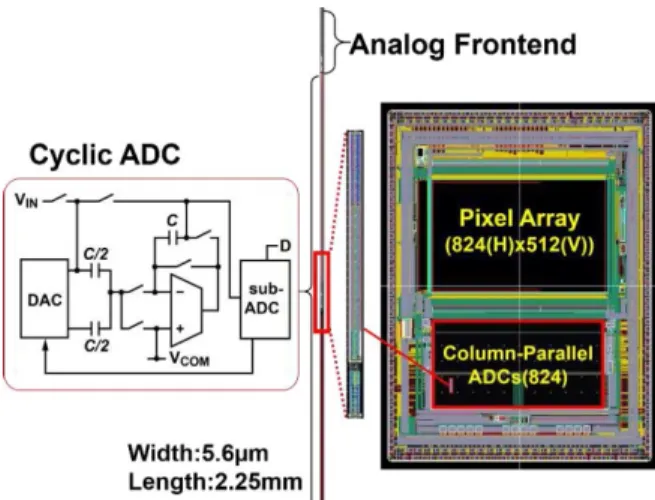
“ANALOG” to “DIGITAL” in imaging semiconductor de- vices. Current CMOS image sensors often use an image signal readout architecture using column-parallel analog- to-digital converters (ADCs)[1]–[78]. The column-parallel ADC allows us to read out image signals from the pixel ar- ray with less noise and higher bandwidth (or higher pixel rate) to process them with on-chip sophisticated digital im- age processing circuits and to transfer the image data to outside at very high pixel rate with no degradation of sig- nal quality. In CCD image sensors which use analog sig- nal readout from the chip meeting high bandwidth and low noise simultaneously is the most difficult task. Because the column-parallel ADC is a key element for CISs the performance of CISs is often dominated by the architec- tural choice of the column-parallel ADC. Figure 1 shows an example of layout pattern of a CIS and a column-parallel cyclic ADC used in the CIS chip. To implement the ADC at the column of fine-pitched pixel array of the CIS, the ADC elements must be embedded into the narrow column (e.g.,
Manuscript received February 5, 2018.
Manuscript revised March 27, 2018.
†The author is with Research Institute of Electronics, Shizuoka University, Hamamatsu-shi, 432–8011 Japan.
a) E-mail: [email protected] DOI: 10.1587/transele.E101.C.444
Fig. 1 CMOS Image Sensor and a column-parallel ADC.
width of 5.6µm in Fig. 1) and arranged as an array of many elements (e.g., 824 elements in Fig. 1). The ensemble of all the ADC elements provides very high image data rate for the image signal readout while maintaining the speed (band- width) of the ADC operation at each column to be very low.
The overall performance of designed CISs is maximized by exploiting these features of column-parallel ADCs. At the same time, the choice of the column-parallel ADC and the design of it must be carefully done because the ADC must be designed under very sever constraints due to the fine col- umn pitch.
The aim of this paper is to review architectures and topologies for column-parallel ADCs reported and discuss how the right ADC type is chosen depending on the specifi- cation of the CISs. To do this, new models for evaluating the column-parallel ADC performance are proposed and figures of merit (FoM) based on the models are defined. The valid- ity of the FoM defined are examined by applying the FoM to the performance data of CISs reported.
2. CMOS Image Sensors and Requirements for Column-Parallel ADCs
2.1 CIS Architecture
A typical block diagram of CISs is shown in Fig. 2 (a). A column-parallel ADC, a 1-D array with many ADC ele- ments is placed at the bottom of the pixel array. Each ADC element receives a pixel output signal through a vertical sig- nal line and converts the analog signal to a digital signal at Copyright c2018 The Institute of Electronics, Information and Communication Engineers
Fig. 2 CIS, column-parallel ADC, and operation timing.
the front-end part of the column readout circuits. A typ- ical pixel diagram of CISs is shown in Fig. 2 (b). The CIS pixel consists of a pinned photodiode and 4 transistors for an amplifier (source follower), resetting, selecting and charge transferring. The signal readout timing diagram is shown in Fig. 2 (c). One readout cycle of reading a set of pixels for thei-th row consists of (1) selecting the pixel (SL(i):High), (2) resetting the charge sensing node (RT(i):High), (3) sam- pling and A/D conversion for the reset level of the pixel output, (4) photo-charge transfer from a photodiode to the charge sensing node (TX:High), (5) sampling and A/D
conversion for the photo-signal level of the pixel output, and (6) digital correlated double sampling (CDS) for pixel noise cancelling. The image data for each column is once stored in a memory and the data is scanned horizontally in the time slot of the next readout cycle for reading the data of one row to the outside of the sensor chip.
2.2 Requirements for Column-Parallel ADC
In CMOS image sensors withNv(# of vertical pixels) xNH
(# of horizontal pixels) pixels, the readout cycle time of one row,THis given by
TH= 1 NV(1+rVO)ff
(1) whererVOis the factor of blanking time for vertical header codes and vertical optical black andffis the frame rate. The pixel rate, which is the required rate of reading all the pixels within a given frame rate is expressed as
Rp=NHNV(1+rVO)(1+rHO)ff (2) where rHO is the factor of blanking time for horizontal header codes and horizontal optical black. If each pixel has anNB-bit gray-scale levels usingNB-bit A/D conversion, the output bit rate is given by
Rb=NBNHNV(1+rVO)(1+rHO)ff (3) In Table 1, typical values of TH, Rp, and Rb in high- definition video imaging is summarized. Never-ending de- mands for better quality and reality in imaging require im- age sensors and column-parallel ADCs with extreme per- formances. For instance, in full-spec 8K image sensors with the frame rate of 120fps, one horizontal readout cycle time of<2µs is required and the time for A/D conversion in the column ADC must be<1µs if two times of the A/D conver- sion are carried out for the digital CDS. Special demands for slow-motion playback in 8K featuring a frame rate of 480fps requires further faster A/D conversion. The choice of ADC architecture, circuit topology for that and design effort are very important task for the developments of image sensors with these extreme specifications.
2.3 Technology Factors Relevant to the Evaluation of CISs and Column-Parallel ADCs
Recent progress of CIS process and device technology
greatly improve the performance of CISs, and it influences the architectural choice of the column parallel ADCs. For the performance evaluation of a column-parallel ADC and the CIS using it, knowing what process/device technology factors are used is necessary in order to examine the rea- son of the improvements. These technology factors are as follows:
[A] Process Node
A fine process technology contributes to the perfor- mance of the CIS and column-parallel ADC, particularly for low-power consumption in digital-rich types of ADCs.
[B] Backside Illumination (BSI)
For attaining high quantum efficiency in CISs with fine pixel pitch, backside illumination (BSI) structures have been introduced since around the middle of 2000s. The BSI can contribute not only to enhance the sensitivity but also to im- prove the interconnection capability between the pixel array and the peripheral circuit area. This is because the BSI al- lows to use all the areas on top of pixels for the interconnec- tions. This greatly helps to improve the CIS performance if high pixel rate is required.
[C] 3D Stacking
3D stacking technology introduced since around the beginning of 2010s, of course, greatly contributes to the per- formance improvements of CISs. The 3D stacking of a sen- sor layer and processing circuit layer allows us to attain ef- ficient interconnections between the pixels and the column- parallel ADCs and also between the column-parallel ADCs and the processing circuits. Based on the 3D stacking, the major architecture of ADC may change from column par- allel to pixel parallel in near future, and actually CISs with pixel-parallel ADCs with excellent performances have been reported[80]. In this paper, however, discussion is focused only on CISs using column-parallel ADCs.
[D] Global Shutter
Developments of global-shutter CISs are becoming ac- tive recently. In the case of conventional rolling-shutter CISs, the architecture for reading pixel signals to the pe- ripheral circuit area cannot be flexibly changed because of changing the order of reading pixel signals may cause a mo- tion artifact. The use of global-shutter pixel may contribute to a flexible and efficient pixel signal readout architecture and a better resulting performance of CISs.
3. Architectures of Column-Parallel ADCs
Many different architectures and circuit topologies for column-parallel ADCs have been reported. The major ar- chitectures are categorized into 4 types; (a) single-slope ADC, (b) successive approximation ADC, (c) algorithmic- or cycle-based ADC, and (d) delta-sigma modulation ADC.
In addition to these, recent CISs often employs column- parallel ADCs with extended intrascene dynamic range. In this section, principle, operation and feature of the typical column-parallel ADCs are reviewed.
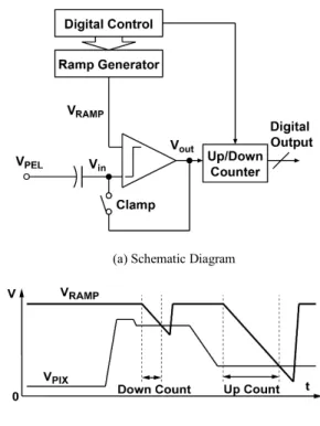
Fig. 3 Single-slope ADC for digital CDS using an up/down counter.
3.1 Single-Slope ADC
Figure 3 shows a typical single-slope ADC (SS-ADC) for column implementation[2], [9]. Single-slope ADCs are very popular for a column-parallel ADC in CISs because of its very simple circuit configuration and good linearity.
At each column, a comparator and up-down counter only are necessary. The ramp-signal generator is common for all the columns. A ramp signal is applied two times for re- set level and signal level as shown in Fig. 3 (b) and the two single-slope A/D conversions for the reset and signal lev- els are carried out by an up-counting and down-counting, respectively, using an up-down counter to perform a digital CDS so that the resulting output is the difference of them.
The time of the NB-bit single-slope A/D conversion TADC,SSfor the signal level using a counting clock frequency of fCKis given by
TADC,SS= 2NB+CCDS
fCK
(4) where CCDSis a counting margin for doing the digital CDS.
In the SS-ADC, the A/D conversion time for the reset level can be very small when compared with that for the sig- nal level. To do this, auto-zeroing technique is used in the comparator as shown in Fig. 3 (b) to cancel the fixed pattern noise component of the reset level. Since the A/D conver- sion time of the SS-ADC is proportional to the exponential ofNB, a relatively long time is necessary particularly if high gray-scale resolution is required. In order to use the SS- ADC for a high-definition 12-bit CIS, a technique using very high counting clock is developed. In the 17.7Mpixel 120fps
Fig. 4 DAC and Comparator for 14-bit SAR ADC for column imple- mentation.
12b CIS[17], the counting clock frequency of 2.376GHz is used and 12-bit A/D conversion time of 1.72µs and TH of 7.4µs are attained.
In CISs using the SS-ADC, a comparator is an only analog component used at a column, and the power con- sumption of the CISs using the SS-ADC is believed to be relatively low. However, if high speed and highNB are re- quired, it should be also noted that the ramp-signal gener- ator for delivering accurate ramp signal to all the columns and counters with high-frequency clocks consumes pretty large power. For faster and reduced counter clock frequency in single-slope ADCs, many two-step approaches have been investigated[12]–[14],[16]. Extra carefulness is necessary to use the two-step conversion if a good linearity compara- ble to the single-step single-slope ADC.
3.2 Successive Approximation ADC
A successive approximation ADC, or successive approxi- mation register ADC (SAR-ADC) is useful as a column ADC if high-speed operation is required. SAR-ADCs using a capacitor-array DAC are widely used. A possible prob- lem of the SAR-ADC is that large area is occupied by the capacitor-array DAC if high NB is required. A technique to cope with this problem as shown in Fig. 4 is developed for a column-parallel 14-bit SAR-ADC[33]. In a straight- forward 14-bit DAC, the ratio of maximum to minimum ca- pacitances is 213 : 1 and if the minimum unit capacitance is C0, the total of 214elements each of which isC0are neces- sary. The DAC in Fig. 4 uses three reference voltages, and by applying smaller reference voltages (1/22 and 1/24 of the largest reference voltage) to the LSB sides of operation, the maximum/minimum capacitor ratio is relaxed to 29 : 1, and this reduces the area required for the DAC to be 1/24 of the straight-forward case if the sameC0is used. The col- umn SAR ADC consumes relatively low power because the comparator is an only component that consumes DC power in the column while attaining relatively fast conversion be- causeNB-bit A/D conversion is done byNBsteps.
In the column SAR-ADC, complicated switching cir-
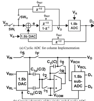
Fig. 5 Cyclic-based ADCs for column Implementation.
cuits for the capacitor-array DAC must be implemented at the narrow column and very careful layout design is neces- sary for attaining specified linearity.
3.3 Cyclic ADC and Cyclic-based Pipelined ADC For faster and higher NB, the cyclic ADC or also called an algorithmic ADC is also a useful architecture for column ADCs. Though cyclic ADCs were recognized to be com- plicated circuits, a very-simplified cyclic ADC using the single-ended integrator-based circuits as shown in Fig. 5 (a) and (b) has been introduced[58]and it allows us to use the cyclic ADCs in a relatively narrow ADC array pitch[66]. A cyclic ADC consists of a low-resolution ADC (sub-ADC) whose digital outputs drive a low-resolution DAC to give a quantized analog estimate of the input. This DAC output is then subtracted from the input, which is amplified by gain of 2, to give a residue. The ideal relationship of the output of thei-th cycle and that of the previous cycle is given by.
Vo(i)=2Vo(i−1)−DC(i)VR (5) whereDC(i)∈ {−1,0,1}, (i=0,1, . . . ,N−1) is the 1.5-bit code of thei-th cycle andVRis the reference voltage which gives the full analog scale level of the ADC. The operation of the 1.5-bit ADC to produceDC(i) is described as
DC(i)=⎧⎪⎪⎪⎨
⎪⎪⎪⎩
1 (Vo(i)≥VR/4) 0 (−VR/4<Vo(i)<VR/4)
−1 (Vo(i)≤ −VR/4) . (6) At the first cycle, an analog input signal (VIN) is given at the input by turning SWI on (see Fig. 5 (a)), i. e.,Vo(0) =VIN., and since the second cycle, the integrator output is sampled and fed back to the input by turning SWO on to perform
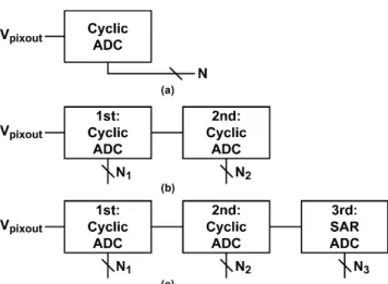
Fig. 6 Variations for Pipelined Multi-Stage Cyclic-based ADC
the cyclic or algorithmic A/D conversion given by Eq. (5).
In this 1.5-bit cyclic ADC,NB−1 cycles give the resolu- tion ofNB bits. Because of the gain of two at each cycle, the influence of the analog errors at latter cycles are re- laxed. These property allows us to implement a high-speed column ADC with high resolution. For power-efficient de- sign of the column cyclic ADC, the NB-bit cyclic ADC is divided into two cyclic ADC stages for the formerN1 cy- cles and latterN2cycles whereN1+N2 =NB−1 as shown in Fig. 6 (b). These two stages are operated in a pipelined fashion by extending over the 2nd-stage conversion into the next horizontal readout cycle of the CISs. This technique effectively reduces the sampling rate of the ADC analog cores. The 2nd cyclic ADC stage receives the residue out- put of the 1stcyclic ADC where the gain of 2N1is applied.
This greatly relaxes the tolerance to the analog errors in the 2nd stage and allows us to design a power-efficient ADC with high sampling rate. This two-stage pipelined cyclic ADC is applied to a 1.3Mpixel 2000fps 12-bit CIS[61]and 33Mpixel 120fps 12-bit/14-bit CISs[65],[69]and extreme performances in high-speed camera and 8K broadcasting camera have been demonstrated. In the 12-bit CIS, the di- vision into two cyclic ADCs to perform the first 4 cycles and the latter 8 cycles is the best of choice for the optimiza- tion of power efficiency, and the power efficiency of the de- signed two-stage cyclic ADC is 2.5-times better than that of the single-stage cyclic ADC. By dividing the cyclic-based ADC into three stages each of which is a low-resolution ADC and operating these in a pipelined fashion as shown in Fig. 6 (c), further power-efficient high-sampling rate de- sign of the column ADC is possible. In this case, since the last low-resolution ADC stage does not need to gener- ate an analog residue, a power-efficient SAR-ADC is used.
This three-stage (Cyclic-Cyclic-SAR) ADC is applied to a 33Mpixel 240fps 12-bit CIS for 8K cameras with a function of slow-motion playback[71].
Fig. 7 Adaptive-Gain Amplification for Extended Dynamic Range
3.4 Column-Parallel ADCs for Extended Intrascene Dy- namic Range
Noise reduction is one of the most important functions in readout circuits for CMOS image sensors. The input- referred noise of CMOS image sensors can be reduced by high-gain amplification at the frontend of readout circuits.
However, the frontend amplification with high gain for noise reduction was conventionally done at the cost of reduced dy- namic range. Recently, many techniques for noise reduction while maintaining the intrascene dynamic range have been reported. Adaptive-gain amplification as shown in Fig. 7 is one of effective ways for low-noise extended dynamic range CISs[23],[78]. The gain is given by C1/C2. In Fig. 7 (a), the pixel output is first compared with a given threshold of VTand if the amplitude is smaller thanVT, large gain of 8, for instance, is used by setting C2 = C1/8. If the ampli- tude is larger than VT, the gain of unity is used by setting C2 =C1. IfVT is chosen as 1/8 or a little smaller than the analog maximum range of the column ADC, a large gain of 8 is adaptively used for small amplitude pixel signal without saturating at the ADC input for an incidental large ampli- tude pixel signal. In Fig. 7 (b), the gain adaptation is done by looking at the amplifier output when the gain is set to high. If the amplitude of the amplifier output is larger than the thresholdVT, the amplifier output is limited by a limiting circuit (not shown in Fig. 7 (b)), and the gain of the amplifier is reset to unity.
There are a few other techniques for the column- parallel ADC with noise reduction while maintaining the in- trascene dynamic range. A pseudo multiple sampling tech- nique using a single-slope ADC samples the pixel output many times and averages their ADC outputs to produce a noise-reduced resolution-increased digital signal[15]. A dual-gain A/D conversion using a single-slope ADC and two slope gains to the same pixel output is also a simple and
Fig. 8 2nd-Order Delta-Sigma ADC for column Implementation.
effective technique for obtaining reduced noise and ex- tended intrascene dynamic range at relatively high pixel rate[20].
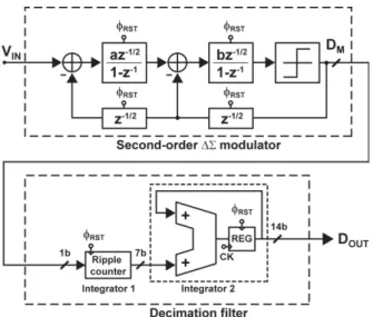
3.5 Delta-Sigma Modulation ADC
A/D Converters using over-sampling techniques are also very useful for column ADCs with noise reduction and ex- tended dynamic range. A 2nd-order incremental delta-sigma modulator ADC as shown in Fig. 8 is of a reasonable choice because of the balance between the circuit complexity and the efficiency for noise shaping to obtain high gray-scale resolution[68]. In this type of circuits, the oversampling and low-pass filtering effect by the decimation filter has an effect of white noise reduction and an effect for extended dynamic range is self-contained. An issue for this 2nd- order delta-sigma modulator is that it requires many sam- pling clock cycles if very high bit-resolution is required. The bit-resolution,NBis determined by the number of sampling clock cycles,Mas follows:
NB=log2 M(M+1)
2 [bit] (7)
ForNB of 12, 14 and 16 bits, M of 90, 181 and 362 are required, respectively.
For more efficiently obtaining high bit-resolution with smaller number of sampling clock cycles, an ADC tech- nique using 1st-order incremental delta-sigma modulator shown in Fig. 9 can be used. In this ADC, the first step for the 1st-order incremental delta-sigma modulation is done for the input withMsampling clock cycles and the second step for the residue output (integrator output)ROUT in Fig. 9 is done by anotherNB2-bit A/D converter. This type of A/D conversion is called an extended counting ADC[81]. The author calls this technique the folding-integration ADC[74]
if this is used as a column-parallel ADC of CISs because the value of this ADC as used at the column of image sensors is due to the efficient noise reduction effect of the analog
Fig. 9 First-order Incremental Delta-Sigma Modulator for Folding Inte- gration (or Extended Counting).
integrator used in the delta-sigma modulation with multi- ple sampling of the input and the folding effect to maintain the amplitude of the integrator within an analog range de- termined by a amplitude of the 1-bit DAC. As a result, this ADC has an efficient noise reduction effect for both thermal noise and 1/f noise of in–pixel source-follower amplifiers and peripheral readout circuits while extending the dynamic range[83]. In this ADC, the bit-resolution is given by
NB=log2 M
2 +NB2[bit]. (8)
With the help of a high-resolution ADC for the residue out- put, a very high-resolution column-parallel ADC is realized with smaller number of sampling clock cycles for the input.
In the CIS chip using this ADC with 13-bit cyclic ADC for the residue output, maximally 19-bit resolution usingMof 128[73] and 17b DNL of+1.4LSB/−0.9LSB using M of 32[75]has been demonstrated.
4. Definition of Figures of Merit of CMOS Image Sen- sors with Column-Parallel ADCs
For performance evaluation of CMOS image sensors using column-parallel ADCs, figures-of-merit (FoM) calculated with their specification and attained performance are useful.
Though the aim of calculating the FoM is to evaluate mainly the performance of the column-parallel ADC, the merit of image sensor’s entire performance is considered. The fol- lowing FoM considering noise, power dissipation, and pixel rate is often used[85].
FoM1= Noise×Power
Rp ×109[e−·nJ] (9) This FoM is useful for evaluating the performance of CISs if the power dissipation is proportional to the pixel rate and the noise is controlled independent of the pixel rate. How- ever, such an assumption is not always met particularly if the pixel rate is very high and the dominant noise is thermal noise or other noise whose spectrum is spreading to high- frequency range.
FoM of more reflecting the noise behavior of CISs is defined here. The power consumption of CISs is mainly the sum of those of the pixel array, front-end amplifier if used, column ADC, column logic and I/O. All these components’
power consumption can be considered to be proportional to the horizontal pixel number, vertical pixel number and frame rate, i.e., their product or the pixel rate. Among the above, analog readout circuits like a front-end amplifier and column ADC are designed for reducing the power by optimizing the capacitor sizeCTused for these analog circuits at the cost of thermal noise increase. Therefore, the power consumption of CISs is expressed as
Power=K1Rp+K2CTRp (10) whereK1andK2are proportional constants.
The behavior of noise in CISs is complicated. If the pixel rate is low enough and the thermal or white noise components of the readout noise is controlled to be very low by using bandwidth limitation techniques, and then the temporal readout noise is dominated by 1/f noise of MOS transistors of the in-pixel source follower and it can be re- garded as independent of the pixel rate. However, if the pixel rate is relatively high, the signal bandwidth becomes higher and thermal noise due to MOS transistors used in the analog readout circuits may dominate. The thermal noise is band-limited by capacitors used for the analog readout cir- cuits and the noise power or mean squared noiseVn,T2 is observed as a form ofK3(kT/CT) where K3 is a constant, kthe Boltzmann constant,T the absolute temperature and CT the capacitance for bandwidth limitation. In very high pixel rate, for instance, which is required for full-spec 8K image sensors, other noise components may dominate the noise level. In CISs with column-parallel readout channels, the bandwidth is related to one readout cycle time of one row and the noise power if the noise source is white noise is expressed as
Vn,S2=K4SN
1
TH K4SNNVff (11) whereSN is the noise power spectrum density per unit fre- quency andK4 is the proportional constant. In high pixel- rate image sensors of which the horizontal data scanning is done with a pipelined fashion as shown in Fig. 2 (c), one can assume that the dominant noise source is due to switching noise caused by high-speed digital data scanning and read- ing to the outside of the sensor chip. If such a noise source at each column is independent, or there is no noise correlations between columns, an assumption that the noise power spec- trum density is assumed to be the sum of each noise power spectrum generated at each column and is proportional to the number of columnsNH, i. e.,
SN =K5NH (12)
whereK5is a proportional constant. Then the noise power is given by
Vn,S2 K4K5NHNVff =K6Rp (13) whereK6is a proportional constant. By taking all the noise components into account, a general form of the CIS noise is expressed as
Vn2K3
kT
CT +Vn,F2+K6Rp (14) whereVn,F2is the mean squared noise mainly due to pixel’s 1/f noise components of MOS transistors. In a situation that thermal noise dominates and the power dissipation is opti- mized for reducing thermal noise of amplifiers, the product of the mean squared noise (Eq. (14)) and power (Eq. (12)) is approximated as
Vn2×PowerK3kT CT
×K2CTRp=K7RP (15) whereK7is a proportional constant. At low pixel rate, if the pixel 1/f noise dominates, the squared noise-power product is expressed as
Vn2×PowerVn,F2×(K1Rp+K2CTRp)=K8RP (16) where K8 is a proportional constant. The situations of Eq. (16) and Eq. (15) are met for low and relatively-high pixel-rate CISs, respectively. At very high pixel rate where the digital-system noise dominates, the mean squared noise- power product is expressed as
Vn2×PowerK6Rp×(K1Rp+K2CTRp)=K9RP2 (17) where K9 is a proportional constant. These observations suggest us a new definition of FoM. For the pixel rate below Rpc where Rpc is the corner pixel rate for the FoM model change, the FoM given by
FoM2L= Noise2×Power Rp
×109[(e−)2·nJ] (18) should be used and if the CIS is evaluating at high pixel rate (>Rpc), the FoM defined as
FoM2H=Noise2×Power
Rp2 ×109[(e−)2·nJ/GHz] (19) should be used.
If attaining high intrascene dynamic range (IDR) valu- able for CISs, an FoM defined as
FoM3L= Noise×Power
IDR×Rp ×1012[e−·pJ/DRU] (20) should be used if the pixel rate is not very high, where DRU (dynamic range unit) is a unit of calculating theIDRgiven by
IDR= SignalMax/AG
Noise [DRU] (21)
where SignalMax is the maximum signal amplitude ex- pressed as the number of electrons, and AG is the analog gain applied to attain the best of noise. The division byAG to calculate theIDRis because applying the analog gain of AGto reduce the noise in front of A/D conversion reduces theIDRby a factor ofAG. If a technique for extending the IDR is used and the input-referred signal amplitude is main- tained even if an analog gainAGis applied, the AG should
should be used instead of Eq. (20). The definition of the FoM in Eq. (20) is quite similar to the FoM used for eval- uating stand-alone ADCs[84]where the FoM is defined as an idea that (DynamicRange)2×(Power)/(Bandwidth) of the ADC is constant if the ADC is designed by the same archi- tecture, topology, and technology[84].
Another FoM considering the merit of high gray-scale resolution column ADC can be defined by the analogy from Eq. (20) as
FoM4=Noise×Power ADR×Rp
×1012[e−·pJ/Conv.-step]
(23) whereADRis the ADC code range and the conversion-step is a minimum step of the gray-scale levels. If an NB-bit column ADC is implemented in the CIS,ADR =2NB (and the conversion-step=1LSB) is used here.
5. FoM-Based Performance Evaluation of Column- Parallel ADCs for CISs
In order to check the validity of FoM defined in Sect. 4 and to evaluate the performance of column-parallel ADCs used in the actually implemented CISs, performance data of CISs papers presented and published at major interna- tional conferences (Int. Solid-State Circuits Conf. (ISSCC), VLSI Circuits Symp., Int. Image Sensor Workshop (IISW), European Solid-State Circ. Conf. (ESSCIRC)) and interna- tional journals (IEEE J. Solid-State Circ., IEEE Trans. Elec- tron Devices, MDPI Sensors) are surveyed. CISs which em- ploy column-parallel ADCs are picked up. The column- parallel ADCs are categorized into 4types, i.e., “Single- Slope”[1]–[24], “SAR”[25]–[42], “Cyclic”[43]–[66], and
“Delta-Sigma”[67]–[78]. The group of ADCs using the 1st- order incremental delta sigma modulator and extended con- version for the residue output[73]–[78]is categorized in the
“Delta-Sigma”.
Figure 10 shows the noise versus pixel rate of CISs re- ported. Recently, techniques for extremely-low-noise CISs whose noise level is below 0.5e- have been reported. How- ever, most of those are demonstrated with experimentally- implemented CIS chips, or quanta CIS using 1-bit ADC ex- cept for Ref.[78]. By excluding Ref.[78], one can observe that the front-line of noise level in low-noise CISs is around 1e- and it is constant up to the pixel rate of 600 to 700MHz.
At very high pixel rate, as suggested by the model described in Sect. 4, attaining very low noise becomes difficult because
Fig. 10 Noise versus pixel rate plot of CISs reported
Fig. 11 Plot for common FoM (noise·power versus pixel rate).
of the noise generation due to high-speed digital signal read- out which is done at the background of analog readout pro- cessing. According to Eq. (13), the noise is proportional to Rp in this region and this model looks valid in the pixel rate of above 700MHz in Fig. 10.
Figure 11 shows a plot for the evaluation based on the FoM commonly used, i.e., the plot of (noise)x(power) ver- sus (pixel rate). The diagonal line showsFoM1 defined in Eq. (9). The front-line of the best FoM in this definition is currently around 1.0 [e- nJ]. This FoM looks valid for rough observation of the progress of CIS technology because the best FoM at different pixel rates are well aligned in the line for the FoM1.
Figure 12 shows a plot of (noise)2x(power) versus (pixel rate). The diagonal line in the region of pixel rate of<
700MHz showsFoM2Ldefined in Eq. (18). The front-line of the best FoM in this definition is currently around 1.5 [(e-)2 nJ] due to the development of CISs of Ref.[23] reported in 2017 which uses a global shutter pixel and dual-gain amplified single-slope ADC and Ref.[20]reported in 2015 which uses BSI, 3D-Stacking, and a single-slope ADC. Be-
Fig. 12 Plot for FoM2 (noise2·power versus pixel rate).
Fig. 13 Plot for FoM3 (noise·power/intrascene-DR versus pixel rate).
fore these development, the front-line looks around 4 [(e-)2 nJ]. For higher pixel-rate region (∼>1000MHz), theFoM2H
defined in Eq. (19) well explains the front line if a CIS us- ing BSI, 3D-Stacking and a 3-Stage pipelined cyclic-based ADC in Ref.[66]is excluded.
Figure 13 shows a plot of (noise) x (power)/(intrascene dynamic range) versus (pixel rate). The diagonal line in the region of pixel rate of<700MHz showsFoM3L defined in Eq. (20). The frontline of the best FoM in this definition is currently around 0.25 [e- pJ/DRU], and the CISs of Ref.[23]
using dual-gain adaptive amplification and Ref.[68]using incremental 2nd-order Delta-Sigma ADC are on the front- line. The data of Ref.[24]is obtained by the same CIS chip in Ref.[23]. Because it is not clear the reason why two- times better FoM than that in Ref.[23]is obtained in spite of using the same chip and same operation, the data point of Ref.[24]is once excluded in the discussion here. For higher pixel-rate region (∼>1000MHz), theFoM3Hdefined in Eq. (22) well explains the frontline. In this region, the CIS
Fig. 14 Plot for FoM4 (noise·power/gray-scale-range versus pixel rate)
of Ref.[20]using a global shutter, 3D-stacking at periph- eral area, and adaptive dual-slope ADC is on the frontline.
The CIS in Ref.[66]using BSI, 3D-stacking and a 3-stage pipelined cyclic-based ADC is also on the frontline. From these observation, we can conclude that column ADC archi- tectures using techniques for extending dynamic range de- scribed in Sect. 3 are all successful for attaining totally well- balanced high performance considering factors of low noise, low power dissipation, high dynamic range, high frame rate and high resolution (large pixel number).
Figure 14 shows a plot of (noise) x (power)/(ADC code range) versus (pixel rate). In this metrics, the value of ob- taining high gray-scale resolution is stressed and the CISs using 14-bit cyclic[64]and 17-bit delta-sigma[75] ADCs are on the frontline of this definition of FoM, i. e.,FoM4for the regions of both high and low pixel rates, respectively.
6. Conclusions
In this paper, column-parallel analog-to-digital converters for CMOS image sensors are reviewed and their perfor- mances are discussed using metrics calculated by figures of merit (FoM). Models for separately evaluating the perfor- mance of the CISs in low/middle and high pixel-rate regions are proposed and several FoM considering different perfor- mance factors are defined. The defined FoM are applied to surveyed data on CISs reported and the following conclu- sions are obtained:
- The performance of CISs should be evaluated with differ- ent metrics to high pixel-rate regions (∼>1000MHz) from those to low or middle pixel-rate regions.
- The conventional FoM (commonly-used FoM) calculated by (noise) x (power)/(pixel-rate) is useful for observing en- tirely the trend of performance frontline of CISs.
- The FoM calculated by (noise)2 x (power) /(pixel-rate) which considers a model on thermal noise and digital sys-
ing high gray-scale resolution, and cyclic-based and delta- sigma ADCs are on the frontline for high and low pixel-rate regions, respectively.
Acknowledgments
This work was supported in part by the Japan Society for the Promotion of Science (JSPS) KAKENHI, the Grant-in Aid for Scientific Research (S) under Grant 25220905, the Grant-in-Aid for Scientific Research on Innovative Area, 25109003, in part by the MEXT/JST COI-STREAM pro- gram, in part by the MEXT Regional-Innovation Ecosystem program. The author would like to thank Dr. De Xing Lioe, Dr. Keita Yasutomi and Dr. Min-Woong Seo of Shizuoka University for helpful discussion.
References
[1] K. Chen, M. Afghani, P.E. Danielsson, and C. Svensson, “PASIC: A processor-A/D converter-sensor integrated circuit,” IEEE Int. Symp.
Circ. and Syst., New Orleans, LA, vol.3, pp.1705–1708, 1990.
[2] W. Yang, O.-B. Kwon, J.-I. Lee, G.-T. Hwang, and S.-J. Lee, “An in- tegrated 800x600 CMOS imaging system,” Dig. Tech. Papers, IEEE Int. Solid-State Circuits Conf. (ISSCC), pp.304–305, 1999.
[3] T. Sugiki, S. Ohsawa, H. Miura, M. Sasaki, N. Nakamura, I. Inoue, M. Hoshino, Y. Tomizawa, and T. Arakawa, “A 60 mW 10 b CMOS image sensor with column-to-column FPN reduction,” Dig. Tech.
Papers, IEEE ISSCC, pp.108–109, 2000.
[4] A. Krymski, N. Khaliullin, and H. Rhodes, “A 2 e− Noise 13 Megapixel CMOS Sensor,” Proc. IEEE Workshop CCD and Ad- vanced Image Sensors, pp.15–17, May 2003.
[5] K. Findlater, R. Henderson, D. Baxter, J.E.D. Hurwitz, L. Grant, Y. Cazaux, F. Roy, D. Herault, and Y. Marcellier, “SXGA pinned photodiode CMOS image sensor in 0.35um technology,” Dig. Tech.
Papers, IEEE ISSCC, San Francisco, pp.218–489, 2003.
[6] M.F. Snoeij, A.J.P. Theuwissen, and J.H. Huijsing, “A 1.8 V 3.2µW comparator for use in a CMOS imager column-level single-slope ADC,” IEEE Int. Symp. Circ. and Syst., vol.6, pp.6162–6165, 2005.
[7] L. Lindgren, J. Melander, R. Johansson, and B. Moller, “A multires- olution 100-GOPS 4-Gpixels/s programmable smart vision sensor for multisense imaging,” IEEE J. Solid-State Circuits, vol.40, no.6, pp.1350–1359, June 2005.
[8] T. Otaka, Y. Lee, T. Bales, P. Smith, J. MacDowell, S. Smith, and I. Takayanagi, “12-Bit Column-Parallel ADC with Accelerated Ramp,” Prog. IEEE Workshop Charge-Coupled Devices Adv. Image Sensors, Nagano, Japan, pp.173–176, June 2005.
[9] S. Yoshihara, M. Kikuchi, Y. Ito, Y. Inada, S. Kuramochi, H.
Wakabayashi, M. Okano, K. Koseki, H. Kuriyama, J. Inutsuka, A.
Tajima, T. Nakajima, Y. Kudoh, F. Koga, Y. Kasagi, S. Watanabe, and T. Nomoto, “A 1/1.8-inch 6.4MPixel 60 frames/s CMOS Image Sensor with Seamless Mode Change,” Dig. Tech. Papers, IEEE Int.
Solid-State Circ. Conf., San Francisco, CA, pp.1984–1993, 2006.
[10] S. Yoshihara, Y. Nitta, M. Kikuchi, K. Koseki, Y. Ito, Y. Inada, S.
Kuramochi, H. Wakabayashi, M. Okano, H. Kuriyama, J. Inutsuka, A. Tajima, T. Nakajima, Y. Kudoh, F. Koga, Y. Kasagi, S. Watanabe,
[12] M.F. Snoeij, P. Donegan, A.J.P. Theuwissen, K.A.A. Makinwa, and J.H. Huijsing, “A CMOS Image Sensor with a Column-Level Mul- tiple-Ramp Single-Slope ADC,” Dig. Tech. Papers, IEEE Int. Solid- State Circ. Conf., San Francisco, CA, pp.506–507, 2007.
[13] M.F. Snoeij, A.J.P. Theuwissen, K.A.A. Makinwa, and J.H.
Huijsing, “Multiple-Ramp Column-Parallel ADC Architectures for CMOS Image Sensors,” IEEE J. Solid-State Circuits, vol.42, no.12, pp.2968–2977, Dec. 2007.
[14] S. Lim, J. Lee, D. Kim, and G. Han, “A High-Speed CMOS Image Sensor With Column-Parallel Two-Step Single-Slope ADCs,” IEEE Trans. Electron Devices, vol.56, no.3, pp.393–398, March 2009.
[15] Y. Lim, K. Koh, K. Kim, H. Yang, J. Kim, Y. Jeong, S. Lee, H.
Lee, S.-H. Lim, Y. Han, J. Kim, J. Yun, S. Ham, and Y.-T. Lee, “A 1.1e- temporal noise 1/3.2-inch 8Mpixel CMOS image sensor using pseudo-multiple sampling,” Dig. Tech. Papers, IEEE Int. Solid-State Circ. Conf., San Francisco, pp.396–397, 2010.
[16] T. Takahashi, H. Ui, N. Takatori, S. Sanada, T. Hamamoto, H.
Nakayama, Y. Moriyama, M. Akahide, T. Ueno, and N. Fukushima,
“A Digital CDS Scheme on Fully Column-Inline TDC Architecture for An APS-C Format CMOS Image Sensor,” Tech. Dig., Symp.
VLSI Circ., pp.90–91, 2011.
[17] T. Toyama, K. Mishina, H. Tsuchiya, T. Ichikawa, H. Iwaki, Y.
Gendai, H. Murakami, K. Takamiya, H. Shiroshita, Y. Muramatsu, and T. Furusawa, “A 17.7Mpixel 120fps CMOS image sensor with 34.8Gb/s readout,” 2011 IEEE Int. Solid-State Circ. Conf., San Francisco, CA, pp.420–422, 2011.
[18] A. Suzuki, N. Shimamura, T. Kainuma, N. Kawazu, C. Okada, T.
Oka, K. Koiso, A. Masagaki, Y. Yagasaki, S. Gonoi, T. Ichikawa, M.
Mizuno, T. Sugioka, T. Morikawa, Y. Inada, and H. Wakabayashi,
“A 1/1.7-inch 20Mpixel Back-illuminated stacked CMOS image sensor for new imaging applications,” Tech. Dig., IEEE ISSCC, pp.1–3, 2015.
[19] Y. Oike et al., “An 8.3M-Pixel 480fps global-shutter CMOS image sensor with gain-adaptive column ADCs and 2-on-1 stacked device structure,” Symp. VLSI Circuits Dig. Tech. Papers, pp.222–223, June 2016.
[20] Y. Oike, K. Akiyama, L.D. Hung, W. Niitsuma, A. Kato, M. Sato, Y. Kato, W. Nakamura, H. Shiroshita, Y. Sakano, Y. Kitano, T.
Nakamura, T. Toyama, H. Iwamoto, and T. Ezaki, “8.3 M-Pixel 480-fps Global-Shutter CMOS Image Sensor with Gain-Adaptive Column ADCs and Chip-on-Chip Stacked Integration,” IEEE J.
Solid-State Circuits, vol.52, no.4, pp.985–993, April 2017.
[21] J. Bogaerts, R. Lafaille, M. Borremans, J. Guo, B. Ceulemans, G.
Meynants, N. Sarhangnejad, G. Arsinte, V. Statescu, and S. van der Groen, “105×65mm2 391Mpixel CMOS Image Sensor with>78dB Dynamic Range for Airborne Mapping Applications,” Tech. Dig., IEEE ISSCC, pp.113–114, 2016.
[22] H. Totsuka, T. Tsuboi, T. Muto, D. Yoshida, Y. Matsuno, M.
Ohmura, H. Takahashi, K. Sakurai, T. Ichikawa, H. Yuzurihara, and S. Inoue, “An APS-H-Size 250Mpixel CMOS Image Sensor Us- ing Column Single-Slope ADCs with Dual-Gain Amplifiers,” Tech.
Dig., IEEE ISSCC, pp.115–116, 2016.
[23] M. Kobayashi, Y. Onuki, K. Kawabata, H. Sekine, T. Tsuboi, Y.
Matsuno, H. Takahashi, T. Koizumi, K. Sakurai, H. Yuzurihara, S.
Inoue, and T. Ichikawa, “A 1.8erms Temporal Noise Over 110dB Dynamic Range 3.4µm Pixel Pitch Global Shutter CMOS Image Sensor with Dual-Gain Amplifiers, SS-ADC and Multiple-Accumu- lation Shutter,” Tech. Dig., IEEE ISSCC, pp.74–75, 2017.
[24] H. Sekine, M. Kobayashi, Y. Onuki, K. Kawabata, T. Tsuboi, Y. Matsuno, H. Takahashi, S. Inoue, and T. Ichikawa, “Global shutter CMOS image sensor with light guide structure,” Proc. IISW, pp.394–397, 2017.
[25] Z. Zhou, B. Pain, and E.R. Fossum, “CMOS active pixel sensor with on-chip successive approximation analog-to-digital converter,”
IEEE Trans. Electron Devices, vol.44, no.10, pp.1759–1763, 1997.
[26] B. Mansoorian, H.-Y. Yee, S. Huang, and E. Fossum, “A 250 mW, 60 frames/s 1280/spl times/720pixel 9b CMOS digital image sensor,”
Dig. Tech. Papers, IEEE Int. Solid-State Circ. Conf., pp.312–313, 1999.
[27] A. Krymski, D. Van Blerkom, A. Andersson, N. Bock, B.
Mansoorian, and E.R. Fossum, “A high speed, 500 frames/s, 1024x1024 CMOS active pixel sensor,” Tech. Dig, Symp. VLSI Circ., pp.137–138, 1999.
[28] A.I. Krymski and N. Tu, “A 9-V/lux-s 5000-frames/s 512 x 512 CMOS sensor,” IEEE Trans. Electron Devices, vol.50, no.1, pp.136–143, 2003.
[29] I. Takayanagi, M. Shirakawa, K. Mitani, M. Sugawara, S. Iversen, J. Moholt, J. Nakamura, and E.R. Fossum, “A 1-1/4 inch 8.3M Pixel Digital Output CMOS APS for UDTV Application,” Dig. Tech. Pa- pers, ISSCC, pp.216–217, 2003.
[30] I. Takayanagi, M. Shirakawa, K. Mitani, M. Sugawara, S. Iversen, J.
Moholt, J. Nakamura, and E.R. Fossum, “A 1.25-inch 60-frames/s 8.3-M-pixel digital-output CMOS image sensor,” IEEE J. Solid- State Circuits, vol.40, no.11, pp.2305–2314, Nov. 2005.
[31] A.I. Krymski, N.E. Bock, N. Tu, D. Van Blerkom, and E.R.
Fossum, “A high-speed, 240-frames/s, 4.1-Mpixel CMOS sensor,”
IEEE Trans. Electron Devices, vol.50, no.1, pp.130–135, Jan. 2003.
[32] S. Matsuo, T. Bales, M. Shoda, S. Osawa, B. Almond, Y. Mo, J.
Gleason, T. Chow, and I. Takayanagi, “A Very Low Column FPN and Row Temporal Noise 8.9 M-Pixel, 60 fps CMOS Image Sen- sor with 14bit Column Parallel SA-ADC,” Dig. Tech. Papers, Symp.
VLSI Circuits, pp.138–139, 2008.
[33] S. Matsuo, T.J. Bales, M. Shoda, S. Osawa, K. Kawamura, A.
Andersson, M. Haque, H. Honda, B. Almond, Y. Mo, J. Gleason, T. Chow, and I. Takayanagi, “8.9-Megapixel Video Image Sensor With 14-b Column-Parallel SA-ADC,” IEEE Trans. Electron De- vices, vol.56, no.11, pp.2380–2389, Nov. 2009.
[34] J. Solhusvik et al., “A 1280x960 3.75um pixel CMOS imager with Triple Exposure HDR,” Proc. Int. Image Sensor Workshop, pp.344–
347, 2009.
[35] M.-S. Shin, J.-B. Kim, M.-K. Kim, Y.-R. Jo, and O.-K. Kwon,
“A 1.92-Megapixel CMOS Image Sensor With Column-Parallel Low-Power and Area-Efficient SA-ADCs,” IEEE Trans. Electron Devices, vol.59, no.6, pp.1693–1700, June 2012.
[36] R. Xu, B. Liu, and J. Yuan, “A 1500 fps Highly Sensitive 256x256 CMOS Imaging Sensor With In-Pixel Calibration,” IEEE J. Solid- State Circuits, vol.47, no.6, pp.1408–1418, June 2012.
[37] H. Honda et al., “A 1-inch optical format, 14.2M-pixel, 80fps CMOS image sensor with a pipelined pixel reset and readout operation,”
2013 Symposium on VLSI Circuits, Kyoto, pp.C4–C5, 2013.
[38] D.G. Chen, F. Tang, and A. Bermak, “A Low-Power Pilot-DAC Based Column Parallel 8b SAR ADC With Forward Error Correc- tion for CMOS Image Sensors,” IEEE Trans. Circuits Syst. I, Reg.
Papers, vol.60, no.10, pp.2572–2583, Oct. 2013.
[39] R. Xu, W.C. Ng, J. Yuan, S. Yin, and S. Wei, “A 1/2.5 inch VGA 400 fps CMOS Image Sensor With High Sensitivity for Machine Vision,” IEEE J. Solid-State Circuits, vol.49, no.10, pp.2342–2351, Oct. 2014.
[40] Y.-R. Jo, S.-K. Hong, and O.-K. Kwon, “A Multi-Bit Incremental ADC Based on Successive Approximation for Low Noise and High Resolution Column-Parallel Readout Circuits,” IEEE Trans. Circuits Syst. I, Reg. Papers, vol.62, no.9, pp.2156–2166, Sept. 2015.
[41] R. Funatsu, S. Huang, T. Yamashita, K. Stevulak, J. Rysinski, D. Estrada, S. Yan, T. Soeno, T. Nakamura, T. Hayashida, H.
Shimamoto, and B. Mansoorian, “133Mpixel 60fps CMOS im-
age sensor with 32-column shared high-speed column-parallel SAR ADCs,” 2015 IEEE International Solid-State Circuits Conference - (ISSCC) Digest of Technical Papers, San Francisco, CA, pp.1–3, 2015.
[42] M.-K. Kim, S.-K. Hong, and O.-K. Kwon, “A fast multiple sampling method for low-noise CMOS image sensors with column-parallel 12-bit SAR ADCs,” Sensors, vol.16, no.1, pp.27–40, 2016.
[43] K. Chen and C. Svensson, “A parallel A/D converter array structure with common reference processing unit,” IEEE Trans. Circuits Syst, vol.36, no.8, pp.1115–1119, 1989.
[44] S. Tanner, A. Heubi, M. Ansorge, and F. Pellandini, “An 8-bit low-power ADC array for CMOS image sensors,” Proc. IEEE Int.
Conf. Elect. Circ. Sys., pp.147–150, 1998.
[45] S. Tanner, A. Heubi, M. Ansorge, and F. Pellandini, “A 8-bit low- power ADC array for CMOS image sensors,” Proc. ESSCIRC, 1998.
[46] S. Decker, R.D. McGrath, K. Brehmer, and C.G. Sodini, “A 256
×256 CMOS Imaging Array with Wide Dynamic Range Pixels and Column-Parallel Digital Output,” IEEE Int. Solid-State Circuits Conf. (ISSCC), pp.176–177, 1998.
[47] S. Decker, R.D. McGrath, K. Brehmer, and C.G. Sodini, “A 256× 256 CMOS Imaging Array with Wide Dynamic Range Pixels and Column-Parallel Digital Output,” IEEE J. Solid-State Circuits, vol.33, no.12, pp.2081–2091, 1998.
[48] T. Kato, S. Kawahito, K. Kobayashi, H. Sasaki, T. Eki, and T.
Hisanaga, “A binocular CMOS range image sensor with bit-serial block-parallel interface using cyclic pipelined ADC’s,” Tech. Dig., Symp. VLSI Circ., pp.270–271, 2002.
[49] D. Muthers and B. Tielert, “A 0.11mmˆ2 low-power A/D-converter cell for 10b 10MS/s operation,” Proc. ESSCIRC, 2004.
[50] M. Mase, S. Kawahito, M. Sasaki, and Y. Wakamori, “A 19.5b dy- namic range CMOS image sensor with 12b column-parallel cyclic A/D converters,” Tech., Dig., IEEE ISSCC, pp.350–351, 2005.
[51] M. Mase, S. Kawahito, M. Sasaki, Y. Wakamori, and M. Furuta,
“A wide dynamic range CMOS image sensor with multiple expo- sure-time signal outputs and 12-bit column-parallel cyclic A/D con- verters,” IEEE J. Solid-State Circuits, vol.40, no.12, pp.2787–2795, 2005.
[52] J.H. Park, M. Mase, S. Kawahito, M. Sasaki, Y. Wakamori, and Y.
Ohta, “A 142dB dynamic range CMOS image sensor with multiple- exposure time signals,” Proc. Asian Solid-State Circ. Conf., no.3-1, 2005.
[53] M. Furuta, S. Kawahito, T. Inoue, and Y. Nishikawa, “A cyclic A/D converter with pixel noise and column-wise offset cancelling for CMOS image sensors,” Proc. ESSCIRC, 2005.
[54] M. Furuta, T. Inoue, Y. Nishikawa, and S. Kawahito, “A 3500fps high-speed CMOS image sensor with 12b column-parallel cyclic A/D converter,” Tech. Dig., Symp. VLSI Circ., 2006.
[55] M. Furuta, Y. Nishikawa, T. Inoue, and S. Kawahito, “A high-speed, high-sensitivity digital CMOS image sensor with a global shutter and 12-bit column-parallel cyclic A/D converters,” IEEE J. Solid- State Circuits, vol.42, no.4, pp.766–774, 2007.
[56] S. Kawahito, J.-H. Park, K. Isobe, S. Suhaidi, T. Iida, and T.
Mizota, “A CMOS image sensor integrating column-parallel cyclic ADCs with on-chip digital error-correction circuits,” Dig. Tec. Pa- pers, IEEE ISSCC, pp.56–57, 2008.
[57] J.-H. Park, S. Aoyama, T. Watanabe, T. Akahori, T. Kosugi, K.
Isobe, Y. Kaneko, Z. Liu, K. Muramatsu, T. Matsuyama, and S.
Kawahito, “A 0.1e- vertical FPN 4.7e- read noise 71dB DR CMOS image sensor with 13b column-parallel single-ended cyclic ADCs,”
Tech. Dig., IEEE ISSCC, pp.268–269, 2009.
[58] J.-H. Park, S. Aoyama, T. Watanabe, K. Isobe, and S. Kawahito,
“A high-speed low noise CMOS image sensor with 13-b column- parallel single-ended cyclic ADCs,” IEEE Trans. Electron Devices, vol.56, no.11, pp.2414–2422, 2009.
[59] S. Lim, J. Cheon, Y. Chae, W. Jung, D. Lee, S. Ham, D. Kim, and G.
Han, “A 1/3.4-inch 2.1-Mpixel 240-frames/s CMOS image sensor,”
Proc. Int. Image Sensor Workshop, pp.316–319, 2009.
[62] T. Watabe, K. Kitamura, T. Sawamoto, T. Kosugi, T. Akahori, T.
Iida, K. Isobe, T. Watanabe, H. Shimamoto, H. Ohtake, S. Aoyama, S. Kawahito, and N. Egami, “A 33Mpixel 120fps CMOS Image Sen- sor Using 12b Column-Parallel Pipelined Cyclic ADCs,” Dig. Tech.
Papers, IEEE Int. Solid-State Circ. Conf., pp.388–389, 2012.
[63] K. Kitamura, T. Watabe, T. Sawamoto, T. Kosugi, T. Akahori, T.
Iida, K. Isobe, T. Watanabe, H. Shimamoto, H. Ohtake, S. Aoyama, S. Kawahito, and N. Egami, “A 33-Megapixel 120-Frames-Per-Sec- ond 2.5-Watt CMOS Image Sensor with Column-Parallel Two-Stage Cyclic Analog-to-Digital Converters,” IEEE Trans. Electron De- vices, vol.59, no.12, pp.3426–3433, Dec. 2012.
[64] T. Yasue, K. Kitamura, T. Watabe, H. Shimamoto, T. Kosugi, T.
Watanabe, S. Aoyama, M. Monoi, Z. Wei, and S. Kawahito, “A 1.7-in, 33-Mpixel, 120-frames/s CMOS Image Sensor With Deple- tion-Mode MOS Capacitor-Based 14-b Two-Stage Cyclic A/D Con- verters,” IEEE Trans. Electron Devices, vol.63, no.1, pp.153–161, 2015. DOI: 10.1109/TED.2015.2451700.
[65] T. Arai, T. Yasue, K. Kitamura, H. Shimamoto, T. Kosugi, S.-W. Jun, S. Aoyama, M.-C. Hsu, Y. Yamashita, H. Sumi, and S. Kawahito, “A 1.1-µm 33-Mpixel 240-fps 3D-Stacked CMOS Image Sensor with 3- Stage Cyclic-Cyclic-SAR Analog-to-Digital Converters,” Dig. Tech.
Papers, IEEE ISSCC, pp.126–127, 2016.
[66] T. Arai, T. Yasue, K. Kitamura, H. Shimamoto, T. Kosugi, S.-W.
Jun, S. Aoyama, M.-C. Hsu, Y. Yamashita, H. Sumi, and S.
Kawahito, “A 1.1-µm 33-Mpixel 240-fps 3-D-Stacked CMOS Im- age Sensor with Three-Stage Cyclic-Cyclic-SAR Analog-to-Dig- ital Converters,” IEEE Trans. Electron Devices, vol.64, no.12, pp.4992–5000, 2017.
[67] Y. Chae, J. Cheon, S. Lim, D. Lee, M. Kwon, K. Yoo, W. Jung, D.-H.
Lee, S. Ham, and G. Han, “A 2.1Mpixel 120frame/s CMOS image sensor with column-parallelΔΣADC architecture,” 2010 IEEE Int.
Solid-State Circ. Conf., San Francisco, CA, pp.394–395, 2010.
[68] Y. Chae, J. Cheon, S. Lim, M. Kwon, K. Yoo, W. Jung, D.-H. Lee, S. Ham, and G. Han, “A 2.1 M Pixels, 120 Frame/s CMOS Im- age Sensor With Column-ParallelΔΣADC Architecture,” IEEE J.
Solid-State Circuits, vol.46, no.1, pp.236–247, Jan. 2011.
[69] Y. Oike and A. El Gamal, “A 256×256 CMOS Image Sensor with ΔΣ-Based Single-Shot Compressed Sensing,” Dig. Tech. Papers, IEEE Int. Solid-State Circ. Conf., San Francisco, CA, pp.386–387, 2012.
[70] Y. Oike and A. El Gamal, “CMOS Image Sensor With Per-Column ΣΔADC and Programmable Compressed Sensing,” IEEE J. Solid- State Circuits, vol.48, no.1, pp.318–328, Jan. 2013.
[71] Y.-R. Jo, S.-K. Hong, and O.-K. Kwon, “A Low-Noise and Area-Ef- ficient PWM-ΔΣADC Using a Single-Slope Quantizer for CMOS Image Sensors,” IEEE Trans. Electron Devices, vol.63, no.1, pp.168–173, Jan. 2016.
[72] I. Lee, B. Kim, and B.-G. Lee, “A Low-Power Incremental Delta–Sigma ADC for CMOS Image Sensors,” IEEE Trans. Circuits Syst. II, Exp. Briefs, vol.63, no.4, pp.371–375, April 2016.
[73] M.-W. Seo, S. Suh, T. Iida, H. Watanabe, T. Takasawa, T.
Akahori, K. Isobe, T. Watanabe, S. Itoh, and S. Kawahito, “An 80µVrms-temporal-noise 82dB-dynamic-range CMOS image sen- sor with a 13-to-19b variable-resolution column-parallel folding-in- tegration/cyclic ADC,” Dig. Tech. Papers, IEEE Int. Solid-State Circ. Conf., pp.400–402, 2011.
[74] M.-W. Seo, S.-H. Suh, T. Iida, T. Takasawa, K. Isobe, T.
Watanabe, S. Itoh, K. Yasutomi, and S. Kawahito, “A Low-Noise
Dec. 2012.
[76] J.-H. Kim, W.-K. Jung, S.-H. Lim, Y.-J. Park, W.-H. Choi, Y.-J. Kim, C.-E. Kang, J.-H. Shin, K.-J. Choo, W.-B. Lee, J.-K. Heo, B.-J.
Kim, S.-J. Kim, M.-H. Kwon, K.-S. Yoo, J.-H. Seo, S.-H. Ham, C.-Y. Choi, and G.-S. Han, “A 14b extended counting ADC imple- mented in a 24Mpixel APS-C CMOS image sensor,” 2012 IEEE International Solid-State Circuits Conference, San Francisco, CA, pp.390–392, 2012.
[77] M.-W. Seo, T. Sawamoto, T. Akahori, T. Iida, T. Takasawa, K.
Yasutomi, and S. Kawahito, “A Low Noise Wide Dynamic Range CMOS Image Sensor with Low-Noise Transistors and 17b Column- Parallel ADCs,” IEEE Sensors J., vol.13, no.8, pp.2922–2929, Aug.
2013.
[78] M.-W. Seo, T. Wang, S.-W. Jun, T. Akahori, and S. Kawahito,
“A 0.44e-rms Read-Noise 32fps 0.5Mpixel High-Sensitivity RG- Less-Pixel CMOS Image Sensor Using Bootstrapping Reset,” Tech.
Dig., IEEE ISSCC, pp.80–81, 2017.
[79] M. Sakakibara, S. Kawahito, D. Handoko, N. Nakamura, H. Satoh, M. Higashi, K. Mabuchi, and H. Sumi, “A High-Sensitivity CMOS Image Sensor with Gain-Adaptive Column Amplifiers,” IEEE J.
Solid-State Circuits, vol.40, no.5, pp.1147–1156, 2005.
[80] M. Sakakibara, “A Back-Illuminated Global-Shutter CMOS Image Sensor with Pixel-Parallel 14b Subthreshold ADC,” Dig. Tech. Pa- pers, ISSCC, pp.79–80, 2018.
[81] C. Jansson, “A high-resolution, Compact, and Low-Power ADC Suitable for Array Implementation in Standard CMOS,” IEEE Trans.
Circuits Syst. I, Fundam. Theory Appl., vol.42, no.11, pp.904–912, 2005.
[82] S. Kawahito, “Column readout circuit design for high-speed low noise imaging,” IEEE ISSCC Forum on High-Speed Image Sensor Technologies, 2010.
[83] S. Kawahito and M.-W. Seo, “Noise Reduction Effect of Multi- ple-Sampling-Based Signal-Readout Circuits for Ultra-Low Noise CMOS Image Sensors,” Sensors, vol.16, no.11, p.1867, 2016.
doi:10.3390/s16111867.
[84] R. Schreier, “Pipeline and SAR ADCs,” Lecture notes, ECE1371, Advanced Analog, Circuits, Univ. Toronto (http://individual.
utoronto.ca/schreier/ece1371.html).
[85] B.E. Jonsson, “Using figures-of-merit to evaluate measured A/D- converter performance,” Proc. IMEKO Int. Workshop ADC, pp.248–253, 2011.
Shoji Kawahito received the Ph.D. degree from Tohoku University, Japan in 1988. He is a Professor at Shizuoka University since 1999 and a co-founder and the CTO of Brookman Tech- nology Inc. established in 2006. He has pub- lished over 300 papers in peer-reviewed journals and international conference proceedings. He holds 89 Japanese Patents and 55 US Patents.
Dr. Kawahito has received plenty of awards in- cluding the Walter Kosonocky Award in 2013, the JST President Award for leading the success of university-spin-offventure company in 2014, and IEICE Electronics So- ciety Award in 2010. He is an IEEE Fellow and an ITE Fellow. He has served as the TPC chair of the 2011 and 2017 IISW and the chair of the IEEE SSCS Japan Chapter in 2013 and 2014 and a TPC member of the ISSCC from 2009 to 2012.