内蔵、USB、およびサブ GHz 無線に対応)
EZR32LG ワイヤレス MCU は、スモール・フォーム・ファクタで高性能、低電力のワイ ヤレス・ソリューションを実現した、Silicon Labs の最新ワイヤレス MCU ファミリで す。エネルギー効率に優れた 32 ビット MCU の EZR32LG ファミリは、高性能のサブ GHz RF トランシーバを内蔵しており、64/128/256 kB フラッシュと Silicon Labs の EZRadio や EZRadioPRO に対応したピン互換デバイスの究極の柔軟性を設計者に提供 します。Silicon Labs の低消費電力 32 ビット MCU は、超低電力動作モードと高速ウェ イク・アップ時間を提供するほか、送受信電力消費の低いサブ GHz 無線に対応している ため、バッテリ駆動のアプリケーションに最適です。
32 ビット ARM Cortex ワイヤレス MCU アプリケーションには以下が含まれます。
主な機能 •Silicon Labs 初の 32 ビット・ワイヤレス MCU •ARM Cortex M3 (LG) および M4 (WG) CPU コアを内蔵し、256 kB フラッシュと 32 kB RAM を搭載 •EZradio および EZRadioPro トランシーバ により業界最高の RF 性能を実現 • 超低消費電力ワイヤレス MCU • 低い送受信電流 • 超低消費電力のスタンバイ/スリープ・モ ード • 高速ウェイク・アップ時間 • 低エネルギー・センサー・インターフェイ ス (LESENSE) •12 ビットの ADC および DAC、複数の通信 インターフェイス (USB、UART、SPI、 I2C)、複数の GPIO とタイマを含む豊富な ペリフェラル •128/256 ビット・キーの AES アクセラレー タ • エネルギー、ガス、水、およびスマート・ メータリング • 健康およびフィットネス・アプリケーシ ョン • 家庭用電化製品 • アラームおよびセキュリティ・システ ム • ビル/ホーム・オートメーション
第
1 章 機能リスト
LG の主な特徴は以下のとおりです。 MCU の機能
• ARM Cortex-M3 CPU プラットフォーム
• 最大 48 MHz • 32 kB RAM の 64/128/256 kB フラッシュ • 128/256 ビット・キーのハードウェア AES • 柔軟性の高いエネルギー管理システム • 20 nA @ 3 V シャットオフ・モード • 0.65 µA @ 3 V 停止モード • 211 µA/MHz @ 3 V 実行モード • タイマ/カウンタ • タイマ/カウンタ 4 個 • 4×3 コンペア/キャプチャ/PWM チャネル • 低エネルギー・タイマ • リアルタイム・カウンタ • 16/8 ビットのパルス・カウンタ • ウオッチドッグ・タイマ • 通信インターフェイス • 2× USART (UART/SPI) • 2× UART • 2× 低エネルギー UART • 2× I2C インターフェイス(SMBus 対応) • ユニバーサル・シリアル・バス (USB) • 超低消費電力の高精度アナログ・ペリフェラル • 12 ビットの 1 Msamples/s ADC • オンチップ温度センサー • 12 ビット 500 k サンプル/秒の DAC • 2×アナログ・コンパレータ • 2×オペアンプ • 低エネルギー・センサー・インターフェイス (LESENSE) • 最大 38 本の汎用 I/O ピン RF 機能 • 周波数帯域 • 142 ~ 1050 MHz • 変調 • (G)FSK、4(G)FSK、(G)MSK、OOK • 最大 -133 dBm 受信感度 • 最大 +20 dBm の最大出力電力 • 低いアクティブ消費電力 • 10/13 mA RX • 18 mA TX (+10 dBm) • 6 mA @ 1.2 kbps(プリアンブル・センス) • データ・レート = 100 bps ~ 1 Mbps • 優れた選択性能 • 69 dB 隣接チャネル • 79 dB ブロッキング (1 MHz) • アンテナ・ダイバーシティおよび T/R スイッチ制御 • 高度な設定が可能なパケット・ハンドラ • TX および RX 64 バイト FIFO • 自動周波数制御 (AFC) • オート・ゲイン・コントロール (AGC) • IEEE 802.15.4g 準拠 システムの特長 • パワー・オン・リセット (POR) およびブラウン・アウト検出器 • デバッグ・インターフェイス • 温度範囲:-40 ~ 85 ℃ • 単一電源 1.98 ~ 3.8 V • QFN64 パッケージ
Ordering Radio Flash (kB) RAM (kB) Power Am-plifier (dBm)
Max
Sensi-tivity (dBm) Voltage (V)Supply Package
EZR32LG330FxxxR55G-C0 EZRadio 64-256 32 +13 -116 1.98 - 3.8 QFN64 EZR32LG330FxxxR60G-C0 EZRadioPro 64-256 32 +13 -129 1.98 - 3.8 QFN64 EZR32LG330FxxxR61G-C0 EZRadioPro 64-256 32 +16 -129 1.98 - 3.8 QFN64 EZR32LG330FxxxR63G-C0 EZRadioPro 64-256 32 +20 -129 1.98 - 3.8 QFN64 EZR32LG330FxxxR67G-C0 EZRadioPro 64-256 32 +13 -133 1.98 - 3.8 QFN64 EZR32LG330FxxxR68G-C0 EZRadioPro 64-256 32 +20 -133 1.98 - 3.8 QFN64
EZR32LG330FxxxR69G-C0 EZRadioPro 64-256 32 +13 & 20 -133 1.98 - 3.8 QFN64
Table 2.2. Flash Sizes
Example Part Number Flash Size
EZR32LG330F64R55G-C0 64 kB
EZR32LG330F128R55G-C0 128 kB
EZR32LG330F256R55G-C0 256 kB
Note: Add an "(R)" at the end of the device part number to denote tape and reel option. Visit www.silabs.com for information on global distributors and representatives.
1. Feature List . . . 2
2. Ordering Information . . . 3
3. System Overview . . . 7
3.1 Introduction . . . 7
3.1.1 ARM Cortex-M3 Core . . . 7
3.1.2 Debugging . . . 7
3.1.3 Memory System Controller (MSC) . . . 7
3.1.4 Direct Memory Access Controller (DMA) . . . 8
3.1.5 Reset Management Unit (RMU) . . . 8
3.1.6 Energy Management Unit (EMU) . . . 8
3.1.7 Clock Management Unit (CMU) . . . 8
3.1.8 Watchdog (WDOG) . . . 8
3.1.9 Peripheral Reflex System (PRS) . . . 8
3.1.10 Universal Serial Bus Controller (USB) . . . 8
3.1.11 Inter-Integrated Circuit Interface (I
2C) . . . 8
3.1.12 Universal Synchronous/Asynchronous Receiver/Transmitter (USART) . . . 8
3.1.13 Pre-Programmed UART Bootloader . . . 8
3.1.14 Universal Asynchronous Receiver/Transmitter (UART) . . . 9
3.1.15 Low Energy Universal Asynchronous Receiver/Transmitter (LEUART) . . . 9
3.1.16 Timer/Counter (TIMER) . . . 9
3.1.17 Real Time Counter (RTC) . . . 9
3.1.18 Backup Real Time Counter (BURTC) . . . 9
3.1.19 Low Energy Timer (LETIMER) . . . 9
3.1.20 Pulse Counter (PCNT) . . . 9
3.1.21 Analog Comparator (ACMP) . . . 9
3.1.22 Voltage Comparator (VCMP) . . . 9
3.1.23 Analog to Digital Converter (ADC) . . . 9
3.1.24 Digital to Analog Converter (DAC) . . . .10
3.1.25 Operational Amplifier (OPAMP) . . . .10
3.1.26 Low Energy Sensor Interface (LESENSE) . . . .10
3.1.27 Backup Power Domain . . . .10
3.1.28 Advanced Encryption Standard Accelerator (AES) . . . .10
3.1.29 General Purpose Input/Output (GPIO) . . . .10
3.1.30 EZRadio
®and EZRadioPro
®Transceivers. . . .11
3.2 Configuration Summary . . . .13
3.3 Memory Map . . . .14
4. Electrical Specifications . . . 15
4.1 Test Conditions. . . .15
4.1.1 Typical Values . . . .15
4.10 Oscillators . . . .29
4.10.1 LFXO . . . .29
4.10.2 HFXO . . . .30
4.10.3 LFRCO . . . .31
4.10.4 HFRCO . . . .32
4.10.5 AUXHFRCO . . . .36
4.10.6 ULFRCO . . . .36
4.11 Analog Digital Converter (ADC) . . . .37
4.11.1 Typical Performance . . . .44
4.12 Digital Analog Converter (DAC) . . . .50
4.13 Operational Amplifier (OPAMP) . . . .52
4.14 Analog Comparator (ACMP) . . . .56
4.15 Voltage Comparator (VCMP) . . . .58
4.16 I2C . . . .59
4.17 Radio. . . .60
4.17.1 EZRadioPRO (R6x) DC Electrical Characteristics . . . .61
4.17.2 EZRadioPRO (R6x) Synthesizer AC Electrical Characteristics . . . .62
4.17.3 EZRadioPRO (R6x) Receiver AC Electrical Characteristics . . . .63
4.17.4 EZRadioPRO (R6x) Transmitter AC Electrical Characteristics . . . .66
4.17.5 EZRadioPRO (R6x) Radio Auxillary Block Specifications . . . .67
4.17.6 EZRadio (R55) DC Electrical Characteristics . . . .68
4.17.7 EZRadio (R55) Synthesizer AC Electrical Characteristics . . . .68
4.17.8 EZRadio (R55) Receiver AC Electrical Characteristics . . . .69
4.17.9 EZRadio (R55) Transmitter AC Electrical Characteristics . . . .70
4.17.10 EZRadio (R55) Radio Auxiliary Block Specifications . . . .71
4.17.11 Radio Digital I/O Specification . . . .72
4.18 Digital Peripherals . . . .73
5. Pinout and Package . . . 74
5.1 Pinout . . . .74
5.2 Pin Descriptions . . . .75
5.3 Alternate Functionality Pinout . . . .78
5.4 GPIO Pinout Overview . . . .82
5.5 Opamp Pinout Overview. . . .82
7. Top Marking. . . 86
8. Revision History . . . 87
parts that scale from 64 to 256 kB of flash and support Silicon Labs EZRadio or EZRadioPRO transceivers. The ultra-low power operat-ing modes and fast wake-up times combined with the low transmit and receive power consumption of the sub-GHz radio result in a solution optimized for low power and battery powered applications. For a complete feature set and in-depth information on the modules, refer to the EZR32LG Reference Manual.
The EZR32LG330 block diagram is shown below.
Figure 3.1. Block Diagram 3.1.1 ARM Cortex-M3 Core
The ARM Cortex-M3 includes a 32-bit RISC processor which can achieve as much as 1.25 Dhrystone MIPS/MHz. A Memory Protection Unit with support for up to 8 memory segments is included, as well as a Wake-up Interrupt Controller handling interrupts triggered while the CPU is asleep. The EZR32 implementation of the Cortex-M3 is described in detail in the EZR32 Cortex-M3 Reference Manual. 3.1.2 Debugging
These devices include hardware debug support through a 2-pin serial-wire debug interface and an Embedded Trace Module (ETM) for data/instruction tracing. In addition there is also a 1-wire Serial Wire Viewer pin which can be used to output profiling information, data trace and software-generated messages.
3.1.3 Memory System Controller (MSC)
The Memory System Controller (MSC) is the program memory unit of the EZR32LG microcontroller. The flash memory is readable and writable from both the Cortex-M3 and DMA. The flash memory is divided into two blocks: the main block and the information block. Program code is normally written to the main block. Additionally, the information block is available for special user data and flash lock bits. There is also a read-only page in the information block containing system and device calibration data. Read and write operations are supported in the energy modes EM0 and EM1.
3.1.4 Direct Memory Access Controller (DMA)
The Direct Memory Access (DMA) controller performs memory operations independently of the CPU. This has the benefit of reducing the energy consumption and the workload of the CPU, and enables the system to stay in low energy modes when moving, for instance, data from the USART to RAM or from the External Bus Interface to a PWM-generating timer. The DMA controller uses the PL230 µDMA controller licensed from ARM.
3.1.5 Reset Management Unit (RMU)
The Reset Management Unit (RMU) is responsible for handling the reset functionality of the EZR32LG. 3.1.6 Energy Management Unit (EMU)
The Energy Management Unit (EMU) manages all the low energy modes (EM) in EZR32LG microcontrollers. Each energy mode man-ages if the CPU and the various peripherals are available. The EMU can also be used to turn off the power to unused SRAM blocks. 3.1.7 Clock Management Unit (CMU)
The Clock Management Unit (CMU) is responsible for controlling the oscillators and clocks on-board the EZR32LG. The CMU provides the capability to turn on and off the clock on an individual basis to all peripheral modules in addition to enable/disable and configure the available oscillators. The high degree of flexibility enables software to minimize energy consumption in any specific application by not wasting power on peripherals and oscillators that are inactive.
3.1.8 Watchdog (WDOG)
The purpose of the watchdog timer is to generate a reset in case of a system failure, to increase application reliability. The failure may, for example, be caused by an external event, such as an ESD pulse, or by a software failure.
3.1.9 Peripheral Reflex System (PRS)
The Peripheral Reflex System (PRS) system is a network which lets the different peripheral module communicate directly with each other without involving the CPU. Peripheral modules which send out Reflex signals are called producers. The PRS routes these reflex signals to consumer peripherals which apply actions depending on the data received. The format for the Reflex signals is not given, but edge triggers and other functionality can be applied by the PRS.
3.1.10 Universal Serial Bus Controller (USB)
The USB is a full-speed USB 2.0 compliant OTG host/device controller. The USB can be used in Device, On-the-go (OTG) Dual Role Device or Host-only configuration. In OTG mode the USB supports both Host Negotiation Protocol (HNP) and Session Request Proto-col (SRP). The device supports both fullspeed (12 MBit/s) and low speed (1.5 MBit/s) operation. The USB device includes an internal dedicated Descriptor-Based Scatter/Garther DMA and supports up to 6 OUT endpoints and 6 IN endpoints, in addition to endpoint 0. The on-chip PHY includes all OTG features, except for the voltage booster for supplying 5 V to VBUS when operating as host.
3.1.11 Inter-Integrated Circuit Interface (I2C)
The I2C module provides an interface between the MCU and a serial I2C-bus. It is capable of acting as both a master and a slave, and supports multi-master buses. Both standard-mode, fast-mode and fast-mode plus speeds are supported, allowing transmission rates all the way from 10 kbit/s up to 1 Mbit/s. Slave arbitration and timeouts are also provided to allow implementation of an SMBus compliant system. The interface provided to software by the I2C module allows both fine-grained control of the transmission process and close to automatic transfers. Automatic recognition of slave addresses is provided in all energy modes.
3.1.12 Universal Synchronous/Asynchronous Receiver/Transmitter (USART)
The Universal Synchronous Asynchronous serial Receiver and Transmitter (USART) is a very flexible serial I/O module. It supports full duplex asynchronous UART communication as well as RS-485, SPI, MicroWire and 3-wire. It can also interface with ISO7816 Smart-Cards, and I2S devices.
The unique Low Energy Universal Asynchronous Receiver/Transmitter (LEUART™), the Low Energy UART, is a UART that allows two-way UART communication on a strict power budget. Only a 32.768 kHz clock is needed to allow UART communication up to 9600 baud/s. The LEUART includes all necessary hardware support to make asynchronous serial communication possible with minimum of software intervention and energy consumption.
3.1.16 Timer/Counter (TIMER)
The 16-bit general purpose Timer has 3 compare/capture channels for input capture and compare/Pulse-Width Modulation (PWM) out-put. TIMER0 also includes a Dead-Time Insertion module suitable for motor control applications.
3.1.17 Real Time Counter (RTC)
The Real Time Counter (RTC) contains a 24-bit counter and is clocked either by a 32.768 kHz crystal oscillator, or a 32.768 kHz RC oscillator. In addition to energy modes EM0 and EM1, the RTC is also available in EM2. This makes it ideal for keeping track of time since the RTC is enabled in EM2 where most of the device is powered down.
3.1.18 Backup Real Time Counter (BURTC)
The Backup Real Time Counter (BURTC) contains a 32-bit counter and is clocked either by a 32.768 kHz tcrystal oscillator, a 32.768 kHz RC oscillator or a 1 kHz ULFRCO. The BURTC is available in all Energy Modes and it can also run in backup mode, making it operational even if the main power should drain out.
3.1.19 Low Energy Timer (LETIMER)
The unique LETIMER™, the Low Energy Timer, is a 16-bit timer that is available in energy mode EM2 in addition to EM1 and EM0. Because of this, it can be used for timing and output generation when most of the device is powered down, allowing simple tasks to be performed while the power consumption of the system is kept at an absolute minimum. The LETIMER can be used to output a variety of waveforms with minimal software intervention. It is also connected to the Real Time Counter (RTC), and can be configured to start counting on compare matches from the RTC.
3.1.20 Pulse Counter (PCNT)
The Pulse Counter (PCNT) can be used for counting pulses on a single input or to decode quadrature encoded inputs. It runs off either the internal LFACLK or the PCNTn_S0IN pin as external clock source. The module may operate in energy mode EM0 - EM3.
3.1.21 Analog Comparator (ACMP)
The Analog Comparator is used to compare the voltage of two analog inputs, with a digital output indicating which input voltage is high-er. Inputs can either be one of the selectable internal references or from external pins. Response time and thereby also the current consumption can be configured by altering the current supply to the comparator.
3.1.22 Voltage Comparator (VCMP)
The Voltage Supply Comparator (VCMP) is used to monitor the supply voltage from software. An interrupt can be generated when the supply falls below or rises above a programmable threshold. Response time and thereby also the current consumption can be config-ured by altering the current supply to the comparator.
3.1.23 Analog to Digital Converter (ADC)
The Analog to Digital Converter (ADC) is a Successive Approximation Register (SAR) architecture, with a resolution of up to 12 bits at up to one million samples per second. The integrated input mux can select inputs from 8 external pins and 6 internal signals.
3.1.24 Digital to Analog Converter (DAC)
The Digital to Analog Converter (DAC) can convert a digital value to an analog output voltage. The DAC is fully differential rail-to-rail, with 12-bit resolution. It has two single-ended output buffers which can be combined into one differential output. The DAC may be used for a number of different applications such as sensor interfaces or sound output.
3.1.25 Operational Amplifier (OPAMP)
The EZR32LG330 features two Operational Amplifiers. The Operational Amplifier is a versatile general purpose amplifier with rail-to-rail differential input and rail-to-rail single-ended output. The input can be set to pin, DAC or OPAMP, whereas the output can be pin, OPAMP or ADC. The current is programmable and the OPAMP has various internal configurations such as unity gain, programmable gain using internal resistors, etc.
3.1.26 Low Energy Sensor Interface (LESENSE)
The Low Energy Sensor Interface (LESENSE™), is a highly configurable sensor interface with support for up to 16 individually configu-rable sensors. By controlling the analog comparators and DAC, LESENSE is capable of supporting a wide range of sensors and meas-urement schemes, and can for instance measure LC sensors, resistive sensors and capacitive sensors. LESENSE also includes a pro-grammable FSM which enables simple processing of measurement results without CPU intervention. LESENSE is available in energy mode EM2, in addition to EM0 and EM1, making it ideal for sensor monitoring in applications with a strict energy budget.
3.1.27 Backup Power Domain
The backup power domain is a separate power domain containing a Backup Real Time Counter, BURTC, and a set of retention regis-ters, available in all energy modes. This power domain can be configured to automatically change power source to a backup battery when the main power drains out. The backup power domain enables the EZR32LG330 to keep track of time and retain data, even if the main power source should drain out.
3.1.28 Advanced Encryption Standard Accelerator (AES)
The Advanced Encryption Standard Accelerator (AES) performs AES encryption and decryption with 128-bit or 256-bit keys. Encrypting or decrypting one 128-bit data block takes 52 HFCORECLK cycles with 128-bit keys and 75 HFCORECLK cycles with 256-bit keys. The AES module is an AHB slave which enables efficient access to the data and key registers. All write accesses to the AES module must be 32-bit operations (i.e., 8- or 16-bit operations are not supported).
3.1.29 General Purpose Input/Output (GPIO)
In the EZR32LG330, there are 38 General Purpose Input/Output (GPIO) pins, which are divided into ports with up to 16 pins each. These pins can individually be configured as either an output or input. More advanced configurations like open-drain, filtering and drive strength can also be configured individually for the pins. The GPIO pins can also be overridden by peripheral pin connections, like Tim-er PWM outputs or USART communication, which can be routed to sevTim-eral locations on the device. The GPIO supports up to 16 asyn-chronous external pin interrupts, which enables interrupts from any pin on the device. Also, the input value of a pin can be routed through the Peripheral Reflex System to other peripherals.
channel spacing ensures robust receive operation in harsh RF conditions, which is particularly important for narrow band operation. The active mode TX current consumption of 18 mA at +10 dBm and RX current of 10 mA coupled with extremely low standby current and fast wake times is optimized for extended battery life in the most demanding applications. The EZR32LG devices can achieve up to +27 dBm output power with built-in ramping control of a low-cost external FET. The devices can meet worldwide regulatory standards: FCC, ETSI, and ARIB. All devices using the EZRadioPRO tranceiver are designed to be compliant with 802.15.4g and WMbus smart meter-ing standards. The devices are highly flexible and can be programmed and configured via Simplicity Studio, available at www.si-labs.com.
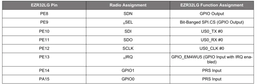
Communications between the radio and MCU are done over USART, PRS and IRQ, which requires the pins to be configured in the following way:
Table 3.1. Radio MCU Communication Configuration
EZR32LG Pin Radio Assignment EZR32LG Function Assignment
PE8 SDN GPIO Output
PE9 nSEL Bit-Banged SPI.CS (GPIO Output)
PE10 SDI US0_TX #0
PE11 SDO US0_RX #0
PE12 SCLK US0_CLK #0
PE13 nIRQ GPIO_EM4WU5 (GPIO Input with IRQ
ena-bled)
PE14 GPIO1 PRS Input
3.1.30.1 EZRadio® and EZRadioPRO® Transceivers GPIO Configuration
The EZRadio and EZRadioPRO Transceivers have four General Purpose Digital I/O pins. These GPIOs may be configured to perform various radio-specific functions, including Clock Output, FIFO Status, POR, Wake-up Timer, TRSW, AntDiversity control, etc.
Two of the radio GPIO pins are directly connected to pins on the package (GPIO2 and GPIO3). However, the remaining two radio GPIO pins (GPIO0 and GPIO1) connect internally on the EZR32LG to the pins shown in 3.1.30 EZRadio® and EZRadioPro® Transceivers.
These radio GPIOs may be routed to external package pins using the EZR32LG’s peripheral reflex system (PRS). Note that the maxi-mum frequency of the GPIO pins routed through PRS pins may be limited to ~10 MHz.
Below is some example code illustrating how to configure the EZR32LG PRS system to output the radio GPIO0/GPIO1 functions to EZR32LG pins PA0 / PA1, respectively. Note that the radio GPIO0/GPIO1 functions could also be connected to EZR32LG pins PF3/ PF4.
/* PRS routing radio GPIO0 and GPIO1 to external pin PA0&PA1 */
/ * Note that this code example uses the emlib library functions for CMU, GPIO, and PRS */ /* Enable PRS clock */
CMU_ClockEnable(cmuClock_PRS, true); /* Setup input pins */
GPIO_PinModeSet(gpioPortA, 15, gpioModeInput, 0); GPIO_PinModeSet(gpioPortE, 14, gpioModeInput, 0); /* Setup output pins */
GPIO_PinModeSet(gpioPortA, 0, gpioModePushPull, 0); GPIO_PinModeSet(gpioPortA, 1, gpioModePushPull, 0); /* Configure INT/PRS channels */
GPIO_IntConfig(gpioPortA, 15, false, false, false); GPIO_IntConfig(gpioPortE, 14, false, false, false);
/* Setup PRS */
PRS_SourceAsyncSignalSet(0, PRS_CH_CTRL_SOURCESEL_GPIOH, PRS_CH_CTRL_SIGSEL_GPIOPIN15); PRS_SourceAsyncSignalSet(1, PRS_CH_CTRL_SOURCESEL_GPIOH, PRS_CH_CTRL_SIGSEL_GPIOPIN14); PRS->ROUTE = (PRS_ROUTE_CH0PEN | PRS_ROUTE_CH1PEN);
/* Make sure PRS sensing is enabled (should be by default) */ GPIO_InputSenseSet(GPIO_INSENSE_PRS, GPIO_INSENSE_PRS);
Module Configuration Pin Connections
Cortex-M3 Full configuration NA
DBG Full configuration DBG_SWCLK, DBG_SWDIO, DBG_SWO
MSC Full configuration NA
DMA Full configuration NA
RMU Full configuration NA
EMU Full configuration NA
CMU Full configuration CMU_OUT0, CMU_OUT1
WDOG Full configuration NA
PRS Full configuration NA
USB Full configuration USB_VBUS, USB_VBUSEN, USB_VREGI,
USB_VREGO, USB_DM, USB_DMPU, USB_DP, USB_ID
I2C0 Full configuration I2C0_SDA, I2C0_SCL
I2C1 Full configuration I2C1_SDA, I2C1_SCL
USARTRF0 Full configuration with IrDA US0_TX, US0_RX, US0_CLK, US0_CS
USART1 Full configuration with I2S US1_TX, US1_RX, US1_CLK, US1_CS
USART2 Full configuration with I2S US2_TX, US2_RX, US2_CLK, US2_CS
UART0 Full configuration U0_TX, U0_RX
UART1 Full configuration U1_TX, U1_RX
LEUART0 Full configuration LEU0_TX, LEU0_RX
LEUART1 Full configuration LEU1_TX, LEU1_RX
TIMER0 Full configuration with DTI TIM0_CC[2:0], TIM0_CDTI[2:0]
TIMER1 Full configuration TIM1_CC[2:0]
TIMER2 Full configuration TIM2_CC[2:0]
TIMER3 Full configuration TIM3_CC[2:0]
RTC Full configuration NA
BURTC Full configuration NA
LETIMER0 Full configuration LET0_O[1:0]
PCNT0 Full configuration, 16-bit count register PCNT0_S[1:0]
PCNT1 Full configuration, 8-bit count register PCNT1_S[1:0]
PCNT2 Full configuration, 8-bit count register PCNT2_S[1:0]
Module Configuration Pin Connections
VCMP Full configuration NA
ADC0 Full configuration ADC0_CH[7:0]
DAC0 Full configuration DAC0_OUT[1:0]
OPAMP Full configuration Outputs: OPAMP_OUTx,
OPAMP_OUT-xALT, Inputs: OPAMP_Px, OPAMP_Nx
AES Full configuration NA
GPIO 38 pins Available pins are shown in 5.4 GPIO
Pin-out Overview
3.3 Memory Map
The EZR32LG330 memory map is shown below with RAM and flash sizes for the largest memory configuration.
The typical data are based on TAMB = 25°C and VDD = 3.0 V, as defined in Table 4.3 General Operating Conditions on page 16, by simulation and/or technology characterisation unless otherwise specified.
4.1.2 Minimum and Maximum Values
The minimum and maximum values represent the worst conditions of ambient temperature, supply voltage and frequencies, as defined in Table 4.3 General Operating Conditions on page 16, by simulation and/or technology characterisation unless otherwise specified. 4.2 Absolute Maximum Ratings
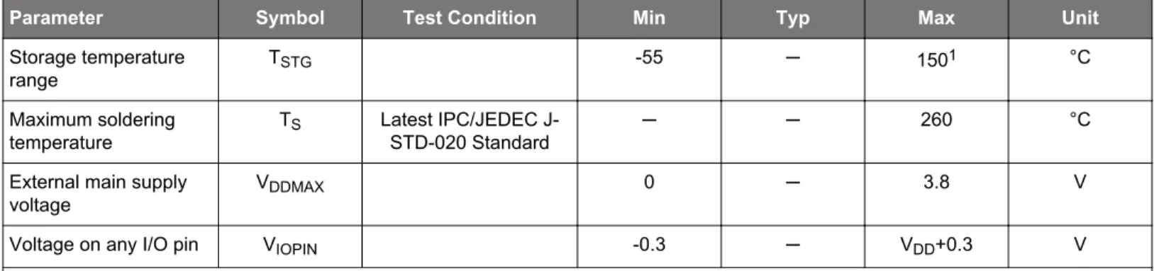
The absolute maximum ratings are stress ratings, and functional operation under such conditions are not guaranteed. Stress beyond the limits specified in the table below may affect the device reliability or cause permanent damage to the device. Functional operating conditions are given in Table 4.3 General Operating Conditions on page 16.
Table 4.1. Absolute Maximum Ratings
Parameter Symbol Test Condition Min Typ Max Unit
Storage temperature
range TSTG -55 ─ 150
1 °C
Maximum soldering
temperature TS Latest IPC/JEDEC J-STD-020 Standard ─ ─ 260 °C
External main supply
voltage VDDMAX 0 ─ 3.8 V
Voltage on any I/O pin VIOPIN -0.3 ─ VDD+0.3 V
Note:
1. Based on programmed devices tested for 10000 hours at 150 ºC. Storage temperature affects retention of preprogrammed cali-bration values stored in flash. Refer to the Flash section in the Electrical Characteristics for information on flash data retention for different temperatures.
4.3 Thermal Characteristics
Table 4.2. Thermal Conditions
Parameter Symbol Test Condition Min Typ Max Unit
Ambient temperature range TAMB -40 ─ 85 °C
Junction temperature value TJ ─ ─ 1051 °C
Thermal impedance junction
to ambient TIJA
+13/+16 dBm on
2-layer board ─ ─ 61.8 °C/W
+20 dBm on 4-layer
board ─ ─ 20.72 °C/W
Storage temperature range TSTG -55 ─ 150 °C
Note:
1. Values are based on simulations run on 2-layer and 4-layer PCBs at 0m/s airflow.
2. Based on programmed devices tested for 10000 hours at 150 ºC. Storage temperature affects retention of preprogrammed cali-bration values stored in flash. Refer to the Flash section in the Electrical Characteristics for information on flash data retention for different temperatures.
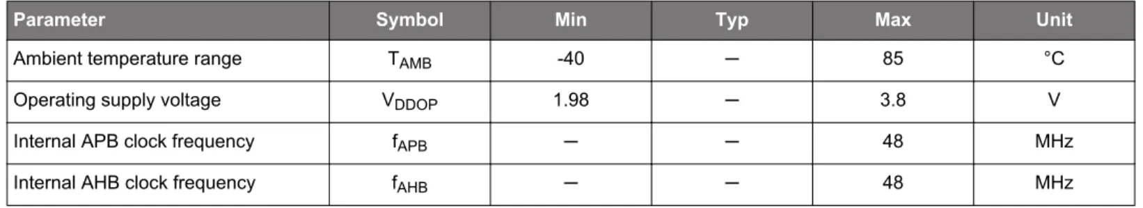
4.4 General Operating Conditions
Table 4.3. General Operating Conditions
Parameter Symbol Min Typ Max Unit
Ambient temperature range TAMB -40 ─ 85 °C
Operating supply voltage VDDOP 1.98 ─ 3.8 V
Internal APB clock frequency fAPB ─ ─ 48 MHz
EM0 current. No prescal-ing. Running prime num-ber calculation code from Flash. (Production test condition = 14 MHz)
IEM0
48 MHz HFXO, all peripheral clocks disabled, VDD= 3.0 V, TAMB=25 °C
─ 211 225 µA/MHz
48 MHz HFXO, all peripheral clocks disabled, VDD= 3.0 V, TAMB=85 °C
─ 211 230 µA/MHz
28 MHz HFRCO, all peripheral clocks disabled, VDD= 3.0 V, TAMB=25 °C
─ 212 220 µA/MHz
28 MHz HFRCO, all peripheral clocks
disabled, VDD= 3.0 V, TAMB=85 °C ─ 213 223 µA/MHz
21 MHz HFRCO, all peripheral clocks
disabled, VDD= 3.0 V, TAMB=25 °C ─ 214 224 µA/MHz
21 MHz HFRCO, all peripheral clocks
disabled, VDD= 3.0 V, TAMB=85 °C ─ 215 226 µA/MHz
14 MHz HFRCO, all peripheral clocks disabled, VDD= 3.0 V, TAMB=25 °C
─ 216 231 µA/MHz
14 MHz HFRCO, all peripheral clocks disabled, VDD= 3.0 V, TAMB=85 °C
─ 217 237 µA/MHz
11 MHz HFRCO, all peripheral clocks disabled, VDD= 3.0 V, TAMB=25 °C
─ 218 239 µA/MHz
11 MHz HFRCO, all peripheral clocks
disabled, VDD= 3.0 V, TAMB=85 °C ─ 219 239 µA/MHz
6.6 MHz HFRCO, all peripheral clocks
disabled, VDD= 3.0 V, TAMB=25 °C ─ 224 242 µA/MHz
6.6 MHz HFRCO, all peripheral clocks
disabled, VDD= 3.0 V, TAMB=85 °C ─ 224 250 µA/MHz
1.2 MHz HFRCO, all peripheral clocks disabled, VDD= 3.0 V, TAMB=25 °C
─ 257 285 µA/MHz
1.2 MHz HFRCO, all peripheral clocks disabled, VDD= 3.0 V, TAMB=85 °C
Parameter Symbol Test Condition Min Typ Max Unit
EM1 current (Production
test condition = 14 MHz) IEM1
48 MHz HFXO, all peripheral clocks disabled, VDD= 3.0 V, TAMB=25 °C
─ 63 75 µA/MHz
48 MHz HFXO, all peripheral clocks disabled, VDD= 3.0 V, TAMB=85 °C
─ 65 76 µA/MHz
28 MHz HFRCO, all peripheral clocks
disabled, VDD= 3.0 V, TAMB=25 °C ─ 64 75 µA/MHz
28 MHz HFRCO, all peripheral clocks
disabled, VDD= 3.0 V, TAMB=85 °C ─ 65 77 µA/MHz
21 MHz HFRCO, all peripheral clocks
disabled, VDD= 3.0 V, TAMB=25 °C ─ 65 76 µA/MHz
21 MHz HFRCO, all peripheral clocks disabled, VDD= 3.0 V, TAMB=85 °C
─ 66 78 µA/MHz
14 MHz HFRCO, all peripheral clocks disabled, VDD= 3.0 V, TAMB=25 °C
─ 67 79 µA/MHz
14 MHz HFRCO, all peripheral clocks disabled, VDD= 3.0 V, TAMB=85 °C
─ 68 82 µA/MHz
11 MHz HFRCO, all peripheral clocks
disabled, VDD= 3.0 V, TAMB=25 °C ─ 68 81 µA/MHz
11 MHz HFRCO, all peripheral clocks
disabled, VDD= 3.0 V, TAMB=85 °C ─ 70 83 µA/MHz
6.6 MHz HFRCO, all peripheral clocks
disabled, VDD= 3.0 V, TAMB=25 °C ─ 74 87 µA/MHz
6.6 MHz HFRCO, all peripheral clocks disabled, VDD= 3.0 V, TAMB=85 °C
─ 76 89 µA/MHz
1.2 MHz HFRCO. all peripheral clocks disabled, VDD= 3.0 V, TAMB=25 °C
─ 106 120 µA/MHz
1.2 MHz HFRCO. all peripheral clocks disabled, VDD= 3.0 V, TAMB=85 °C
─ 112 129 µA/MHz
EM2 current IEM2
EM2 current with RTC prescaled to 1 Hz, 32.768 kHz LFRCO, VDD= 3.0 V,
TAMB=25 °C
─ 0.951 1.7 µA
EM2 current with RTC prescaled to 1 Hz, 32.768 kHz LFRCO, VDD= 3.0 V,
TAMB=85 °C
─ 3.01 4.01 µA
EM3 current IEM3
VDD= 3.0 V, TAMB=25 °C ─ 0.65 1.3 µA
VDD= 3.0 V, TAMB=85 °C ─ 2.65 4.0 µA
EM4 current IEM4 VDD= 3.0 V, TAMB=25 °C ─ 0.02 0.055 µA
VDD= 3.0 V, TAMB=85 °C ─ 0.44 0.9 µA
Note:
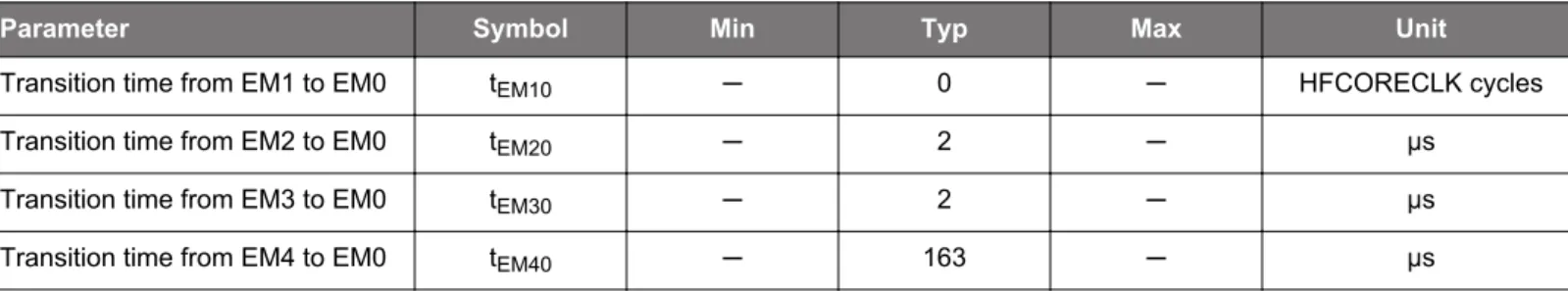
Parameter Symbol Min Typ Max Unit
Transition time from EM1 to EM0 tEM10 ─ 0 ─ HFCORECLK cycles
Transition time from EM2 to EM0 tEM20 ─ 2 ─ µs
Transition time from EM3 to EM0 tEM30 ─ 2 ─ µs
Transition time from EM4 to EM0 tEM40 ─ 163 ─ µs
4.7 Power Management
The EZR32LG requires the AVDD_x, VDD_DREG and IOVDD_x pins to be connected together (with optional filter) at the PCB level. For practical schematic recommendations, see the application note, AN0002.0: EFM32 and EZR32 Wireless MCU Series 0 Hardware Design Considerations.
Table 4.6. Power Management
Parameter Symbol Test Condition Min Typ Max Unit
BOD threshold on falling external
supply voltage VBODextthr- 1.74 ─ 1.96 V
BOD threshold on falling internally
regulated supply voltage VBODintthr- 1.57 ─ 1.7 V
BOD threshold on rising external
supply voltage VBODextthr+ ─ 1.85 1.98 V
Power-on Reset (POR) threshold
on rising external supply voltage VPORthr+ ─ ─ 1.98 V
Delay from reset is released until
program execution starts tRESET set, Brown-out Reset andApplies to Power-on Re-pin reset.
─ 163 ─ µs
Voltage regulator decoupling
ca-pacitor. CDECOUPLE X5R capacitor recommen-ded. Apply between DE-COUPLE pin and
GROUND
4.8 Flash
Table 4.7. Flash
Parameter Symbol Test Condition Min Typ Max Unit
Flash erase cycles before failure ECFLASH 20000 ─ ─ cycles
Flash data retention RETFLASH
TAMB<150 °C 10000 ─ ─ h
TAMB<85 °C 10 ─ ─ years
TAMB<70 °C 20 ─ ─ years
Word (32-bit) programming time tW_PROG 20 ─ ─ µs
Page erase time tPERASE 20 20.4 20.8 ms
Device erase time tDERASE 40 40.8 41.6 ms
Erase current IERASE ─ ─ 71 mA
Write current IWRITE ─ ─ 71 mA
Supply voltage during flash erase
and write VFLASH 1.98 ─ 3.8 V
Note:
Input low voltage VIOIL ─ ─ 0.30 VDD V
Input high voltage VIOIH 0.70 VDD ─ ─ V
Output high voltage (Production test condition = 3.0 V,
DRIVE-MODE = STANDARD) VIOOH
Sourcing 0.1 mA, VDD = 1.98 V, GPIO_Px_CTRL DRIVEMODE = LOWEST ─ 0.80 VDD ─ V Sourcing 0.1 mA, VDD = 3.0 V, GPIO_Px_CTRL DRIVEMODE = LOWEST ─ 0.90 VDD ─ V Sourcing 1 mA, VDD = 1.98 V, GPIO_Px_CTRL DRIVEMODE = LOW ─ 0.85 VDD ─ V Sourcing 1 mA, VDD = 3.0 V, GPIO_Px_CTRL DRIVEMODE = LOW ─ 0.90 VDD ─ V Sourcing 6 mA, VDD = 1.98 V, GPIO_Px_CTRL DRIVEMODE = STANDARD 0.75 VDD ─ ─ V Sourcing 6 mA, VDD = 3.0 V, GPIO_Px_CTRL DRIVEMODE = STANDARD 0.85 VDD ─ ─ V Sourcing 20 mA, VDD = 1.98 V, GPIO_Px_CTRL DRIVEMODE = HIGH 0.60 VDD ─ ─ V Sourcing 20 mA, VDD = 3.0 V, GPIO_Px_CTRL DRIVEMODE = HIGH 0.80 VDD ─ ─ V
Parameter Symbol Test Condition Min Typ Max Unit
Output low voltage (Production test condition = 3.0 V, DRIVE-MODE = STANDARD)
VIOOL Sinking 0.1 mA, VDD = 1.98 V, GPIO_Px_CTRL DRIVEMODE = LOWEST ─ 0.20 VDD ─ V Sinking 0.1 mA, VDD = 3.0 V, GPIO_Px_CTRL DRIVEMODE = LOWEST ─ 0.10 VDD ─ V Sinking 1 mA, VDD = 1.98 V, GPIO_Px_CTRL DRIVEMODE = LOW ─ 0.10 VDD ─ V Sinking 1 mA, VDD = 3.0 V, GPIO_Px_CTRL DRIVEMODE = LOW ─ 0.05 VDD V Sinking 6 mA, VDD = 1.98 V, GPIO_Px_CTRL DRIVEMODE = STANDARD ─ ─ 0.30 VDD V Sinking 6 mA, VDD = 3.0 V, GPIO_Px_CTRL DRIVEMODE = STANDARD ─ ─ 0.20 VDD V Sinking 20 mA, VDD = 1.98 V, GPIO_Px_CTRL DRIVEMODE = HIGH ─ ─ 0.35 VDD V Sinking 20 mA, VDD = 3.0 V, GPIO_Px_CTRL DRIVEMODE = HIGH ─ ─ 0.25 VDD V
Input leakage current IIOLEAK High Impedance IO connected
to GROUND or Vdd ─ ±0.1 ±40 nA
I/O pin pull-up resistor RPU ─ 40 ─ kΩ
I/O pin pull-down resistor RPD ─ 40 ─ kΩ
Internal ESD series resistor RIOESD ─ 200 ─ Ω
Pulse width of pulses to be re-moved by the glitch suppression filter
tIOGLITCH 10 ─ 50 ns
Output fall time
tIOOF GPIO_Px_CTRL DRIVEMODE = LOWEST and load capaci-tance CL = 12.5-25 pF.
20+0.1 CL ─ 250 ns
GPIO_Px_CTRL DRIVEMODE = LOW and load capacitance CL = 350-600 pF
20+0.1 CL ─ 250 ns
I/O pin hysteresis (VIOTHR+
0.0 0.5 1.0 1.5 2.0 Low-Level Output Voltage [V]
0.00 0.05 0.10 0.15 Lo w-Le
vel Output Current [mA]
-40°C 25°C 85°C
GPIO_Px_CTRL DRIVEMODE = LOWEST
0.0 0.5 1.0 1.5 2.0
Low-Level Output Voltage [V] 0 1 2 3 4 Lo w-Le
vel Output Current [mA]
-40°C 25°C 85°C
GPIO_Px_CTRL DRIVEMODE = LOW
0.0 0.5 1.0 1.5 2.0
Low-Level Output Voltage [V] 0 5 10 15 20 Lo w-Le
vel Output Current [mA]
-40°C 25°C 85°C
GPIO_Px_CTRL DRIVEMODE = STANDARD
0.0 0.5 1.0 1.5 2.0
Low-Level Output Voltage [V] 0 5 10 15 20 25 30 35 40 45 Lo w-Le
vel Output Current [mA]
-40°C 25°C 85°C
GPIO_Px_CTRL DRIVEMODE = High Figure 4.1. Typical Low-Level Output Current, 2 V Supply Voltage
0.0 0.5 1.0 1.5 2.0 High-Level Output Voltage [V]
–0.20 –0.15 –0.10 –0.05 0.00 High-Le
vel Output Current [mA]
-40°C 25°C 85°C
GPIO_Px_CTRL DRIVEMODE = LOWEST
0.0 0.5 1.0 1.5 2.0
High-Level Output Voltage [V] –2.5 –2.0 –1.5 –1.0 –0.5 0.0 High-Le
vel Output Current [mA]
-40°C 25°C 85°C
GPIO_Px_CTRL DRIVEMODE = LOW
0.0 0.5 1.0 1.5 2.0
High-Level Output Voltage [V] –20 –15 –10 –5 0 High-Le
vel Output Current [mA]
-40°C 25°C 85°C
GPIO_Px_CTRL DRIVEMODE = STANDARD
0.0 0.5 1.0 1.5 2.0
High-Level Output Voltage [V] –50 –40 –30 –20 –10 0 High-Le
vel Output Current [mA]
-40°C 25°C 85°C
GPIO_Px_CTRL DRIVEMODE = High Figure 4.2. Typical High-Level Output Current, 2 V Supply Voltage
0.0 0.5 1.0 1.5 2.0 2.5 3.0 Low-Level Output Voltage [V]
0.0 0.1 0.2 0.3 0.4 Lo w-Le
vel Output Current [mA]
-40°C 25°C 85°C
GPIO_Px_CTRL DRIVEMODE = LOWEST
0.0 0.5 1.0 1.5 2.0 2.5 3.0
Low-Level Output Voltage [V] 0 2 4 6 8 Lo w-Le
vel Output Current [mA]
-40°C 25°C 85°C
GPIO_Px_CTRL DRIVEMODE = LOW
0.0 0.5 1.0 1.5 2.0 2.5 3.0
Low-Level Output Voltage [V] 0 5 10 15 20 25 30 35 40 Lo w-Le
vel Output Current [mA]
-40°C 25°C 85°C
GPIO_Px_CTRL DRIVEMODE = STANDARD
0.0 0.5 1.0 1.5 2.0 2.5 3.0
Low-Level Output Voltage [V] 0 10 20 30 40 50 Lo w-Le
vel Output Current [mA]
-40°C 25°C 85°C
GPIO_Px_CTRL DRIVEMODE = High Figure 4.3. Typical Low-Level Output Current, 3 V Supply Voltage
0.0 0.5 1.0 1.5 2.0 2.5 3.0 High-Level Output Voltage [V]
–0.5 –0.4 –0.3 –0.2 –0.1 0.0 High-Le
vel Output Current [mA]
-40°C 25°C 85°C
GPIO_Px_CTRL DRIVEMODE = LOWEST
0.0 0.5 1.0 1.5 2.0 2.5 3.0
High-Level Output Voltage [V] –6 –5 –4 –3 –2 –1 0 High-Le
vel Output Current [mA]
-40°C 25°C 85°C
GPIO_Px_CTRL DRIVEMODE = LOW
0.0 0.5 1.0 1.5 2.0 2.5 3.0
High-Level Output Voltage [V] –50 –40 –30 –20 –10 0 High-Le
vel Output Current [mA]
-40°C 25°C 85°C
GPIO_Px_CTRL DRIVEMODE = STANDARD
0.0 0.5 1.0 1.5 2.0 2.5 3.0
High-Level Output Voltage [V] –50 –40 –30 –20 –10 0 High-Le
vel Output Current [mA]
-40°C 25°C 85°C
GPIO_Px_CTRL DRIVEMODE = High Figure 4.4. Typical High-Level Output Current, 3 V Supply Voltage
0.0 0.5 1.0 1.5 2.0 2.5 3.0 3.5 Low-Level Output Voltage [V]
0.0 0.1 0.2 0.3 0.4 0.5 0.6 Lo w-Le
vel Output Current [mA]
-40°C 25°C 85°C
GPIO_Px_CTRL DRIVEMODE = LOWEST
0.0 0.5 1.0 1.5 2.0 2.5 3.0 3.5
Low-Level Output Voltage [V] 0 2 4 6 8 10 Lo w-Le
vel Output Current [mA]
-40°C 25°C 85°C
GPIO_Px_CTRL DRIVEMODE = LOW
0.0 0.5 1.0 1.5 2.0 2.5 3.0 3.5
Low-Level Output Voltage [V] 0 10 20 30 40 50 Lo w-Le
vel Output Current [mA]
-40°C 25°C 85°C
GPIO_Px_CTRL DRIVEMODE = STANDARD
0.0 0.5 1.0 1.5 2.0 2.5 3.0 3.5
Low-Level Output Voltage [V] 0 10 20 30 40 50 Lo w-Le
vel Output Current [mA]
-40°C 25°C 85°C
GPIO_Px_CTRL DRIVEMODE = High Figure 4.5. Typical Low-Level Output Current, 3.8 V Supply Voltage
0.0 0.5 1.0 1.5 2.0 2.5 3.0 3.5 High-Level Output Voltage [V]
–0.8 –0.7 –0.6 –0.5 –0.4 –0.3 –0.2 –0.1 0.0 High-Le
vel Output Current [mA]
-40°C 25°C 85°C
GPIO_Px_CTRL DRIVEMODE = LOWEST
0.0 0.5 1.0 1.5 2.0 2.5 3.0 3.5
High-Level Output Voltage [V] –9 –8 –7 –6 –5 –4 –3 –2 –1 0 High-Le
vel Output Current [mA]
-40°C 25°C 85°C
GPIO_Px_CTRL DRIVEMODE = LOW
0.0 0.5 1.0 1.5 2.0 2.5 3.0 3.5
High-Level Output Voltage [V] –50 –40 –30 –20 –10 0 High-Le
vel Output Current [mA]
-40°C 25°C 85°C
GPIO_Px_CTRL DRIVEMODE = STANDARD
0.0 0.5 1.0 1.5 2.0 2.5 3.0 3.5
High-Level Output Voltage [V] –50 –40 –30 –20 –10 0 High-Le
vel Output Current [mA]
-40°C 25°C 85°C
GPIO_Px_CTRL DRIVEMODE = High Figure 4.6. Typical High-Level Output Current, 3.8 V Supply Voltage
Parameter Symbol Test Condition Min Typ Max Unit
Supported nominal crystal
fre-quency fLFXO 31.3 32.768 34.3 kHz
Supported crystal equivalent
series resistance (ESR) ESRLFXO ─ 30 120 kΩ
Supported crystal external load
range CLFXOL X
1 ─ 25 pF
Duty cycle DCLFXO 48 50 53.5 %
Current consumption for core
and buffer after startup ILFXO ESR=30 kΩ, CBOOST in CMU_CTRL is 1L=10 pF, LFXO- ─ 190 ─ nA
Start- up time tLFXO ESR=30 kΩ, CL=10 pF, 40%
-60% duty cycle has been reached, LFXOBOOST in
CMU_CTRL is 1
─ 1100 ─ ms
Note:
1. See Minimum Load Capacitance (CLFXOL) Requirement For Safe Crystal Startup in energyAware Designer in Simplicity Studio. For safe startup of a given crystal, the Configurator tool in Simplicity Studio contains a tool to help users configure both load capaci-tance and software settings for using the LFXO. For details regarding the crystal configuration, refer to application note, AN0016.0: EFM32 Oscillator Design Considerations.
4.10.2 HFXO
Table 4.10. HFXO
Parameter Symbol Test Condition Min Typ Max Unit
Supported nominal crystal
Frequency fHFXO 4 ─ 48 MHz
Supported crystal equivalent
series resistance (ESR) ESRHFXO
Crystal frequency 48 MHz ─ ─ 50 Ω
Crystal frequency 32 MHz ─ 30 60 Ω
Crystal frequency 4 MHz ─ 400 1500 Ω
The transconductance of the HFXO input transistor at crys-tal startup
gmHFXO HFXOBOOST in CMU_CTRL equals
0b11 20 ─ ─ ms
Supported crystal external
load range CHFXOL 5 ─ 25 pF
Duty cycle DCHFXO 46 50 54 %
Current consumption for
HFXO after startup IHFXO
4 MHz: ESR=400 Ohm, CL=20 pF, HFXOBOOST in CMU_CTRL equals
0b11
─ 85 ─ µA
32 MHz: ESR=30 Ohm, CL=10 pF, HFXOBOOST in CMU_CTRL equals
0b11
─ 165 ─ µA
Startup time tHFXO 32 MHz: ESR=30 Ohm, CL=10 pF,
HFXOBOOST in CMU_CTRL equals 0b11
Oscillation frequency , VDD= 3.0 V, TAMB=25 °C
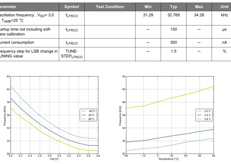
fLFRCO 31.29 32.768 34.28 kHz
Startup time not including
soft-ware calibration tLFRCO ─ 150 ─ µs
Current consumption ILFRCO ─ 300 ─ nA
Frequency step for LSB change in
TUNING value STEPTUNE-LFRCO ─ 1.5 ─ %
2.0 2.2 2.4 2.6 2.8 3.0 3.2 3.4 3.6 3.8 Vdd [V] 30 32 34 36 38 40 42 Frequency [kHz] -40°C 25°C 85°C –40 –15 5 25 45 65 85 Temperature [°C] 30 32 34 36 38 40 42 Frequency [kHz] 2.0 V 3.0 V 3.8 V
4.10.4 HFRCO
Table 4.12. HFRCO
Parameter Symbol Test Condition Min Typ Max Unit
Oscillation frequency, VDD= 3.0 V, TAMB=25 °C fHFRCO 28 MHz frequency band 27.5 28.0 28.5 MHz 21 MHz frequency band 20.6 21.0 21.4 MHz 14 MHz frequency band 13.7 14.0 14.3 MHz 11 MHz frequency band 10.8 11.0 11.2 MHz 7 MHz frequency band 6.48 6.60 6.72 MHz 1 MHz frequency band 1.15 1.20 1.25 MHz
Settling time after start-up t HFRCO_set-tling
fHFRCO = 14 MHz ─ 0.6 ─ Cycles
Current consumption IHFRCO
fHFRCO = 28 MHz ─ 165 215 µA fHFRCO = 21 MHz ─ 134 175 µA fHFRCO = 14 MHz ─ 106 140 µA fHFRCO = 11 MHz ─ 94 125 µA fHFRCO = 6.6 MHz ─ 77 105 µA fHFRCO = 1.2 MHz ─ 25 40 µA
Duty cycle DCHFRCO fHFRCO = 14 MHz 48.5 50 51 %
Frequency step for LSB
change in TUNING value STEPTUNE-HFRC O
─ 0.31 ─ %
Note:
1. The TUNING field in the CMU_HFRCOCTRL register may be used to adjust the HFRCO frequency. There is enough adjustment range to ensure that the frequency bands above 7 MHz will always have some overlap across supply voltage and temperature. By using a stable frequency reference such as the LFXO or HFXO, a firmware calibration routine can vary the TUNING bits and the frequency band to maintain the HFRCO frequency at any arbitrary value between 7 MHz and 28 MHz across operating condi-tions.
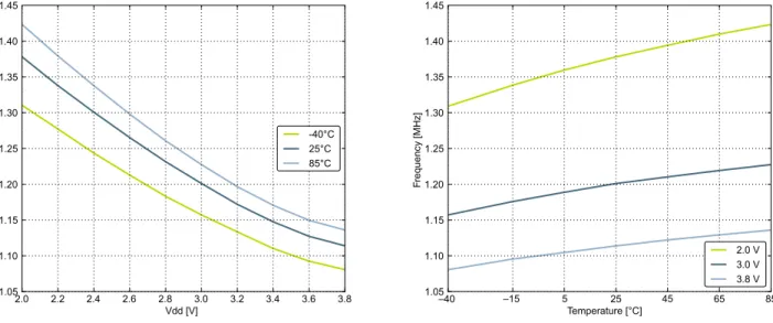
2.0 2.2 2.4 2.6 2.8 3.0 3.2 3.4 3.6 3.8 Vdd [V] 1.05 1.10 1.15 1.20 1.25 1.30 Frequency [MHz] -40°C 25°C 85°C –40 –15 5 25 45 65 85 Temperature [°C] 1.05 1.10 1.15 1.20 1.25 1.30 Frequency [MHz] 2.0 V 3.0 V 3.8 V
Figure 4.8. Calibrated HFRCO 1 MHz Band Frequency vs Supply Voltage and Temperature
2.0 2.2 2.4 2.6 2.8 3.0 3.2 3.4 3.6 3.8 Vdd [V] 6.30 6.35 6.40 6.45 6.50 6.55 6.60 6.65 6.70 Frequency [MHz] -40°C 25°C 85°C –40 –15 5 25 45 65 85 Temperature [°C] 6.30 6.35 6.40 6.45 6.50 6.55 6.60 6.65 6.70 Frequency [MHz] 2.0 V 3.0 V 3.8 V
2.0 2.2 2.4 2.6 2.8 3.0 3.2 3.4 3.6 3.8 Vdd [V] 10.6 10.7 10.8 10.9 11.0 11.1 11.2 Frequency [MHz] -40°C 25°C 85°C –40 –15 5 25 45 65 85 Temperature [°C] 10.6 10.7 10.8 10.9 11.0 11.1 11.2 Frequency [MHz] 2.0 V 3.0 V 3.8 V
Figure 4.10. Calibrated HFRCO 11 MHz Band Frequency vs Supply Voltage and Temperature
2.0 2.2 2.4 2.6 2.8 3.0 3.2 3.4 3.6 3.8 Vdd [V] 13.4 13.5 13.6 13.7 13.8 13.9 14.0 14.1 14.2 Frequency [MHz] -40°C 25°C 85°C –40 –15 5 25 45 65 85 Temperature [°C] 13.4 13.5 13.6 13.7 13.8 13.9 14.0 14.1 14.2 Frequency [MHz] 2.0 V 3.0 V 3.8 V
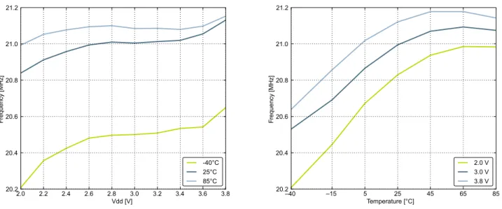
2.0 2.2 2.4 2.6 2.8 3.0 3.2 3.4 3.6 3.8 Vdd [V] 20.2 20.4 20.6 20.8 Frequency [MHz] -40°C 25°C 85°C –40 –15 5 25 45 65 85 Temperature [°C] 20.2 20.4 20.6 20.8 Frequency [MHz] 2.0 V 3.0 V 3.8 V
Figure 4.12. Calibrated HFRCO 21 MHz Band Frequency vs Supply Voltage and Temperature
2.0 2.2 2.4 2.6 2.8 3.0 3.2 3.4 3.6 3.8 Vdd [V] 26.8 27.0 27.2 27.4 27.6 27.8 28.0 28.2 Frequency [MHz] -40°C 25°C 85°C –40 –15 5 25 45 65 85 Temperature [°C] 26.8 27.0 27.2 27.4 27.6 27.8 28.0 28.2 28.4 Frequency [MHz] 2.0 V 3.0 V 3.8 V
4.10.5 AUXHFRCO
Table 4.13. AUXHFRCO
Parameter Symbol Test Condition Min Typ Max Unit
Oscillation frequency, VDD= 3.0 V, TAMB=25 °C fAUXHFRCO 28 MHz frequency band 27.5 28.0 28.5 MHz 21 MHz frequency band 20.6 21.0 21.4 MHz 14 MHz frequency band 13.7 14.0 14.3 MHz 11 MHz frequency band 10.8 11.0 11.2 MHz 7 MHz frequency band 6.481 6.601 6.721 MHz 1 MHz frequency band 1.152 1.202 1.252 MHz
Settling time after start-up t AUXHFR-CO_settling
fAUXHFRCO = 14 MHz ─ 0.6 ─ Cycles
Frequency step for LSB
change in TUNING value STEPTUNE-AUXHFR CO
─ 0.33 ─ %
Note:
1. For devices with prod. rev. < 19, Typ = 7 MHz and Min/Max values not applicable. 2. For devices with prod. rev. < 19, Typ = 1 MHz and Min/Max values not applicable.
3. The TUNING field in the CMU_AUXHFRCOCTRL register may be used to adjust the AUXHFRCO frequency. There is enough adjustment range to ensure that the frequency bands above 7 MHz will always have some overlap across supply voltage and temperature. By using a stable frequency reference such as the LFXO or HFXO, a firmware calibration routine can vary the TUN-ING bits and the frequency band to maintain the AUXHFRCO frequency at any arbitrary value between 7 MHz and 28 MHz across operating conditions.
4.10.6 ULFRCO
Table 4.14. ULFRCO
Parameter Symbol Test Condition Min Typ Max Unit
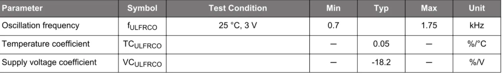
Oscillation frequency fULFRCO 25 °C, 3 V 0.7 1.75 kHz
Temperature coefficient TCULFRCO ─ 0.05 ─ %/°C
Input voltage range VADCIN Single-ended 0 — VREF V
Differential -VREF/2 — VREF/2 V
Input range of external refer-ence voltage, single-ended and differential
VADCREFIN 1.25 — VDD V
Input range of external nega-tive reference voltage on channel 7
VADCREFIN_CH7 See VADCREFIN 0 — VDD - 1.1 V
Input range of external posi-tive reference voltage on channel 6
VADCREFIN_CH6 See VADCREFIN 0.625 — VDD V
Common mode input range VADCCMIN 0 — VDD V
Input current IADCIN 2 pF sampling capacitors — <100 — nA
Analog input common mode
rejection ratio CMRRADC — 65 — dB
Average active current IADC 1 MSamples/s, 12-bit, external
reference — 351
1 — µA
10 kSamples/s 12-bit, internal 1.25 V reference, WARMUP-MODE in ADCn_CTRL set to
0b00
— 67 1 — µA
10 kSamples/s 12-bit, internal 1.25 V reference, WARMUP-MODE in ADCn_CTRL set to
0b01
— 63 1 — µA
10 kSamples/s 12-bit, internal 1.25 V reference, WARMUP-MODE in ADCn_CTRL set to
0b10
— 64 1 — µA
Input capacitance CADCIN — 2 — pF
Input ON resistance RADCIN 300 — 800 Ω
Input RC filter resistance RADCFILT — 10 — kΩ
Input RC filter/decoupling
ca-pacitance CADCFILT — 250 — fF
Input bias current IADCBIASIN VSS < VIN < VDD -40 — 40 nA
Input offset current IADCOFFSETIN VSS < VIN < VDD -40 — 40 nA
Parameter Symbol Test Condition Min Typ Max Unit
Conversion time tADCCONV 6-bit 7 — — ADCCLK
Cycles
8-bit 11 — — ADCCLK
Cycles
12-bit 13 — — ADCCLK
Cycles
Acquisition time tADCACQ Programmable 1 — 256 ADCCLK
Cycles Required acquisition time for
VDD/3 reference tADCACQVDD3 2 — — µs
Startup time of reference
generator and ADC core tADCSTART NORMAL mode — 5 — µs
KEEPADCWARM mode — 1 — µs
Signal-to-Noise Ratio (SNR) SNRADC 1 MSamples/s, 12-bit,
single-ended, internal 1.25 V reference — 59 — dB
1 MSamples/s, 12-bit,
single-ended, internal 2.5 V reference — 63 — dB
1 MSamples/s, 12-bit,
single-ended, VDD reference — 65 — dB
1 MSamples/s, 12-bit,
differen-tial, internal 1.25 V reference — 60 — dB
1 MSamples/s, 12-bit,
differen-tial, internal 2.5 V reference — 65 — dB
1 MSamples/s, 12-bit,
differen-tial, 5 V reference — 54 — dB
1 MSamples/s, 12-bit,
differen-tial, VDD reference — 67 — dB
1 MSamples/s, 12-bit,
differen-tial, 2xVDD reference — 69 — dB
200 kSamples/s, 12-bit,
single-ended, internal 1.25 V reference — 62 — dB
200 kSamples/s, 12-bit,
single-ended, internal 2.5 V reference — 63 — dB
200 kSamples/s, 12-bit,
single-ended, VDD reference — 67 — dB
200 kSamples/s, 12-bit,
differen-tial, internal 1.25 V reference — 63 — dB
200 kSamples/s, 12-bit,
differen-tial, internal 2.5 V reference — 66 — dB
200 kSamples/s, 12-bit,
differen-tial, 5 V reference — 66 — dB
200 kSamples/s, 12-bit,
differen-tial, VDD reference 63 66 — dB
200 kSamples/s, 12-bit,
1 MSamples/s, 12-bit,
single-ended, VDD reference — 64 — dB
1 MSamples/s, 12-bit,
differen-tial, internal 1.25 V reference — 60 — dB
1 MSamples/s, 12-bit,
differen-tial, internal 2.5 V reference — 64 — dB
1 MSamples/s, 12-bit,
differen-tial, 5 V reference — 54 — dB
1 MSamples/s, 12-bit,
differen-tial, VDD reference — 66 — dB
1 MSamples/s, 12-bit,
differen-tial, 2xVDD reference — 68 — dB
200 kSamples/s, 12-bit,
single-ended, internal 1.25 V reference — 61 — dB
200 kSamples/s, 12-bit,
single-ended, internal 2.5 V reference — 65 — dB
200 kSamples/s, 12-bit,
single-ended, VDD reference — 66 — dB
200 kSamples/s, 12-bit,
differen-tial, internal 1.25 V reference — 63 — dB
200 kSamples/s, 12-bit,
differen-tial, internal 2.5 V reference — 66 — dB
200 kSamples/s, 12-bit,
differen-tial, 5V reference — 66 — dB
200 kSamples/s, 12-bit,
differen-tial, VDD reference 62 66 — dB
200 kSamples/s, 12-bit,
Parameter Symbol Test Condition Min Typ Max Unit
Spurious-Free Dynamic
Range (SFDR) SFDRADC ended, internal 1.25 V reference1 MSamples/s, 12-bit, single- — 64 — dBc 1 MSamples/s, 12-bit,
single-ended, internal 2.5 V reference — 76 — dBc
1 MSamples/s, 12-bit,
single-ended, VDD reference — 73 — dBc
1 MSamples/s, 12-bit,
differen-tial, internal 1.25 V reference — 66 — dBc
1 MSamples/s, 12-bit,
differen-tial, internal 2.5 V reference — 77 — dBc
1 MSamples/s, 12-bit,
differen-tial, VDD reference — 76 — dBc
1 MSamples/s, 12-bit,
differen-tial, 2xVDD reference — 75 — dBc
1 MSamples/s, 12-bit,
differen-tial, 5 V reference — 69 — dBc
200 kSamples/s, 12-bit,
single-ended, internal 1.25 V reference — 75 — dBc
200 kSamples/s, 12-bit,
single-ended, internal 2.5 V reference — 75 — dBc
200 kSamples/s, 12-bit,
single-ended, VDD reference — 76 — dBc
200 kSamples/s, 12-bit,
differen-tial, internal 1.25 V reference — 79 — dBc
200 kSamples/s, 12-bit,
differen-tial, internal 2.5 V reference — 79 — dBc
200 kSamples/s, 12-bit,
differen-tial, 5 V reference — 78 — dBc
200 kSamples/s, 12-bit,
differen-tial, VDD reference 68 79 — dBc
200 kSamples/s, 12-bit,
differen-tial, 2xVDD reference — 79 — dBc
Offset voltage VADCOFFSET After calibration, single-ended -3.5 0.3 3 mV
After calibration, differential — 0.3 — mV
Thermometer output gradient TGRADADCTH — -1.92 — mV/°C
— -6.3 — ADC
Co-des/°C Differential non-linearity
(DNL) DNLADC VDD= 3.0 V, external 2.5 V refer-ence
-1 ±0.7 4 LSB
Integral non-linearity (INL),
End point method INLADC VDD= 3.0 V, external 2.5 V refer-ence — ±1.2 ±3 LSB
Missing codes MCADC 11.999 2 12 — bits
2.5 V reference 2.4 2.5 2.6 V
VREF voltage drift VREF_VDRIFT 1.25 V reference -12.4 2.9 18.2 mV/V
2.5 V reference, VDD > 2.5 V -24.6 5.7 35.2 mV/V
VREF temperature drift VREF_TDRIFT 1.25 V reference -132 272 677 µV/°C
2.5 V reference -231 545 1271 µV/°C
VREF current consumption IVREF 1.25 V reference — 67 97 µA
2.5 V reference — 55 72 µA
ADC and DAC VREF
match-ing VREF_MATCH 1.25 V reference — 99.85 — %
2.5 V reference — 100.01 — %
Note:
1. Includes required contribution from the voltage reference.
2. On the average every ADC will have one missing code, most likely to appear around 2048 +/- n*512 where n can be a value in the set {-3, -2, -1, 1, 2, 3}. There will be no missing code around 2048, and in spite of the missing code the ADC will be monotonic at all times so that a response to a slowly increasing input will always be a slowly increasing output. Around the one code that is missing, the neighbor codes will look wider in the DNL plot. The spectra will show spurs on the level of -78dBc for a full-scale input for chips that have the missing code issue.
3. Typical numbers given by abs(Mean) / (85 - 25).
4. Max number given by (abs(Mean) + 3x stddev) / (85 - 25).
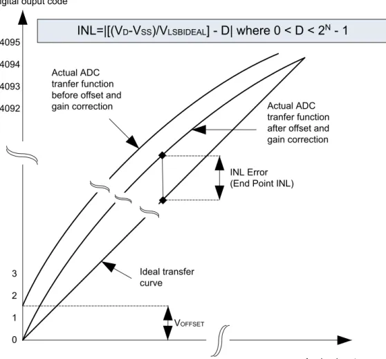
Ideal transfer curve Digital ouput code
Analog Input
INL=|[(V
D-V
SS)/V
LSBIDEAL] - D| where 0 < D < 2
N- 1
0 1 2 3 4092 4093 4094 4095 VOFFSET Actual ADC tranfer function before offset and
gain correction Actual ADC
tranfer function after offset and gain correction INL Error
(End Point INL)
Ideal transfer curve Analog Input 0 1 2 3 4092 4093 Actual transfer function with one missing code.
4 5
0.5 LSB
Ideal Code Center Ideal 50% Transition Point Ideal spacing between two adjacent codes VLSBIDEAL=1 LSB Code width =2 LSB DNL=1 LSB Example: Adjacent input value VD+1 corrresponds to digital output code D+1 Example: Input value
VD corrresponds to
digital output code D
4.11.1 Typical Performance
1.25 V Reference 2.5 V Reference
VDD Reference
Figure 4.16. ADC Frequency Spectrum, VDD = 3 V, Temp = 25 °C
2XVDDVSS Reference 5VDIFF Reference
VDD Reference
1.25 V Reference 2.5 V Reference
VDD Reference
Figure 4.18. ADC Differential Linearity Error vs Code, VDD = 3 V, Temp = 25 °C
2.0 2.2 2.4 2.6 2.8 3.0 3.2 3.4 3.6 3.8 Vdd (V) –4 –3 –2 –1 0 1 2 3 4 5 Actual Offset [LSB] Vref=1V25 Vref=2V5 Vref=2XVDDVSS Vref=5VDIFF Vref=VDD
Offset vs Supply Voltage, Temp = 25 °C
–40 –15 5 25 45 65 85 Temp (C) –1.0 –0.5 0.0 0.5 1.0 1.5 2.0 Actual Offset [LSB] VRef=1V25 VRef=2V5 VRef=2XVDDVSS VRef=5VDIFF VRef=VDD Offset vs Temperature, VDD = 3 V Figure 4.19. ADC Absolute Offset, Common Mode = VDD/2
–40 –15 5 25 45 65 85 Temperature [°C] 63 64 65 66 67 68 SNR [dB] 1V25 2V5 5VDIFF
Signal to Noise Ratio (SNR)
–40 –15 5 25 45 65 85 Temperature [°C] 78.0 78.2 78.4 78.6 78.8 SFDR [dB] 2V5 Vdd 5VDIFF 2XVDDVSS
Spurious-Free Dynamic Range (SFDR) Figure 4.20. ADC Dynamic Performance vs Temperature for all ADC References, VDD = 3 V
–40 –25 –15 –5 5 15 25 35 45 55 65 75 85 Temperature [°C] 2100 2200 2300 2400 2500 2600 Sensor readout Vdd=2.0 Vdd=3.0 Vdd=3.8
4.12 Digital Analog Converter (DAC)
Table 4.16. DAC
Parameter Symbol Test Condition Min Typ Max Unit
Output voltage range VDACOUT VDD voltage reference, single-ended 0 ─ VDD V
VDD voltage reference, differential -VDD ─ VDD V
Output common mode voltage
range VDACCM 0 ─ VDD V
Active current including
refer-ences for 2 channels IDAC
500 kSamples/s, 12 bit ─ 4001 ─ µA
100 kSamples/s, 12 bit ─ 200 ─ µA
1 kSamples/s 12 bit NORMAL ─ 17 ─ µA
Sample rate SRDAC ─ ─ 500 ksamples/s
DAC clock frequency fDAC
Continuous Mode ─ ─ 1000 kHz
Sample/Hold Mode ─ ─ 250 kHz
Sample/Off Mode ─ ─ 250 kHz
Clock cyckles per conversion CYC DAC-CONV
─ 2 ─
Conversion time tDACCONV 2 ─ ─ µs
Settling time tDACSETTLE ─ 5 ─ µs
Signal to Noise Ratio (SNR) SNRDAC
500 kSamples/s, 12 bit,
single-ended, internal 1.25 V reference ─ 58 ─ dB
500 kSamples/s, 12 bit,
single-ended, internal 2.5 V reference ─ 59 ─ dB
500 kSamples/s, 12 bit, differential,
internal 1.25 V reference ─ 58 ─ dB
500 kSamples/s, 12 bit, differential,
internal 2.5 V reference ─ 58 ─ dB
500 kSamples/s, 12 bit, differential,
VDD reference ─ 59 ─ dB
Signal to Noise-pulse
Distor-tion Ratio (SNDR) SNDRDAC
500 kSamples/s, 12 bit,
single-ended, internal 1.25 V reference ─ 57 ─ dB
500 kSamples/s, 12 bit,
single-ended, internal 2.5 V reference ─ 54 ─ dB
500 kSamples/s, 12 bit, differential,
internal 1.25 V reference ─ 56 ─ dB
500 kSamples/s, 12 bit, differential,
internal 2.5 V reference ─ 53 ─ dB
500 kSamples/s, 12 bit, differential,
Spurious-Free Dynamic
Range(SFDR) SFDRDAC 500 kSamples/s, 12 bit, differential,internal 1.25 V reference ─ 61 ─ dBc 500 kSamples/s, 12 bit, differential,
internal 2.5 V reference ─ 55 ─ dBc
500 kSamples/s, 12 bit, differential, VDD reference
─ 60 ─ dBc
Offset voltage V
DACOFF-SET
After calibration, single-ended ─ 2 9 mV
After calibration, differential ─ 2 ─ mV
Differential non-linearity DNLDAC ─ ±1 ─ LSB
Integral non-linearity INLDAC ─ ±5 ─ LSB
No missing codes MCDAC ─ 12 ─ bits
Note:
4.13 Operational Amplifier (OPAMP)
The electrical characteristics for the Operational Amplifiers are based on simulations. Table 4.17. OPAMP
Parameter Symbol Test Condition Min Typ Max Unit
Active Current IOPAMP
(OPA2)BIASPROG=0xF,
(OPA2)HALFBIAS=0x0, Unity Gain ─ 370 460 µA
(OPA2)BIASPROG=0x7,
(OPA2)HALFBIAS=0x1, Unity Gain ─ 95 135 µA
(OPA2)BIASPROG=0x0,
(OPA2)HALFBIAS=0x1, Unity Gain ─ 13 25 µA
Open Loop Gain GOL
(OPA2)BIASPROG=0xF, (OPA2)HALFBIAS=0x0 ─ 101 ─ dB (OPA2)BIASPROG=0x7, (OPA2)HALFBIAS=0x1 ─ 98 ─ dB (OPA2)BIASPROG=0x0, (OPA2)HALFBIAS=0x1 ─ 91 ─ dB
Gain Bandwidth Product GBWOPA MP (OPA2)BIASPROG=0xF, (OPA2)HALFBIAS=0x0 ─ 6.1 ─ MHz (OPA2)BIASPROG=0x7, (OPA2)HALFBIAS=0x1 ─ 1.8 ─ MHz (OPA2)BIASPROG=0x0, (OPA2)HALFBIAS=0x1 ─ 0.25 ─ MHz
Phase Margin PMOPAM
P (OPA2)BIASPROG=0xF, (OPA2)HALFBIAS=0x0, CL=75 pF ─ 64 ─ ° (OPA2)BIASPROG=0x7, (OPA2)HALFBIAS=0x1, CL=75 pF ─ 58 ─ ° (OPA2)BIASPROG=0x0, (OPA2)HALFBIAS=0x1, CL=75 pF ─ 58 ─ °
Input Resistance RINPUT ─ 100 ─ MΩ
Load Resistance1 RLOAD OPA1ALT ─ 1000 ─ Ω
OPA2 ─ 500 ─ Ω
DC Load Current ILOAD_DC ─ ─ 11 mA
Input Voltage VINPUT
OPAxHCMDIS=0 VSS ─ VDD V
OPAxHCMDIS=1 VSS ─ VDD-1.2 V
Output Voltage VOUTPUT VSS ─ VDD V
Input Offset Voltage VOFFSET
Unity Gain, VSS<Vin<VDD,
OPAxHCMDIS=0 -13 0 11 mV
Unity Gain, VSS<Vin<VDD-1.2,
OPAxHCMDIS=1 ─ 1 ─ mV
Input Offset Voltage Drift V OFF-SET_DRIF
(OPA2)BIASPROG=0x0,
(OPA2)HALFBIAS=0x1 ─ 0.1 ─ V/µs
Voltage Noise NOPAMP
Vout=1 V, RESSEL=0, 0.1 Hz<f<10 kHz, OPAxHCMDIS=0 ─ 101 ─ µVRMS Vout=1 V, RESSEL=0, 0.1 Hz<f<10 kHz, OPAxHCMDIS=1 ─ 141 ─ µVRMS Vout=1 V, RESSEL=0, 0.1 Hz<f<1 MHz, OPAxHCMDIS=0 ─ 196 ─ µVRMS Vout=1 V, RESSEL=0, 0.1 Hz<f<1 MHz, OPAxHCMDIS=1 ─ 229 ─ µVRMS RESSEL=7, 0.1 Hz<f<10 kHz, OPAxHCMDIS=0 ─ 1230 ─ µVRMS RESSEL=7, 0.1 Hz<f<10 kHz, OPAxHCMDIS=1 ─ 2130 ─ µVRMS RESSEL=7, 0.1 Hz<f<1 MHz, OPAxHCMDIS=0 ─ 1630 ─ µVRMS RESSEL=7, 0.1 Hz<f<1 MHz, OPAxHCMDIS=1 ─ 2590 ─ µVRMS Note:
1. RLOAD is computed as the delta in measured output voltage at the op-amp output with and without the presence of a 100 µA load.
Figure 4.23. OPAMP Positive Power Supply Rejection Ratio
Figure 4.25. OPAMP Voltage Noise Spectral Density (Unity Gain) Vout = 1 V
4.14 Analog Comparator (ACMP)
Table 4.18. ACMP
Parameter Symbol Test Condition Min Typ Max Unit
Input voltage range VACMPIN 0 ─ VDD V
ACMP common mode
voltage range VACMPCM 0 ─ VDD V
Active current
IACMP
BIASPROG=0b0000, FULL-BIAS=0 and HALFBIAS=1 in
ACMPn_CTRL register
─ 0.1 0.4 µA
IACMPREF
BIASPROG=0b1111, FULL-BIAS=0 and HALFFULL-BIAS=0 in
ACMPn_CTRL register
─ 2.87 15 µA
VACMPOFFSET BIASPROG=0b1111, FULL-BIAS=1 and HALFBIAS=0 in
ACMPn_CTRL register
─ 195 520 µA
Current consumption of internal voltage refer-ence
VACMPHYST Internal voltage reference off.
Us-ing external voltage reference ─ 0 ─ µA
RCSRES Internal voltage reference ─ 5 ─ µA
Offset voltage tACMPSTART BIASPROG= 0b1010,
FULL-BIAS=0 and HALFFULL-BIAS=0 in ACMPn_CTRL register
-12 0 12 mV
ACMP hysteresis Programmable ─ 17 ─ mV
Capacitive sense inter-nal resistance CSRESSEL=0b00 in ACMPn_IN-PUTSEL ─ 39 ─ kΩ CSRESSEL=0b01 in ACMPn_IN-PUTSEL ─ 71 ─ kΩ CSRESSEL=0b10 in ACMPn_IN-PUTSEL ─ 104 ─ kΩ CSRESSEL=0b11 in ACMPn_IN-PUTSEL ─ 136 ─ kΩ Startup time ─ ─ 10 µs
The total ACMP current is the sum of the contributions from the ACMP and its internal voltage reference as given below. IACMPREF is zero if an external voltage reference is used: IACMPTOTAL = IACMP = IACMPREF
0 4 8 12 ACMP_CTRL_BIASPROG 0.0 0.5 1.0 1.5 Current [uA]
Current Consumption, HYSTEL = 4
0 2 4 6 8 10 12 14 ACMP_CTRL_BIASPROG 0.0 0.5 1.0 1.5 2.0 2.5 3.0
Response Time [us]
Response Time 0 1 2 3 4 5 6 7 ACMP_CTRL_HYSTSEL 0 20 40 60 80 100 Hysteresis [mV] BIASPROG=0.0 BIASPROG=4.0 BIASPROG=8.0 BIASPROG=12.0 Hysteresis
4.15 Voltage Comparator (VCMP)
Table 4.19. VCMP
Parameter Symbol Test Condition Min Typ Max Unit
Input voltage range VVCMPIN ─ VDD ─ V
VCMP Common Mode
voltage range VVCMPCM ─ VDD ─ V
Active current IVCMP
BIASPROG=0b0000 and
HALF-BIAS=1 in VCMPn_CTRL register ─ 0.3 0.6 µA
BIASPROG=0b1111 and HALF-BIAS=0 in VCMPn_CTRL register.
LPREF=0.
─ 22 35 µA
Startup time reference
generator tVCMPREF NORMAL ─ 10 ─ µs
Offset voltage VVCMPOF
FSET single-ended ─ 10 ─ mV Differential ─ 10 ─ mV VCMP hysteresis VVCMPHY ST ─ 61 210 mV Startup time tVCMPST ART ─ ─ 10 µs
The VDD trigger level can be configured by setting the TRIGLEVEL field of the VCMP_CTRL register in accordance with the following equation: VDD Trigger Level=1.667 V+0.034 ×TRIGLEVEL