熊本大学学術リポジトリ
Evaluation of BJTs as Closing Switch of Miniaturized Marx Generator
journal or
publication title
Digest of Technical Papers‑IEEE International Pulsed Power Conference
volume 2007
page range 468‑471
year 2007‑06
URL http://hdl.handle.net/2298/10314
doi: 10.1109/PPPS.2007.4345667
EVALUATION OF BJTs AS CLOSING SWITCH OF MINIATURIZED MARX GENERATOR
C. Yamada, T. Ueno, T. Namihira, T. Sakugawa, S. Katsuki and H. Akiyama
Graduate School of Science and Technology, Kumamoto University, 2-39-1 Kurokami, Kumamoto 860-8555, JAPAN
Abstract
The micro plasma technology is used in various fields such as processing or chemical analysis of minute material, short-wavelength light source, and plasma function device. The plasmas can be generated by an electric discharge. The miniaturized generator was used to produce these plasmas in the micro-scale area. For such background, the miniaturized Marx generator which has Bipolar Junction Transistors (BJTs) as closing switches was developed to generate micro plasmas. In the miniaturized Marx generator, BJTs were operated in avalanche mode to obtain a faster switching speed with ns order. In this paper, three kinds of BJTs which have different collector current each others were evaluated as closing switch. In the experiment, the BJTs were operated in avalanche mode with higher applied voltage (about twice voltage rating) into the between collector and emitter of BJTs. As the result, as Vc increases, the switching time of BJTs which operated in the avalanche mode was decreases. And, the peak of Ic of three kinds of BJTs which operated in avalanche mode was almost same.
I. INTRODUCTION
The micro-plasma has gotten a lot of attention recently, because it can be used for the various applications. The micro plasma is used for chemical analysis or process, short wavelength light source, and the plasma function device. In the field of the micro plasma, the power supply and the system should not be large-scale. Hence, the pulsed power source that part of micro-plasma generating system has been miniaturized.
For such background, the miniaturized Marx generator that uses bipolar junction transistors (BJTs) which operated in avalanche mode as closing switch has been completed in this laboratory. However, the output energy of miniaturized Marx generator is insufficient for the micro plasma generation. Therefore, the output power of miniaturized Marx generator should be large. For such reason, to increase the output energy of miniaturized Marx generator, the BJTs as switching device of miniaturized Marx generator was evaluated.
II. EVALUATION CIRCUIT OF BJT SWITCHING
Figure 1 shows the evaluation circuit of BJT switching.
The circuit consisted of a charging resistor (R
ch=20 kΩ), a BJT, a capacitor and TTL signal generator. In this work, three BJTs, named 2SC2655, 2SC5076 and 2SC5000 (NPN type Bipolar Junction Transistor, Toshiba, Japan), were evaluated as a closing switch. On the specification sheets of each BJT, three BJTs, used in this work, have the same corrector-emitter voltage (V
CEO) of 50V and have the different corrector current (I
C). The I
Cs of 2SC2655, 2SC5076 and 2SC5000 BJTs are 2, 5 and 10 A, respectively. For the evaluation of BJTs, the capacitor was carried from 0.015 to 1.000 µF. In the evaluation, the capacitor was charged up to set-up voltage (V
C) by DC power source (V
CH, Cockroft-Walton's circuit, handmade) through the charging resistor. The TTL signal from generator (33220A, Agilent, USA) was applied between the base and the emitter of BJT at 3 pps (Pulsed per second). The V
Cand I
Cwere measured by the high voltage probe (PHV641, PMK, Germany) which is connected between the corrector and the emitter of BJT and the current transformer (Model 2877, Pearson Electronics, USA) which is located on the emitter of BJT (ground), respectively. The signal from the measurement devices were recorded by the digital storage oscilloscope (TDS3034B, Tektronix, USA).
Figure 1. Evaluation circuit of BJT as closing switch.
A. Onset voltage of leakage current
Figure 2 shows the dependence of V
Con V
chin the case
of using 2SC2655 BJT. The Vc increased linearly with
the V
chin the range of 0 to 160 V. Over 170 V of the V
ch,
the V
Creduced from V
ch. This means that the leakage
current in the evaluation circuit started flowing when the
V
chreached at 170V. In the case of other BJTs (2SC5076
and 2SC5000), the onset voltage of the leakage current
flowing were 200 V, respectively. From the results, the evaluations of BJTs were carried out in the range from 0 to the onset voltage of leakage current of V
C.
Figure 2. Dependence of V
Con V
ch. BJT: 2SC2655.
B. Voltage and current waveforms as switching Figure 3 shows the typical V
Cand I
Cwaveforms in the case of using 2SC2655 BJT and 0.1 µF of the capacitor.
Figure 3 (a) indicates the waveforms in the operation with 50 V of V
C. On the other hand, Figure 3 (b) indicates the waveforms in the operation with 140 V of V
C. It is observed from Figure 3 (a) that the V
Cfell down from 50 to 0 for 0.5 µs. The peak of I
Climited lower than 6 A which is 3 times of specified I
C. Here, it is noted that the switching time was defined as the time duration of the voltage fall time from 90 % to 10 % of V
C. From Figure 3 (a), the switching time of 2SC2655 BJT was 500 nanoseconds. From Figure 3 (b), the V
Cfell down from 140 to 0 for 0.15 µs. The peak of I
Cis 90 A which is 45 times of specified I
C. The switching time of 2SC2655 BJT was 120 nanoseconds.
Figure 4 shows the I
Cwaveform in the case of using 2SC5000 BJT and 0.1µF of the capacitor for three different V
C. It is shown from Figure 4 that operation mode of BJT shifts from normal mode to avalanche mode when I
Cexceeds the threshold current. The maximum threshold current of BJTs are 7A, 15A and 30A, respectively. This threshold current is about 3 times of specified I
C. And this threshold current is different depending on the V
C. As V
Cincrease, rise time of I
Cis fast, so I
Cexceeds the threshold current fast.
C. Current characteristic
Figure 5 shows the current characteristic as a function of the V
Cin the case of using 2SC2655 BJT. In normal mode operation, I
Cis limited by the specification of I
C. In avalanche mode operation, I
Cincreased fast. I
Cof BJT which operated in avalanche mode operation as closing switch was given by
L V C
I
C=
C(1)
-10 0 10 20 30 40 50 60
-10 0 10 20 30 40 50 60
0 0.5 1 1.5 2
Vc[V] Ic[A]
Vc , V Ic , A
Time, µs (a)
-50 0 50 100 150 200
-50 0 50 100 150 200
0 0.5 1 1.5 2
Vc[V] Ic[A]
Vc, V Ic, A
Time, µs (b)
Figure 3. Capacitor voltage waveform (Vc) and collector current waveform (Ic). (a) When BJT was operated in normal mode. (b) When BJT was operated in avalanche mode.
Figure 4. Collector current waveform for three different Vc (2SC5000, C=0.100uF).
469
where C is capacitance, and L is circuit inductance. This relational expression is clear from Figure 5. Because, in avalanche mode operation, I
Cis proportional to V
Cor square root C. Another characteristic in this test, V
Cdecreases when the capacitor increases. This is clear from that the threshold to shift to avalanche mode operation is almost constant and the equation (1).
Figure 6 shows the comparison of the current characteristic as a function of V
C. When BJT was operated in normal mode operation, I
Cof each BJT has the 5 times difference. However, in avalanche mode operation, I
Cof each BJT is almost same. Hence, the specification of I
Cis not important to use BJT as switching device of Marx generator.
0 50 100 150 200 250 300 350
0 50 100 150 200
0.100uF 0.470uF 1.000uF
pea k of Ic , A
Vc, V
Figure 5. Current characteristic as a function of Vc.
0 50 100 150 200 250 300 350
0 50 100 150 200
2SC2655 2SC5076 2SC5000
pea k of Ic , A
Vc, V
Figure 6. Comparison of the current characteristic as a function of Vc.
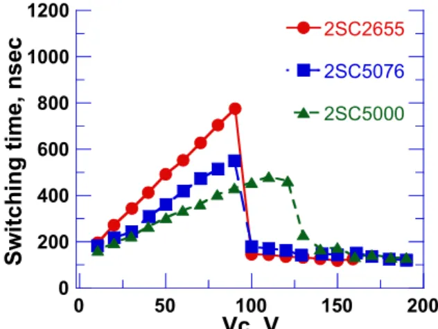
D. Switching time characteristic
Figure 7 shows the switching time characteristic as a function of the V
Cin the case of using 2SC2655 BJT. In normal mode operation, as V
Cand C increase, the switching time is increased. In this case, I
Cthat flow in the BJT is limited by the specification of I
C. Therefore, when the quantity of electric charge (Q=V
CC) is large, the switching time is increased.
In avalanche mode operation, as capacitance is increased, the switching time is increased. However, the switching time is increased as V
Cdecreases. As discussed previous, I
Cexceeds the threshold current fast as the voltage is high, and then it shifts into avalanche mode operation.
Figure 8 shows the comparison of the switching time characteristic as a function of the V
C. It is shown from figure 8 that 2SC2655 is the faster than other BJTs.
Because the specification of I
C2SC2655 is smaller than another BJTs, its threshold current that shifts into avalanche mode is most small. Hence, 2SC2655 shifts into avalanche mode fast. In a word, the switching time is fast. The difference of this shift time greatly influences the switching time characteristic. Because the delay to avalanche mode operation of 2SC2655 is most small, it is the suitable as the switching device in the Marx generator.
0 1000 2000 3000 4000 5000 6000 7000
0 50 100 150 200
0.100uF 0.470uF 1.000uF
Sw itc h in g ti m e, n sec
Vc, V
Figure 7. Switching time characteristic as a function of Vc.
0 200 400 600 800 1000 1200
0 50 100 150 200
2SC2655 2SC5076 2SC5000