Adjacent Channel Interference Mitigation Schemes for Software Defined Radio Receiver
July 2008
Anas Bin Muhamad Bostamam
DISSERTATION
Submitted to the School of Integrated Design Engineering, Keio University,
in partial fulfillment of the requirements for the degree of Doctor of Philosophy
Copyright c 2008 by Anas Bin Muhamad Bostamam All right reserved
Contents
1 General Introduction 5
1.1 The Need for Reconfigurable Radio Architectures . . . 5
1.2 Software Defined Radio . . . 6
1.3 Receiver Architectures . . . 8
1.3.1 Superheterodyne Receiver . . . 9
1.3.2 Direct Conversion Receiver . . . 11
1.3.3 Low-IF Receiver . . . 12
1.3.4 RF-Sampling Receiver . . . 14
1.4 Sampling in ADC and Sample Rate Conversion . . . 16
1.4.1 Nyquist Sampling . . . 17
1.4.2 Oversampling . . . 20
1.4.3 Undersampling . . . 21
1.4.4 Sample Rate Conversion . . . 22
1.5 Adjacent Channel Interference . . . 25
1.5.1 Out-of-band Side-lobe Energy . . . 27
1.5.2 ACI due to Undersampling . . . 28
1.5.3 Aliasing due to Sample Rate Conversion . . . 29
1.6 Motivation of the Research . . . 30
1.6.1 Realization of SDR receiver . . . 30
1.6.2 Adjacent Channel Interference Cancellation Scheme for Low-IF
Receiver in Multi-Channel Reception . . . 35
1.6.3 Undersampling for Adjacent Channel Interference Cancellation Scheme . . . 37
1.6.4 Fractional Sample Rate Conversion for SDR . . . 39
2 Adjacent Channel Interference Cancellation Scheme for Low-IF Re- ceiver in Multi-Channel Reception 41 2.1 Introduction . . . 41
2.2 Multi-Channel Reception . . . 43
2.2.1 Roaming Protocol . . . 43
2.2.2 Multi-Channel Reception with Low-IF Architecture . . . 46
2.3 System Model . . . 48
2.4 Experiment System . . . 52
2.5 Experiment Results . . . 56
2.6 Conclusion . . . 64
3 Undersampling in Multi-channel Reception Scheme 66 3.1 Introduction . . . 66
3.2 Multi-Channel Reception . . . 69
3.2.1 Roaming Protocol . . . 69
3.2.2 Multi-Channel Reception with Low-IF Architecture . . . 69
3.2.3 Adjacent Channel Interference (ACI) . . . 71
3.2.4 ACI Cancellation with Undersampling . . . 72
3.3 System Model . . . 73
3.4 Experiment Results . . . 76
3.4.1 Experiment System . . . 76
3.4.2 Characteristics of the Analog Complex Filters . . . 80
3.4.3 BER Performance . . . 82
3.5 Conclusion . . . 86
4 Direct Insertion/Cancellation method based Fractional Sample Rate Conversion for Software Defined Radio 89 4.1 Introduction . . . 89
4.2 Conventional Direct Insertion/Cancellation SRC Method . . . 92
4.3 Proposed Method . . . 94
4.4 Analytical Calculation for Sinusoidal Signal . . . 98
4.5 Numerical Results . . . 102
4.5.1 Analysis and Simulation with Sinusoidal Signal . . . 102
4.5.2 Implementation Example . . . 108
4.6 Conclusions . . . 114
5 Overall Conclusions 116
Acknowledgement 126
List of Papers by Author 128
List of Figures
1.1 Wireless standards. . . 6
1.2 Ubiquitous wireless communications with SDR. . . 7
1.3 Ideal SDR concept . . . 9
1.4 ADC architecture, application,resolution and sampling rates. . . 9
1.5 Superheterodyne receiver architecture. . . 10
1.6 Direct conversion receiver architecture. . . 11
1.7 Downconversion in DCR. . . 11
1.8 Low-IF receiver architecture. . . 13
1.9 Down conversion of the received signal in low-IF receiver architecture. 13 1.10 RF-sampling receiver architecture. . . 15
1.11 Block diagram of the DTR by TI. . . 16
1.12 Spectral characteristics of Nyquist sampling. . . 17
1.13 Spectral characteristics of fs< fN yquist. . . 19
1.14 Spectral characteristics of oversampling, OSR=2. . . 19
1.15 Spectral characteristics of undersampling. . . 21
1.16 Frequency conversion with undersampling. . . 22
1.17 Rational Factor SRC . . . 24
1.18 Direct insertion/cancellation based fractional-SRC. . . 25
1.19 Generated images after direct insertion/cancellation. . . 26
1.20 Interference due to the signal in the adjacent channel. . . 27
1.21 IEEE 802.11a channel spectrum. . . 28
1.22 Spectrum mask standard and spectrum of amplifier output. . . 29
1.23 ACI due to the undersampling . . . 30
1.24 ACI due to the direct insertion/cancellation SRC. . . 30
1.25 Ideal SDR concept . . . 32
1.26 Superheterodyne receiver architecture. . . 33
1.27 DCR architecture. . . 33
1.28 Low-IF receiver architecture. . . 34
1.29 RF-sampling receiver architecture. . . 34
1.30 Motivation of the research. . . 35
1.31 Relationship of the research about ACI cancellation in Low-IF receiver architectures. . . 36
1.32 Relationship of the research on fractional SRC. . . 40
2.1 Roaming example with IEEE802.11 MAC Protocol. . . 43
2.2 Passive scan. . . 44
2.3 Active scan. . . 45
2.4 Seamless handover using two WLAN devices on a mobile node. . . 46
2.5 Low-IF receiver architecture. . . 46
2.6 Downconversion of the received signal in low-IF receiver architecture. 47 2.7 Downconversion of multi-channel and interference due to the signal in the adjacent channel. . . 48
2.8 Model of the receiver with the proposed scheme. . . 48
2.9 Received signal model. . . 49
2.10 Wiener filter model. . . 50
2.11 Model of the experiment system. . . 52
2.12 Model of the analog filter. . . 53
2.13 Single complex pole with active-RC filter. . . 54
2.14 Normalize characteristic of the H0 analog filter. . . 56
2.15 Normalize characteristic of the H1 analog filter. . . 56
2.16 Input of the analog filters, SIR=0[dB] 64carrier QPSK/OFDM signal. 57 2.17 Output of H0, SIR=0[dB] 64carrier QPSK/OFDM signal. . . 58
2.18 Input of the analog filters, SIR=-12[dB] 64carrier QPSK/OFDM signal. 58 2.19 Output of H0, SIR=-12[dB] 64carrier QPSK/OFDM signal. . . 59
2.20 SIR=-12[dB],SNR=20[dB],Spectrum of (a)Y0(b)Y1(c)Reference signal,s, (d)Output of Wiener filter,d . . . 60
2.21 BER vs. Number of coefficient, SNR=10[dB]. . . 61
2.22 Estimated coefficients. . . 61
2.23 BER vs. SIR, SNR=10[dB], resolution [8bits]. . . 62
2.24 BER vs. SNR, SIR=-12[dB], resolution 8[bits]. . . 63
2.25 BER vs. Resolution of ADC, SIR=-12[dB], SNR=10[dB]. . . 64
3.1 Roaming example with IEEE802.11 MAC Protocol. . . 67
3.2 Low-IF receiver architecture. . . 70
3.3 Downconversion of multi-channel and interference due to the signal in the adjacent channel. . . 71
3.4 4 bands of WLAN after downconversion with low-IF receiver. . . 71
3.5 Model of the receiver with the proposed scheme. . . 73
3.6 Signal model. . . 74
3.7 Model of the experiment system. . . 77
3.8 Model of the analog filter. . . 78
3.9 Single complex pole with active-RC filter. . . 79
3.10 Normalized characteristic of the H0 analog filter. . . 80
3.11 Normalized characteristic of the H2 analog filter. . . 81
3.12 Received signal, SIR=-12[dB]. . . 81
3.13 (a) Output ofH0BPF,fs=10[MHz] (b) Output ofH2BPF,fs=10[MHz]
(c) Output ofH0BPF,fs=2.5[MHz] (d) Output ofH2BPF,fs=2.5[MHz].
82
3.14 Signal without interference, resolution of ADC = 8[bits]. . . 83
3.15 BER vs. the number of coefficients, SIR=-18[dB], SNR=6[dB] , reso- lution of ADC = 8[bits]. . . 83
3.16 BER vs. SNR, SIR=-12[dB], resolution of ADC = 8[bits]. . . 84
3.17 BER vs. SIR, SNR=6[dB], resolution of ADC = 8[bits]. . . 85
4.1 Direct insertion/cancellation based fractional-SRC. . . 92
4.2 Aliasing due to the Direct insertion/cancellation method. . . 94
4.3 Proposed method. . . 95
4.4 Output of 6/5-ratio SRC. . . 96
4.5 Output of 4/5-ratio SRC. . . 97
4.6 Phase difference between the converted signal and the target signal, insertion period N=5, insertion phase R=5. . . 100
4.7 MSE simulation model for sinusoidal signal. . . 103
4.8 MSE results vs. input signal frequency, sample rate 300MHz→360MHz.104 4.9 MSE results vs. number of set, sample rate 300MHz→ 360MHz. . . . 105
4.10 MSE results vs. input signal frequency, sample rate 300MHz→240MHz.106 4.11 MSE results vs. number of set, sample rate 300MHz → 240MHz. . . . 107
4.12 Power spectrum of 8.125MHz sinusoidal signal, sample rate 300MHz →360MHz. . . 107
4.13 Pulse waveform: simulation results: MSE results vs. number of set, sample rate 300MHz →360MHz. . . 108
4.14 Pulse waveform: simulation results: BER results vs. Eb/N0, sample rate 300MHz → 360MHz. . . 109
4.15 Simulation model for OFDM signal . . . 110
4.16 Power spectrum of OFDM signal, sample rate 300MHz → 360MHz. . 111
4.17 BER vs. Eb/N0, QPSK-OFDM. . . 112
4.18 BER vs. Eb/N0, 16QAM-OFDM. . . 112
4.19 ACI due to the direct insertion. . . 113
4.20 BER vs. Eb/N0, QPSK-OFDM, SIR=-10[dB]. . . 114
4.21 BER vs. SIR, QPSK-OFDM, Eb/N0=8[dB]. . . 115
List of Tables
2.1 Experiment Conditions . . . 52
2.2 Characteristics of the analog filters. . . 57
3.1 Experiment Conditions. . . 77
3.2 Characteristics of the analog filters. . . 81
4.1 Simulation conditions for sinusoidal signal. . . 102
4.2 Simulation conditions for general pulse waveform signal. . . 108
4.3 Simulation conditions for OFDM signal . . . 110
4.4 Simulation MSE results for OFDM . . . 111
Abstract
Wireless communication technology such as cellular and wireless local area network (WLAN) systems have grown rapidly and generated various competing transmission formats. In the need of seamless communication across incompatible radio standards, software defined radio (SDR) concept has received much attention among researchers working in mobile and personal wireless communications. SDR is a technology that allows a single terminal to support various kinds of wireless systems and services such as mobile systems and WLANs by changing software to reconfigure the wireless ter- minal. In order to realize a SDR receiver, flexible receiver architecture with wideband signal receiving capability is required. However, if the receiving bandwidth is wider, the received signal components may cause interference to each other. In this study, the signal processing methods to combat the adjacent channel interference (ACI) problems in the SDR receivers are investigated and discussed.
In this dissertation, we use 2 approaches to realize the flexible receiver for SDR;
1. Low-IF signal mixing downconversion receiver architecture 2. RF sampling receiver architecture
In the low-IF receiver, received radio frequency (RF) signal is mixed down to a non- zero low or moderate intermediate frequency (IF). The low-IF receiver is superior to conventional superheterodyne receiver as the architecture does not require exter- nal filter. The low-IF receiver does not suffer much from its non-idealities, such as DC-offset and 1/f noise problems in direct-conversion receiver (DCR). In the RF sam- pling receiver architecture, the received signal is sampled at a RF and is processed
directly at the analog domain. The downconversion technique in the RF sampling is based on current sampling, which greatly simplifies the mixer circuit design. These architectures achieve reduction of off-chip components and enable the realization of a one-chip receiver.
This dissertation is focusing on signal processing methods to combat ACI problems in The SDR receiver. In the 2nd chapter, the interference from the mirror frequency in a multi channel low-IF receiver is discussed. In the wideband low-IF receiver, a high resolution analog-to-digital converters (ADCs) should be employed to accommodate signals with a very large dynamic range. Moreover, the ACI component may directly overlap with the desired signal if the interference is much larger than the desired signal. In the 3rd chapter, the effect of ACI due to undersampling to the multi channel low-IF receiver is investigated and discussed. The 4th chapter investigate the methods to mitigate the ACI effect due to a sample rate conversion in an RF- sampling receiver.
Chapter 1 introduces the background of the SDR and the motivation of the re- search.
In Chapter 2 a new ACI cancellation scheme for multi-channel signal reception with low-IF receivers is investigated through the experiment. In the low-IF receivers, the signal in the mirror frequency causes interference to the desired signal. A high resolution ADCs should be employed to accommodate signals with a very large dy- namic range. Moreover, the ACI component may directly overlap with the desired signal if the interference is much larger than the desired signal. In order to reduce the required resolution of the ADCs and reduce the interference, an analog-digital signal processing technique has been investigated . This technique uses a band pass filter (BPF) for each WLAN channel. The BPFs ease the dynamic range of ADCs and enables multi-channel demodulation with low resolution ADCs. Nevertheless, the problem of the analog BPFs is that it cannot eliminate the interference completely
due to the restriction of the circuit size and the mismatch of the analog components.
In the proposed analog-digital signal processing scheme, channel selection is made by analog complex band pass filter and the signal is reconstructed by Wiener filter to eliminate the interference effect in order to improve the performance.
In Chapter 3 an ACI cancellation scheme with undersampling for multi-channel reception is proposed and investigated. The main objective of Chapter 3 is to improve the system that has been proposed in Chapter 2 by reducing the ADC sample rate requirement. Undersampling technique is applied in this system in order to reduce the required sampling frequency and power consumption. However, the undersam- pling technique requires high performance BPFs to minimize the out-of-band signals, otherwise, the out band signal will be aliased and translated to the desired band.
The effects of the adjacent channel to the undersampling technique in this scheme is examined and discussed in the chapter. In the proposed scheme, the influence of the undersampling side effect is reduced by the Wiener filter.
Chapter 4 proposes a new fractional sample rate conversion (SRC) scheme for the RF-sampling receiver architecture. This scheme is suitable for signals that are sampled at a high sample rate and converted to a lower sample rate. The objective of the scheme is to realize a high-speed and high-performance SRC scheme with low- complexity and lower power consumption. High-speed SRC scheme for high sample rate data can be realized by a direct insertion/cancellation scheme. This technique is suitable for application in the RF sampling receiver which samples data with a high oversampling ratio (OSR). However, the direct insertion/cancellation technique suffers from large aliasing and distortion as compared to the other SRC techniques.
The aliasing from an adjacent channel interferes the desired signal and degrades the performance. Moreover, the aliasing from the adjacent channel interferes the desired signal. Therefore, a modified direct insertion/cancellation scheme is proposed in order to realize high performance resampling. The distortion noise or aliasing can be
reduced by applying multiple branches of parallel inserters/deleters. This proposed scheme mitigates the ACI, reduces the required complexity of an anti-aliasing filter structure, and improves the performance.
Finally, Chapter 5 summarizes the results of each chapter and conclude this thesis.
Chapter 1
General Introduction
In this chapter, first, we introduce the concepts of software defined radio (SDR).
Then we present the receiver architectures that has been proposed for SDR. After that, we show some sampling concept in ADCs and sample rate conversion (SRC).
Then, the issues related to the adjacent channel interference (ACI) in the receiver architecture are presented. Finally, the motivation of the research is presented in the final section. The section also explains the relationship among each chapter and the historical background of each chapter.
1.1 The Need for Reconfigurable Radio Architec- tures
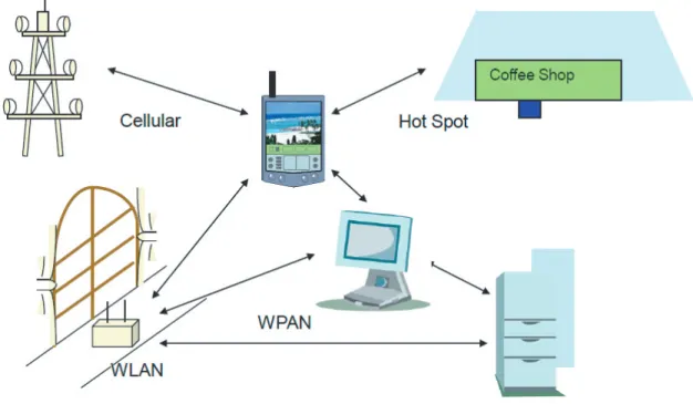
Wireless communication is now routinely used for a large variety of applications including voice, data transfer, Internet access, audio and video streaming. Due to the demand for bandwidth and the steady improvement of semiconductor technology, the performance offered by wireless standards is improving rapidly every years, seemingly without bounds, as illustrated in Fig. 1.1. The observed and predicted evolution of the main classes of wireless standards is indicated as thick arrows (from bottom to top): wireless personal area networks (WPAN), wireless local area networks (WLAN), wireless metropolitan area networks (WMAN), and cellular networks.
Figure 1.1: Wireless standards.
Future communications systems will have to seamlessly and opportunistically in- tegrate these multiple radio technologies. In the future communications systems, a single handheld device that can support a large number of these wireless standards enabling ubiquitous connectivity through seamless horizontal and vertical handovers.
This is supported by SDRs, which use a common hardware platform for different standards [1, 2].
1.2 Software Defined Radio
Wireless communication technology such as cellular and WLAN systems have grown rapidly and generated various competing transmission formats. In the need of seam- less communication across incompatible radio standards, SDR concept has received much attention among researchers working in mobile and personal wireless commu- nication. SDR is a technology that allows a single terminal to support various kinds of wireless systems and services such as mobile systems and WLANs by changing software to reconfigure the wireless terminal [1–3]. SDR technology enables ubiqui-
Figure 1.2: Ubiquitous wireless communications with SDR.
tous data connectivity by supporting multi-band and multi-mode wideband wireless terminal, as illustrated in Fig. 1.2. Seamless communication could be possible by selecting the wireless system that best corresponds to the communication environ- ment and user’s requirements. Desired quality of service can be maintained while improving service economy based on the data-rate and communication fee, etc.
There are several merits by using SDR technology. One terminal can be used for various wireless systems such as cellular, WLAN, WMAN, WPAN, TV, ITS, GPS, etc. New services can be provided and obtained by software version upgrade without replacing infrastructures and terminals. Therefore, there are no need to replace all terminals when new services is launched. In-service systems can be remotely main- tained. The development period will be shorten because there are no longer need to develop specific chips for each system.
In order to realize the SDR terminal, radio frequency (RF) circuit that support multi-band signal, flexible baseband signal processing to support multi-band, multi-
standard and multi-mode system, and high resolution high speed analog-to-digital converter (ADC) to counter fading and ACI, are needed. The combination of the flexibility of signal processing with RF circuitry to allow software to dynamically control communications parameters such as carrier frequency, bandwidth, power lev- els, and data rate. In addition, the software at the heart of the systems can perform functions such as filtering signals, establishing modulation and coding schemes, and determining frequency-hopping patterns.
1.3 Receiver Architectures
The ideal concept for the SDR terminal is to attach an ADC directly to the antenna such as shown in Fig. 1.3 [1]. However, the ideal scheme is not completely realizable due to the actual technology limits; especially the need of ultra high speed ADC cannot be realized by the current technology.
Figure 1.4 shows current ADC architectures with their resolution and sampling rate. At sampling rates below 2MHz, resolution appears to be limited by thermal noise. At sampling rates ranging from 2MHz to 4GHz, resolution falls off by 1 bit for every doubling of the sampling rate. This behavior may be attributed to uncertainty in the sampling instant due to aperture jitter. For ADCs operating at multi-GHz rates, the speed of the device technology is also a limiting factor due to comparator ambiguity [4]. Many ADC architectures and integrated circuit technologies have been proposed and implemented to push back these limits. The trend toward single-chip ADCs brings lower power dissipation. However, technological progress as measured by the product of the ADC resolution (bits) times the sampling rate is slow. Even the ADC technology grows, it is still far from the requirement of the ideal SDR terminals.
Therefore, trade-offs between the ideal SDR and the available technology must be made. The actual practical solution is to let the software processing stage be preceded
Figure 1.3: Ideal SDR concept
Figure 1.4: ADC architecture, application,resolution and sampling rates.
by a front-end that preconditions the input signals to give them characteristics that enable the subsequent stage to elaborate them.
1.3.1 Superheterodyne Receiver
A superheterodyne RF front end architecture is adopted to lower the frequency of the received signals to intermediate frequency (IF) values. The superheterodyne receiver, which was introduced by Armstrong in 1918 [5], has been used in radio and television receivers and transmitters in order to tune them to a particular frequency.
A typical structure of the superheterodyne receiver architecture, consists of a RF filter, low noise amplifier (LNA), multiple down-conversion mixers, off-chip passive
Figure 1.5: Superheterodyne receiver architecture.
image rejection filter, and variable-gain amplifier (VGA), as illustrated in Fig. 1.5.
The superheterodyne receiver downconverts the received RF signal to a fixed IF, by mixing all of the incoming signals with an internally generated waveform, using a single mixer and tunable local oscillator (LO). In the mixer stage of a receiver, the LO signal multiplies with the incoming signals, which shifts them all down in frequency.
After the down-conversion mixer, a passive off-chip channel select filter attenuates the out-of-channel signals to a sufficiently low level. A VGA, which follows the IF channel-select filter, decreases the dynamic range requirements of the ADC. Then, the desired signal is downconverted to the baseband before it is converted to a digital signal by an ADC.
A super-heterodyne receiver heavily relies on expensive external, high-Q passive filter to perform the mirror signal suppression and the channel selection [6]. These high-Q filters cannot be integrated on silicon because the power consumption of ac- tive filter is proportional to the the square of its quality-factor. These filters usually realized with off-chip surface acoustic wave (SAW) filter. Although the filtering func- tions themselves do not consumed any power, the input and output of each off-chip filter requires impedance matching that increases the power consumption in the RF front-end. Although the off-chip filters offer sufficient image rejection and selectivity, the superheterodyne implementation of a multimode receiver with such filters will not only increase the production cost but also the physical dimension of the handset.
Figure 1.6: Direct conversion receiver architecture.
Figure 1.7: Downconversion in DCR.
Thus, superheterodyne receiver is not a practical topology for multimode receiver designs.
1.3.2 Direct Conversion Receiver
Direct conversion receiver (DCR) architecture, which has introduced the zero IF approach, supports efficient wireless terminal designs with a high level of integration [7,8]. In the DCR, the desired signal downconverted directly to baseband signal with only single conversion stage. The elimination of components and processing in IF stage had greatly lower complexity and power consumption in the DCR architecture.
The receiver, shown in Fig. 1.6 [6], consists of a RF filter, LNA, quadrature down- conversion mixers, low-pass filters (LPFs), and VGAs. The RF filter attenuates the
out-of-band signals before the LNA. The architecture uses quadrature modulation, two down-conversion mixers are required to avoid an unrecoverable loss of informa- tion. The LO signals of the two mixers have a phase shift of 90◦ which produces the in-phase (I) and quadrature (Q) components. There are no need for an off-chip filter in the DCR architecture, since both the mirror signal and the noise will eventually be neutralized by the recombination of the two signal paths after the quadrature down-conversion. After the downconversion mixers, the signal is at baseband where the channel selection is performed by integrated LPFs. Following, VGAs are utilized to amplify the baseband signal to a suitable level.
The downconversion is done in a single step in two signal path, instead of a cascade of mixing stages, as illustrated in Fig. 1.7. Further signal processing such as image rejection demodulation of the signal is carried out in the digital domain by a DSP. This is an attractive property, since the digital domain features a much better scalability and a great flexibility.
However, there are direct current (DC) offset and 1/f noise problems in the archi- tecture [7, 9]. The offset arises from the self-mixing of the LO and the self-mixing of undesired interferer in the preselect filter passband. The DC offset, which appears in the middle of the downconverted signal spectrum, and may be larger than the signal itself, and much larger than thermal and 1/f noise. The DC offset will reduce the signal-to-noise ratio (SNR) at the detector input and degraded the performance. The 1/f noise or flicker noise is an intrinsic phenomenon found in semiconductor devices.
the 1/f noise, which has spectral density that is inversely proportional to frequency, distort the signal that is nearer to the DC.
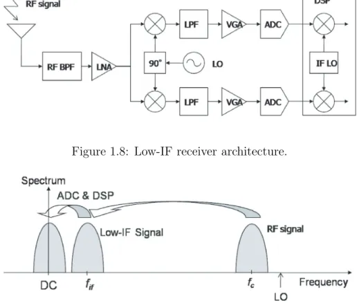
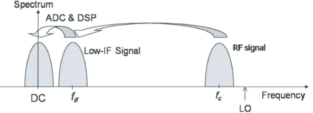
1.3.3 Low-IF Receiver
Low-IF receiver architecture has been proposed to avoid DC offset and 1/f noise problems in the DCR [10]. In a low-IF receiver, the RF signal is mixed down to a
Figure 1.8: Low-IF receiver architecture.
Figure 1.9: Down conversion of the received signal in low-IF receiver architecture.
non-zero low or moderate intermediate frequency, typically a few megahertz. The structure of the low-IF receiver is shown in Fig. 1.8. Received signal through antenna goes through band-pass filter. A broadband RF filter is used to prevent overloading of the mixers with strong out of band signals. The LNA amplifies the weak signal from antenna to a sufficient SNR. In low-IF receiver architecture, the received signal is down converted to the IF signal by mixing the signal with LO, such is shown in Fig. 1.9. Then the IF signal is converted to digital signal with ADCs and finally converted to the baseband signal using DSP. As the down conversion is carried out with DSP, channel selection can be done easily.
The advantages of this topology consists in the high level of integration and the lack of DC offsets as in the case of zero IF receiver. DC can be easily decoupled after
down conversion. The second IF is at low frequency and digital signal processing is possible. Low-IF receivers are not using SAW filter so that this architecture would have low cost and low power consumption as compared to super-heterodyne archi- tecture. The low-IF receiver is much easier to make in one chip and the structure of the low-IF receiver can be much simpler than the super-heterodyne receiver.
Receiver system with the low-IF receiver architecture is described in Chapter 2 and 3.
1.3.4 RF-Sampling Receiver
Direct RF-Sampling Receiver
The RF-sampling receiver scheme has been proposed recently to replace the con- ventional mixer-based downconversion scheme. The direct RF sampling technique is based on current sampling, which greatly simplifies the mixer circuit design. In the RF-sampling architecture, the received signal is processed directly at the analog domain and sampled at the RF [11, 12]. Channel selection and demodulation are carried out in the digital domain [13]. This architecture achieves the reduction of off- chip components and enables the realization of a single-chip receiver. RF-sampling receiver, which supports single chip and multi-mode designs, is a promising architec- ture for the next generation wireless terminals to realize a flexible wireless terminals with smaller physical dimensions.
The structure of the RF-sampling architecture is shown in Fig. 1.10. The received signal is sampled at the same frequency of the carrier signal at the downconversion sampler to perform downconversion. This is followed by the decimation and filtering processes. Switched-capacitor (SC) circuits are often used to perform discrete-time operations in the analog domain [14]. Since the SC circuits sample a time-continuous input signal, no additional sample-and-hold (S/H) circuit is needed in the ADC.
the SC circuits can be employed for signal sampling, downconversion, filtering, and
decimation [15].
The discrete signal is sampled at a high sample rate of the ADC. In the digital domain, digital signal processing and SRC are performed.
System model in Chapter 4 is using the RF-sampling receiver architecture.
Figure 1.10: RF-sampling receiver architecture.
Discrete Time Receiver by TI
The RF-sampling receiver scheme has been presented as discrete time receiver in CMOS technology by Texas Instruments (TI) for Bluetooth radio application [16, 17]. The block diagram of the receiver is shown in Fig. 1.11. The analog front-end (AFE) comprises a continuous-time RF amplification stage followed by a discrete-time sampler and filter. The analog back-end (ABE) comprises a nonsettling IF amplifier followed by a sigma-delta ADC. The LO is generated by all-digital PLL (ADPLL).
At the AFE, the received signal is amplified in the LNA, split into / paths, and converted into current using a transconductance amplifier (TA) which are referred as a low-noise transconductance amplifier (LTNA). The input signal is sampled at the Nyquist rate of the RF carrier and follows by decimation and anti-aliasing fil- tering functions. This operation is performed by a multi-tap direct-sampling mixer (MTDSM). The MTDSM comprises switched capacitors that receive timing signals from the digital control unit (DCU) that generates clocks for the AFEAs. The DCU
Figure 1.11: Block diagram of the DTR by TI.
generates all the clock signals for analog circuits.
At the ABE, a discrete-time IF amplifier (IFE) provides single-pole filtering in addition for anti-aliasing filtering. The IFA is implemented as a nonsettling switched capacitor amplifier with an embedded single stage IIR filtering running at a rate of LO/32. In the sigma-delta ADC, anti-aliasing filtering is performed using a third- order sinc filter, which is implanted using only capacitors and switches. The ADC operates at half the rate of the IFA for reduced power consumption.
1.4 Sampling in ADC and Sample Rate Conver- sion
The placement of the A/D interface is the key of SDR receiver. The ADC has to be placed closer to the antenna to realize the ideal SDR. However, current technology limits the performance of ADC, thus the ideal SDR cannot be realized for high fre- quency signal. As this thesis deals with sampled signals, it is necessary to understand how these signals are obtained. The analog-to-digital conversion process takes places in two steps: quantization and sampling. In signal processing, sampling is the reduc- tion of a continuous signal to a discrete signal. A sampler is a subsystem or operator that extracts samples from continuous signal. If this signal is then discretized (i.e., converted into a sequence) and quantized along all dimensions it becomes a discrete
Figure 1.12: Spectral characteristics of Nyquist sampling.
signal. Sampling is performed by measuring the value of the continuous signal every Ts seconds. For instance, when a continuous signal is sampled, x(t), the sampled signal x[n] given by,
x[n] =x(nT), n = 0,1,2,3, . . . (1.1) The sampling frequency or sampling rate fs is defined as the number of samples obtained in one second, or fs = 1/T.
1.4.1 Nyquist Sampling
A signal which contains high frequency components is needed to be sampled at a higher rate to avoid losing information that is in the signal. In general, it is neces- sary to sample at twice the maximum frequency of the signal, to preserve the full information in the signal. This is known as the Nyquist rate, fN yquist. The Sampling
Theorem states that a signal can be exactly reproduced if it is sampled at a frequency that is greater than twice the maximum frequency in the signal [18–20]. The suffi- cient condition for exact reconstructability from samples at a uniform sampling rate is represent as,
fs≥ fN yquist, (1.2)
fN yquist = 2B, (1.3)
where B is the one-sided baseband bandwidth of the bandlimited signal,x(t)
To formalize the sampling concepts, the continuous Fourier transformX(f) of the continuous-time signal x(t) is defined as
X(f) =
∞
−∞x(t) e−2πif t dt. (1.4) Sampling the signalx(t) with sampling period Ts causes a repetition of the spectrum X(f) at integer multiples of 1/Ts. This effect is called imaging, the spectral copies are called images. As long as the sample rate is larger than twice the highest frequency component of X(f), there is no overlap of the images, as illustrated in Fig. 1.12.
Aliasing
As the sampling frequency decreases, the image signal separation also decreases. If the sampling frequency lower than the Nyquist rate, then frequencies above Nyquist rate will be reconstructed as image signal, and appear at the frequencies below the Nyquist rate such as illustrated in Fig. 1.13. In the figure, the baseband signal is sampled at fs= 1/TA which is lower than fN yquist. The resulting distortion is called aliasing; as the reconstructed image signal is an alias of the original signal, in the sense that it has the same set of sample values. Aliasing can be avoided by either increasing the sample rate or by filtering the inband high frequencies prior to sampling.
Figure 1.13: Spectral characteristics of fs< fN yquist.
Figure 1.14: Spectral characteristics of oversampling, OSR=2.
1.4.2 Oversampling
Oversampling is the process of sampling a signal with a sampling frequency signif- icantly higher than twice the bandwidth or highest frequency of the signal being sampled. The oversampling ratio (OSR) is defined as
OSR = fs
fN yquist
(1.5) which means an oversampled signal is be oversampled by a factor of OSR. The spec- tral characteristics of a oversampled signal is shown in Fig. 1.14. In the figure, the baseband signal is sampled at fs = 1/Tover which is 2 times higher than fN yquist. There are wide separation between the image signals.
Oversample aids in anti-aliasing because realizable analog anti-aliasing filters are very difficult to implement with the sharp cutoff necessary to maximize use of the available bandwidth without exceeding the Nyquist limit. The anti-aliasing filter has less complexity and can be made less expensively by relaxing the requirements of the filter at the cost of a faster sampler. Once sampled, the signal can be digitally filtered and downsampled to the desired sampling frequency. In modern integrated circuit technology, digital filters are much easier to implement than comparable analog filters of high order. In practice, oversampling is implemented in order to achieve cheaper higher-resolution ADC and DAC. Oversampling can also reduce or cancel noise. If multiple samples are taken of the same quantity with a different (and uncorrelated) random noise added to each sample, then averaging N samples reduces the noise variance (or noise power) by a factor of 1/N. The SNR improves with 3.01dB per doubling the OSR, which equivalent to 1/2-bit quantizer resolution.
The sytem that is described in Chapter 4 is using oversampling.
Figure 1.15: Spectral characteristics of undersampling.
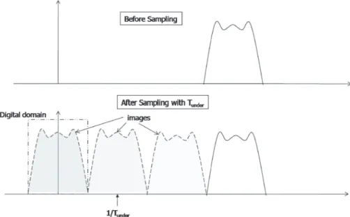
1.4.3 Undersampling
If a bandlimited non-baseband high-frequency signal is samples with a lower sample rate than the Nyquist rate, such as shown in Fig. 1.15, images signal will be generated at the lower frequency. In the figure, the high frequency bandlimited signal is sampled atfs = 1/Tunder which is 3 times lower than fN yquist. The non-baseband signal can be sampled with sampling frequency below Nyquist rate by using the undersampling technique [21]. The undersampling or bandpass sampling translates a high frequency bandpass signal to a near zero lowpass frequency such as shown in Fig. 1.16. The sampling frequency requirement is based on the signal bandwidth rather than its highest frequency. In the undersampling, the aliasing phenomenon is exploited to enable the ADC to sample the signal using a rate that intentionally aliases the high frequency signal into the operating range of the ADC.
Any out of band signal or noise must be kept to minimum because they will fold down to the desired signal band. A band pass filter (BPF) of very high Q is required to suppress the out of band signal. However, if the signal in the adjacent channel is
much larger than the desired signal, the BPF cannot eliminate the signal completely due to the restriction of the circuit size. The remaining adjacent channel signal will interfere the desired signal by folding down to the desired signal channel. As the result, the desired signal cannot be demodulated.
Jitter and phase noise of the sample clock signal can seriously degrade undersam- pling performance. This effect can reduce by using a high-quality crystal oscillator with simple, direct connections to the ADC. Some ADCs are specifically characterized for undersampling applications, while others are designed only for baseband sampling.
The system in Chapter 3 is implying undersampling.
Figure 1.16: Frequency conversion with undersampling.
1.4.4 Sample Rate Conversion
In SDR terminals, the problem of SRC emerges if the sample rate of the ADC is different from the symbol, chip, or bit rate of the processed signal. Since different communication standards are based on different master clock rates, it is mainly nec- essary to provide different clock rates. However, a tunable sample rate of ADC is a not a best choice because high complexity analog components must be avoided.
Since a signal processor should work at the minimum possible rate, SRC has to be implanted to a SDR receiver in order to process various kinds of radio standards [3].
The problem is because the baseband processing is usually carried out at the target rate and not at an arbitrary sample rate.
The most common structure for SRC is a combination of an L-factor upsampler, an anti-aliasing filter, and anM-factor downsampler, as illustrated in Fig. 1.17. This of SRC is called rational factor SRC.The SRC by L/M-ratio is done by upsampling the input data with L and then downsampling it by M [22, 23]. The upsampling by L factor is generated by inserting L−1 zeros between two consecutive samples of the input signal at the upsampler. The downsampling of the filtered upsampled signal is done by the downsampler by deleting all but every Mth sample of the signal. Although this technique is very useful for investigations, it is not applicable in practice in some systems due to the possibly very high intermediate sample rate and also required large effort for the anti-aliasing filter.
Implementation of fractional-SRC by using a cascaded-integrator comb (CIC) fil- ter can reduce the effort as the impulse response of the reconstruction filter can be realized by the comb filter [24]. However, this technique still requires the high in- termediate sample rate. Time-varying polyphase structure based fractional-SRC has been proposed to avoid the high intermediate frequency. The most commonly used implementation in this kind of structure is the Farrow structure which is a combi- nation of polynomial filtering and block processing [25, 26]. Polyphase realization for the CIC filter is also proposed in order to avoid the high intermediate sample rate [27]. However, the polyphase structure based fractional-SRC requires multiple of fractional delay filters and a lot of multiplexers which increase the complexity and power consumption.
Figure 1.17: Rational Factor SRC Direct Insertion/Cancellation SRC
A direct insertion/cancellation SRC has been proposed to realize high speed SRC with low complexity [28, 29]. This technique, which is also called non-interpolative resampling technique, does not interpolate the signal to the higher sample rate and avoid the high intermediate sample rate. This technique is suitable for application in the RF sampling receiver which samples data with a high OSR. In this technique, new samples are inserted to the data stream to increase the rate to a desired sample rate, or an amount of samples is deleted from a data stream to decrease the sample rate.
In the direct insertion scheme, α samples are inserted in every block ofN samples to increase the rate by (N+α)/N. The inserted samples can simply be zeros or a repeat of last value. In the direct cancellation scheme, α samples are deleted in every block of N samples to reduce the rate by (N −α)/N. This scheme can be realized with smaller chip size and lower power consumption as compared to the other techniques.
However this scheme suffers from large distortion as compared to the other technique.
Figure 1.18 shows the conventional periodic direct insertion/cancellation scheme.
The inserter/deleter block in the figure performs direct insertion/cancellation process.
The insertion or cancellation step is followed by filtering process by the anti-aliasing filter. The images that have been generated after insertion/cancellation process are removed by the anti-aliasing filter, before the signal is decimated to the desired sample rate.
In the direct insertion method, where αsample is inserted by repeating the R-th
sample in every N +α samples period to increase the data rate by (N +α)/N, the output signal is given by
y(kT2) = x
kN +R
N +α
T1
, (1.6)
wherex(k) in the k-th sample of the input sequence, T1 is the input sampling period, and T2 is the output sampling period. In the direct cancellation method, every R-th sample in every N samples period of the input signal sequence is deleted to reduce the data rate by (N −α)/N. The output signal is given by
y(kT2) =x
kN−R+ 1
N −α
T1
. (1.7)
The output of the inserter/deleter also produces images every 1/NT1 for a con- version rate of (N+ 1)/N and (N−1)/N, as illustrated in Fig. 1.19. The images are attenuated by using the anti-aliasing filter to avoid further distortion and aliasing.
The direct insertion/cancellation SRC scheme is discussed in Chapter 4.
Figure 1.18: Direct insertion/cancellation based fractional-SRC.
1.5 Adjacent Channel Interference
This thesis deals with ACI problems in SDR receiver system. ACI is interference caused by extraneous power from a signal in an adjacent channel. ACI may be caused by inadequate filtering, improper tuning, or poor frequency control, in either the
Figure 1.19: Generated images after direct insertion/cancellation.
reference channel or the interfering channel, or both. In the case of the SDR receiver, flexible receiver architecture with wideband signal receiving capability is required.
However, if the receiving bandwidth is wider, the received signal components may cause interference to each other. Higher requirements of filters, ADCs, and other analog components are needed to realize a wideband receiver. Moreover, some of the adjacent channel components may overlap directly to the desired channel. This research is focusing on signal processing methods to combat ACI problems and lower the requirements in The SDR receiver.
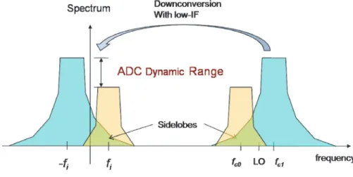
The performance of a wireless receiver is often determined by the signal-to-interference ratio (SIR), which is defined as the ratio of the data signal to the interference sig- nal. SIR is usually more critical to WLAN performance than the SNR. Interference resulting from signals which are adjacent in frequency to the desired signal is called ACI.
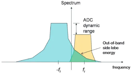
If the signal power in the adjacent channel is much larger than the desired signal, ADCs with very high dynamic range are required as shown in Fig. 1.20. This is not desirable as the large dynamic range leads to higher cost and power consumption of the ADCs.
Figure 1.20: Interference due to the signal in the adjacent channel.
1.5.1 Out-of-band Side-lobe Energy
The channels that are beside one another in the frequency domain may have some spectral overlap, causing impairment and interference. Although filtering is usually done to minimize interference from the adjacent channels, this interference also gen- erates side lobe energy that falls into the pass band of desired signal. If the adjacent channel is much larger than the desired signal, side band energy from the adjacent channel can dominate the channel’s noise floor, as illustrated in Fig. 1.20.
Figure 1.21 shows the usage of 4 channels in 100MHz band with 20 MHz interval that used in WLAN IEEE802.11a. The spectrum mask standard and spectrum of amplifier output of WLAN IEEE802.11a/g is shown in Fig. 1.22 [30]. The influence of ACI is determined by adjacent channel rejection level. The adjacent channel rejection level means, the limit of interference level compare to the desired signal level that allowed in the existence of interference from adjacent channel. For example, if the transfer rate is 24Mbps, the adjacent channel rejection is 8dB. Therefore, if the desired signal is -71dBm, it is possible to receive the desired signal even there is interference of -63dBm from adjacent channel.
The interference due to the out-of-band side-lobe energy in a WLAN system is dis- cussed in Chapter 2 and Chapter 3. An interference cancellation method to overcome the problem is also proposed in the chapters.
Figure 1.21: IEEE 802.11a channel spectrum.
1.5.2 ACI due to Undersampling
ACI problems also may occur when a high frequency signal is sampled at a lower sample rate as in undersampling technique. In the undersampling technique, any out of band signals or noise must be kept to a minimum because they will fold down into the output spectrum, exactly as illustrated in Fig. 1.23. In the figure, the adjacent channels are not sufficiently rejected, resulting interference from the downfolded adjacent channels. If the adjacent channel signal is significantly large, a high performance BPF with a very large Q is required to minimize the adjacent channel. Otherwise, the remaining components will aliased and translated to the desired band.
The effect of undersampling to a multi-channel reception system is discussed in
Figure 1.22: Spectrum mask standard and spectrum of amplifier output.
Chapter 3.
1.5.3 Aliasing due to Sample Rate Conversion
Image signal will be generated when the sample rate is upsampled, and the aliasing will happen when the signal is downsampled. If the adjacent channel is not com- pletely eliminated before the SRC process, aliasing from the adjacent channel may be overlapped on the desired signal.
As stated in 1.4.4, the direct insertion/cancellation SRC suffers from high dis- tortion and aliasing problems. Moreover, the images that generated by the adjacent channels may generated directly in the desired signal band, as illustrated in Fig. 1.24.
The interference cannot be rejected by anti-aliasing filter.
The effect of the aliasing due to the SRC scheme is discussed and a method to mitigate the effect is proposed in Chapter 4.
Figure 1.23: ACI due to the undersampling
Figure 1.24: ACI due to the direct insertion/cancellation SRC.
1.6 Motivation of the Research
1.6.1 Realization of SDR receiver
This dissertation discusses the signal processing in a SDR receiver system. The ideal concept for the SDR terminal is to attach an ADC directly to the antenna, as illustrated in Fig. 1.25 [1]. However, the ideal concept is not completely realizable due to the actual technology limits. The need of ultra high speed ADC cannot be realized by the current technology. The actual practical solution is to let the software processing stage be preceded by a front-end that preconditions the input signals to give them characteristics that enable the subsequent stage to elaborate them. The signal mixing based downconversion architecture such as superheterodyne receiver,
DCR, and low-IF receiver has been proposed for SDR.
A superheterodyne RF front-end architecture is adopted to lower the frequency of the received signals to IF values. A typical structure of the superheterodyne receiver architecture is shown if Fig. 1.26. After the first downconversion mixer, a passive off-chip channel select filter attenuates the out-of-channel signals to a sufficiently low level. A VGA, which follows the IF channel-select filter, decreases the dynamic range requirements of the ADC. Then, the desired signal is downconverted to the baseband before it is converted to a digital signal by an ADC. Although off-chip filters offer sufficient image rejection and selectivity, the input and output of each off-chip filter requires impedance matching that increases the power consumption in the RF front- end. The superheterodyne implementation of a multimode receiver requires multiple filters that not only increase the production cost but also the physical dimension of the handset. Thus, superheterodyne receiver is not a practical topology for multimode receiver designs.
DCR architecture, which has introduced the zero IF approach, supports efficient wireless terminal designs with a high level of integration [7, 10]. The structure of the DCR is shown in Fig. 1.27. In the DCR, the desired signal is downconverted directly to baseband signal with only single conversion stage. Thus, the DCR had lower complexity and power consumption. Low-IF receiver architecture has been proposed to avoid DC offset problem in a DCR. In the low-IF receiver, received signal is downconverted to a IF instead of downconvert it directly to a baseband signal. The IF is set to be relatively lower than that in the conventional IF receivers.
There are several merits by using low-IF receiver architecture. Low-IF receivers are not using SAW filter so that this architecture would have low cost and low power consumption as compared to super-heterodyne architecture. The low-IF receiver is much easier to make in one chip and the structure of the low-IF receiver can be much simpler than the super-heterodyne receiver.
Figure 1.25: Ideal SDR concept
The RF-sampling receiver scheme has been proposed recently to replace the con- ventional mixer-based downconversion scheme. The direct RF sampling technique is based on current sampling, which greatly simplifies the mixer circuit design [28]. In the RF-sampling architecture, the received signal is processed directly at the analog domain and sampled at the RF [12, 16]. Channel selection and demodulation are carried out in the digital domain. This architecture achieves the reduction of off- chip components and enables the realization of a single-chip receiver. RF-sampling receiver, which supports single chip and multi-mode designs, is a promising architec- ture for the next generation wireless terminals to realize a flexible wireless terminals with smaller physical dimensions. The structure of the RF-sampling architecture is shown in Fig. 1.29. The received signal is sampled at the same frequency of the carrier signal at the downconversion sampler to perform downconversion. This is followed by the decimation and filtering processes. The discrete signal is sampled at a high sample rate of the ADC. In the digital domain, digital signal processing and SRC are performed. Direct insertion/cancellation SRC is proposed to process the high sample rate signal.
In this dissertation, we use 2 approaches to realize the flexible receiver for SDR;
1. Low-IF signal mixing downconversion receiver architecture 2. RF sampling receiver architecture
In order to realize a SDR receiver, flexible receiver architecture with wideband
Figure 1.26: Superheterodyne receiver architecture.
Figure 1.27: DCR architecture.
signal receiving capability is required. However, if the receiving bandwidth is wider, the received signal components may interfere each other. In this study, the signal processing methods to combat the ACI problems in the SDR receivers are investigated and discussed.
In the first receiver architecture approach, the flexible wideband receiver is dis- cussed to be realized by utilizing the low-IF receiver with multi-channel reception capability. However, the multi-channel low-IF receiver suffers from a high interfer- ence from the adjacent channel. ADCs with a very high dynamic range are required to sample multiple of signals with a large power difference. Moreover, the out-of- band side lobe signal from the adjacent channel may be directly overlapped with the desired signal. The requirement of the high dynamic range ADC can be lowered by using complex BPF. Nevertheless, the problem of the analog BPFs is that it cannot eliminate the interference completely due to the restriction of the circuit size and
Figure 1.28: Low-IF receiver architecture.
Figure 1.29: RF-sampling receiver architecture.
the mismatch of the analog components. In Chapter 2, the ACI cancellation scheme with analog filter bank has been proposed to mitigate the influence from the adjacent channel.
ACI problems also may occur when a high frequency signal is sampled at a lower sample rate as in undersampling technique. In Chapter 3, undersampling technique is applied in this system in order to lower the required sampling frequency and power consumption. In order to realize the undersampling, all the out of band signal includ- ing noise and adjacent channel has to minimize as possible to avoid the overlapping with those signals. A high performance BPF with a very large Q is required to min- imize the out-of-band signals. In the chapter, the side effect of the undersampling technique to the multi-channel reception with low Q BPFs is investigated. An ACI
Figure 1.30: Motivation of the research.
cancellation scheme by using digital signal processing is proposed in the chapter to overcome the aliasing effect of the undersampling.
Images and aliasing which are appeared in an SRC process also bring the ACI problems as the aliasing from the adjacent channel may be overlapped on the desired signal. In the second receiver architecture approach, the ACI effects are small due to the usage of the high speed sample rate and high resolution of the ADC. However, the usage of the high speed fractional SRC introduces high aliasing to the converted signal. The image aliasing from the adjacent channel may directly be overlapped with the desired signal. Therefore, a new fractional SRC technique is investigated in Chapter 4, in order to overcome the aliasing and ACI problems and realize a high performance fractional SRC.
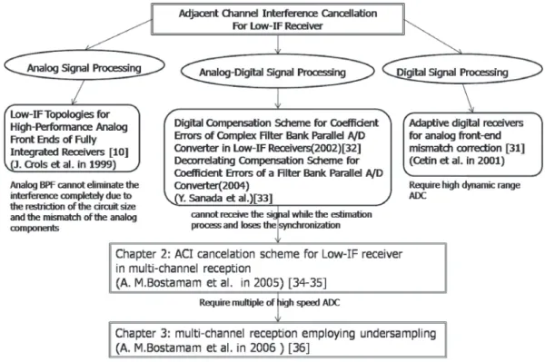
1.6.2 Adjacent Channel Interference Cancellation Scheme for Low-IF Receiver in Multi-Channel Reception
Chapter 2 discusses about a realization of high-speed handover for WLAN by using multi-channel reception concept. Chapter 2 proposes the method to solve the ACI
Figure 1.31: Relationship of the research about ACI cancellation in Low-IF receiver architectures.
problem due to the high dynamic range and out-of-band leakage from the adjacent channel. In the cases that the adjacent channel signal is much larger than the desired signal, high resolution ADCs have to be employed to accommodate such a signal with large dynamic range. The increase of the resolution of the ADC causes higher power consumption and higher implementation cost. Moreover the ACI component may directly overlap with the desired signal if the interference is much larger than desired signal.
The relationship of the research about ACI cancellation in Low-IF Receiver Ar- chitectures is shown in Fig. 1.31. In the previous studies, the ACI rejection or cancel- lation has been proposed by using analog circuits or digital signal processing. In [10], complex BPF, that can discriminate between the desired signal and the mirror signal, is proposed to be applied to the low-IF receiver. However, due to the restriction of the circuit size and the mismatch of the analog components, it is hard to realize high
Q analog filter. Several ACI cancellation technique using adaptive signal processing has been proposed [31]. However, the digital approach alone requires a very high dynamic range requirement of ADCs to be realized.
In order to reduce the required resolution of the ADCs and reduce the interference, an analog-digital signal processing technique has been investigated [32, 33]. This technique uses a BPF for each WLAN channel. The BPFs ease the dynamic range of the ADCs and makes the modulation of multi-channel possible. Nevertheless, the problem of the analog BPFs is that it cannot eliminate the interference completely due to the restriction of the circuit size and the mismatch of the analog components.
Thus, combination of the analog and digital signal processing is indispensable. The problem of this scheme is that it requires estimating the characteristics of the analog filters. This system requires the signal generator in the receiver to generate known waveform for the estimation. While estimating the characteristics, the receiver can not receive the signal and loses the synchronization.
In this chapter, a new ACI cancellation scheme with the analog filter bank has been proposed [34, 35]. The proposed scheme automatically estimates the characteristics of the interference signal and cancels it from the received signal through Wiener filter. The proposed scheme can estimate the characteristics of the interference signal while it maintains the synchronization to the received signal even though the training sequence is required periodically. The results obtained from experiment show that the proposed technique enables multi-channel reception and work with the low resolution ADCs.
1.6.3 Undersampling for Adjacent Channel Interference Can- cellation Scheme
The objective of Chapter 3 is to lower the requirements of ADCs in the scheme that is proposed in Chapter 2 [35]. The proposed scheme in Chapter 2 requires
multiple of high speed ADCs to prepare the filter bank. Also the low-IF receiver requires higher sampling frequency than the conventional architecture such as super- heterodyne. Thus, the ADCs in the low-IF receiver require higher power consumption than the conventional scheme.
Undersampling technique is employed in this scheme in order to lower the required sampling frequency and power consumption of the ADC [36]. In the conventional sampling technique, Nyquist rate is required to sample the received signal. Desired signal can be sampled with sampling frequency below Nyquist rate by using the undersampling technique. The undersampling translates a high frequency bandpass signal to a near zero lowpass frequency. The sampling frequency requirement is based on the signal bandwidth rather than its highest frequency. Sampling at reduced rates eases many of the ADC requirements, and decreases power consumption, thus increasing battery lifetime, and the overall receiver size. The need for very high performance programmable devices is also reduced.
Any out of band signal or noise must be kept to minimum because they will fold down to the desired signal band. A BPF of very high Q is required to suppress the out of band signal. If the signal in the adjacent channel is much larger than the desired signal, the BPF cannot eliminate the signal completely due to the restriction of the circuit size. The remaining adjacent channel signal will interfere the desired signal by folding down to the desired signal channel. As the result, the desired signal cannot be demodulated. In Chapter 3, the side effect of the undersampling technique to the multi-channel reception is investigated through the experiment. The influence of aliasing effect in the undersampling is compensated in digital domain by using the adaptive digital signal processing.
1.6.4 Fractional Sample Rate Conversion for SDR
Since different communication standards are based on different master clock rates, it is mainly necessary to provide different clock rates. Since a signal processor should work at the minimum possible rate, SRC has to be implanted to a SDR/CR receiver in order to process various kinds of radio standards [3].
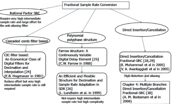
The relationship of the research about Fractional SRC is shown in Fig. 1.32. The most common structure for fractional SRC is a combination of anL-factor upsampler, an anti-aliasing filter, and an M-factor downsampler. The SRC by L/M-ratio is done by upsampling the input data with L and then downsampling it byM [23, 27].
However, this technique is not applicable in practice in some systems due to the possibly very high intermediate sample rate and also required large effort for the anti- aliasing filter. Implementation of fractional-SRC by using a CIC filter can reduce the effort as the impulse response of the reconstruction filter can be realized by the comb filter [23, 24]. However, this technique still requires the high intermediate sample rate. Time-varying polyphase structure based fractional-SRC has been proposed to avoid the high intermediate frequency. The most commonly used implementation in this kind of structure is the Farrow structure which is a combination of polynomial filtering and block processing [23, 25–27]. Polyphase realization for the CIC filter is also proposed in order to avoid the high intermediate sample rate [37]. However, the polyphase structure based fractional-SRC requires multiple of fractional delay filters and a lot of multiplexers which increase the complexity and power consumption.
Chapter 4 proposes a new fractional SRC scheme based on a direct insertion/cancellation scheme. This technique is also called non-interpolative resampling technique [28, 29].
This scheme is suitable for signals that are sampled at a high sample rate and con- verted to a lower sample rate. The objective of the scheme is to realize a high-speed and high-performance SRC scheme with low-complexity and lower power consump-
Figure 1.32: Relationship of the research on fractional SRC.
tion. High-speed SRC scheme for high sample rate data can be realize by a direct insertion/cancellation scheme. This technique is suitable for application in the RF sampling receiver which samples data with a high OSR.
However, the direct insertion/cancellation technique suffers from large aliasing and distortion as compared to the other SRC techniques [29]. The aliasing from an adjacent channel interferes the desired signal and degrades the performance. There- fore, a modified direct insertion/cancellation scheme is proposed in order to realize high performance resampling. The distortion noise or aliasing can be reduced by applying multiple sets of inserters/deleters [38, 39]. This technique reduces the re- quired complexity of an anti-aliasing filter structure, and improves the performance of a direct insertion/cancellation based SRC system.
Chapter 2
Adjacent Channel Interference Cancellation Scheme for Low-IF Receiver in Multi-Channel
Reception
In this chapter a new adjacent channel interference (ACI) cancellation scheme for multi-channel signal reception with low-IF receivers is investigated through the ex- periment. In the low-IF receivers, the signal in the mirror frequency causes interfer- ence to the desired signal. In the proposed analog-digital signal processing scheme, channel selection is made by analog complex band pass filter and the signal is re- construct by Wiener filter to eliminate the interference effect in order to improve the performance. This Chapter also describes an application of multi-channel reception for quick roaming in WLANs system.
2.1 Introduction
Access points for wireless LANs have been installed in many places such as airports or hotels. Though the roaming capability has been specified in the IEEE802.11 standard, it is not able to handle a quick roaming for Voice over Internet Protocol (VoIP) applications. Therefore, multi-channel reception is required for VoIP over WLAN.
One of the receiver architecture applicable for such applications is the low-IF receiver [2, 10]. In the low-IF receiver, the IF is set to be relatively lower than that in conventional IF receivers. The low-IF receiver are not using SAW filter so that this architecture would have low cost and low power consumption compared to conventional super-heterodyne architecture. The IF signal is sampled and converted to the digital signal with analog-digital converters (ADCs). The final process of down conversion is carried out in the digital domain. This architecture is applicable for multi-channel reception as the choice of the channel can be done with digital signal processing. However, in some cases the next access point may be far away from the current one and the dynamic range between the signals from the current access point and those from the next one may be quite large. This means that high resolution ADCs have to be employed to accommodate such a signal with large dynamic range.
The increase of the resolution of the ADC causes higher power consumption and higher implementation cost. Moreover, the ACI component may directly overlap with the desired signal if the interference is much larger than desired signal.
In order to reduce the required resolution of the ADCs and reduce the interfer- ence, an analog-digital signal processing technique has been investigated [32,33]. This technique uses a band pass filter (BPF) for each WLAN channel. The BPFs ease the dynamic range of the ADCs and makes the modulation of multi-channel possible.
Nevertheless, the problem of the analog BPFs is that it cannot eliminate the inter- ference completely due to the restriction of the circuit size and the mismatch of the analog components. Thus, combination of the analog and digital signal processing is indispensable. The problem of this scheme is that it requires estimating the charac- teristics of the analog filters. This system requires the signal generator in the receiver to generate known waveform for the estimation. While estimating the characteristics, the receiver can not receive the signal and loses the synchronization.
In this chapter, a new ACI cancellation scheme with the analog filter bank has
been proposed. The proposed scheme automatically estimates the characteristics of the interference signal and cancels it from received signal through Wiener filter. The proposed scheme can estimate the characteristics of the interference signal while it maintains the synchronization to the received signal through training sequence is required periodically. The results obtained from experiment show that the proposed technique enables multi-channel reception and work with the low resolution ADCs.
2.2 Multi-Channel Reception
2.2.1 Roaming Protocol
Figure 2.1: Roaming example with IEEE802.11 MAC Protocol.
The mobility of WLAN terminals among multiple base stations is specified in Ex- tended Service Set (ESS) of IEEE802.11 MAC protocol [40]. An example of roaming capability with IEEE802.11 MAC is shown in Fig. 2.1. A handover occurs when a terminal moves beyond the radio coverage of an access point (AP), and enters cover-