5MHz PWM-Controlled Current-Mode
Resonant DC-DC Step-Down Converter Using GaN-HEMTs Akinori Hariya
Student Member, IEEE Nagasaki University 1-14 Bunkyo-machi, Nagasaki-shi, Nagasaki, Japan [email protected]
Satoshi Tomioka
TDK-Lambda Corporation 2704-1 Settaya-machi, Nagaoka-shi, Nigata, Japan [email protected]
Ken Matsuura
TDK Corporation 2-15-7 Higashiowada, Ichikawa-shi, Chiba, Japan [email protected]
Yoichi Ishizuka
Member, IEEE Nagasaki University 1-14 Bunkyo-machi Nagasaki-shi, Nagasaki, Japan
Hiroshige Yanagi
TDK-Lambda Corporation 2704-1 Settaya-machi, Nagaoka-shi, Nigata, Japan [email protected]
Tamotsu Ninomiya
Fellow, IEEE
The International Centre for the Study of East Asian Development 1-8 Hibikino, Wakamatsu-ku Kitakyushu-shi, Fukuoka, Japan
Abstract -- High power efficiency and high power density are required in regulated isolated DC-DC converters. In this paper, a novel pulse width modulation (PWM) control method which is suitable for the isolated current-mode resonant DC-DC converter operated at MHz level switching frequency is proposed. The output voltage with the proposed method can be regulated with no additional components at fixed switching frequency. In addition, zero voltage switching (ZVS) of primary- side switches at turn-on can be maintained. The principle of the proposed method and the method of ZVS operation in the proposed method are explained.
Some experiments have been performed with a 5MHz isolated step-down DC-DC converter using Gallium Nitride High Electron Mobility Transistors (GaN-HEMTs); the output voltage is 12V and the total volume of the circuit is 16.14cm3. With the proposed PWM control method, input voltage range is 42-45.5V, and maximum load current range is 10A at Vi = 45.5V.
The ZVS of the primary-side switches at turn-on is confirmed in all experimental regions, and the maximum power efficiency is 89.2%.
Index Terms— DC-DC power converters, Gallium nitride, Pulse width modulation converters, Switching converters, Zero voltage switching.
I. INTRODUCTION
Recently, high power efficiency and high power density power conversion systems have been required in information and communication technology (ICT) equipment due to increases in system power consumption. Therefore, intermediate bus architectures (IBAs) have been introduced in this field in recent years [1]. The performances of three basic IBAs are investigated in [2]. The literature reported that the double regulated IBA has the potential of the best performance. This architecture is composed of a regulated bus converter and regulated point of load (POL) converters. An isolated step-down DC-DC converter is used as the bus converter in IBA. The rated input voltage is 48V, and the
output target voltage is 12V which is the intermediate bus voltage. At the next stage of bus conversion, 12V is regulated in POLs to e.g. 2.5 or 1.0V required by each load. In this architecture, the design of the regulated bus converter is especially difficult due to requirements both of isolation and regulation. Thus, research of regulated bus converters is important for more improvement of the double regulated IBA.
In this paper, a 5MHz PWM-controlled current-mode resonant DC-DC step-down converter for regulated bus converters is discussed.
Corresponding to the requirement of high power density, the increase in the switching frequency of these converters has been considered to be one of the key approaches.
Therefore, a 5MHz switching frequency, which is relatively high for isolated DC-DC converters, is adopted in this research [3]-[5]. However, by adopting a high switching frequency, power loss such as switching loss and gate driving loss increases. To solve this problem, the current-mode resonant DC-DC converter is used because this converter can reduce switching loss. Also, GaN-HEMTs are suitable for high switching frequency operation as semiconductor switches because of low gate driving loss.
The output voltages of current-mode resonant DC-DC converters are usually controlled by pulse frequency modulation (PFM). However, PFM controlled current-mode resonant DC-DC converter are not suitable for miniaturization.
The details are described in section III.
The novel PWM control method which is suitable for the isolated current-mode resonant DC-DC converter operated at MHz level switching frequency is proposed. This converter topology is the same as the conventional current-mode resonant DC-DC converter with synchronous rectification. In general, when load current increases or input voltage decreases from rated input voltage, the output voltage is decreased. Therefore, to maintain constant output voltage, boost conversion is needed. The proposed PWM control method can regulate output voltage without any additional
components. By using the transformer’s leakage inductance and secondary-side synchronously rectifying switches, secondary-side boost conversion operation can be realized. In MHz level switching operation for high power density, switching loss increases dramatically. To suppress switching loss, ZVS operation is needed. The proposed PWM control method can maintain ZVS of primary-side switches at the turn-on in all operating regions.
The targets of the research are to obtain the high performances which are small volume, 42-53V input voltage range, which is used in information servers and other computer applications [6], 10A of maximum load current range, and the realization of ZVS of primary-side switches at turn-on.
In section II, the approach of the realization of DC-DC converter operated at MHz level switching frequency is described. In section III, the issue of the conventional PFM- controlled current-mode resonant DC-DC converter is revealed. In section IV, the proposed PWM-controlled current-mode resonant DC-DC converter is explained. In section V, the experimental results are demonstrated.
II. THEAPPROACHOFTHEREALIZATIONOFDC-DC CONVERTEROPERATEDATMHZLEVELSWITCHING
FREQUENCY
For miniaturization of the DC-DC converter, the increase in the switching frequency is considered to be one of the key approaches.
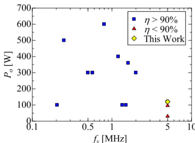
As shown in Fig. 1, there are not many reports in the literature for the region of over 5MHz switching frequency and 100W output power with more than 90% of power efficiency. Therefore, this research challenges 5MHz of switching frequency at 120W of output power. To suppress increasing core power loss with high switching frequency, NiZn ferrite core is used [18]. To increase power density, a multilayer printed circuit board (PCB) is employed in this research. The details of PCB layout technique is shown in [4].
Also, to increase more power density, a planar transformer is employed in the research. The planar transformer is directly manufactured with multi-layered pattern in the PCB.
In the prototype circuit, conventional hard-switched gate driving is used for the GaN-HEMTs. Therefore, the gate driving loss Pd is expressed by
s GS G
d Q V f
P (1) where QG is gate charge, VGS is gate-to-source voltage of GaN-HEMT, and fs is switching frequency. From eq. (1), this power loss is proportional to fs.
For reducing gate driving loss, GaN-HEMTs are adopted in this research because GaN-HEMTs have low QG and be driven at low gate-to-source voltage. The benefits of GaN- HEMTs are not purely low Qg, but a physically smaller transistor for a given low drain-to-source on resistance Rds(on)
and Vgs blocking capability. Due to physically smaller device with lower parasitic capacitances, faster device switching speed results. Additionally, GaN-HEMTs have no source-to- drain recovery charge [19] and low package inductance
because of small package size [20]. Other researches have validated the effectiveness of GaN-HEMTs for high switching frequency DC-DC converters [7]-[10], [14]. Also, GaN- HEMTs have been proved more effective than silicon devices in [7], [9]-[11], [13].
However, because of GaN-HEMTs having low gate-to- source threshold voltage Vth, low maximum gate-to-source voltage VGSS, and high source-to-drain voltage VSD, it is difficult to drive GaN-HEMTs. Therefore, suitable drive circuit for GaN-HEMTs is needed. Some literatures show that driver LM5113 is suitable for driving GaN-HEMTs [21].
By adopting a high switching frequency, switching loss increases dramatically. However, if switches can achieve soft- switching such as ZVS operation at the turn-on, the switching loss can be suppressed to almost zero. In this research, current-mode resonant DC-DC converter topology featuring ZVS of primary-side switches at turn-on is adopted. Many studies of this circuit topology in MHz level switching operation have been done [7], [10], [14].
III. THEISSUEOFTHECONVENTIONALPFM- CONTROLLEDCURRENT-MODERESONANTDC-DC
CONVERTER
To reduce the volume of the DC-DC converter, the resonant inductance of the converter needs to be minimized.
For effective miniaturization of the converter, the miniaturization of resonant inductance is important.
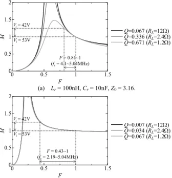
Meanwhile, to reduce the switching loss, the current-mode resonant DC-DC converter is widely used [7], [10], [12]-[17], [22], [23]. Generally, the current-mode resonant DC-DC converter is controlled by PFM control which varies switching frequency. In Fig. 2, the relation of resonant inductance and frequency variance is shown. Lr =100nH and Lr = 10nH are in Fig. 2 (a) and (b), respectively. The other parameters are Vi = 48V, n = 2.2, Lm = 200nH.
In this figure, the definitions of the converter parameters are M
2nVo
Vi , (2)0.1 0.5 1 5 10
0 100 200 300 400 500 600 700
> 90%
< 90%
This Work
fs [MHz]
Po [W]
Fig. 1. The performances of isolated DC-DC converters which have 48V of input voltage and 12V of output voltage in the previous papers
presented at APEC from 2014 to 2010 and ECCE from 2013 to 2009 [4], [5], [7]-[17].
r
m L
L
, (3) f0
f
F s , (4)
LrCr
f0 1 2 , (5)
0 0 2f
, (6) Rac
Z
Q 0 , (7)
8 2
2 L
ac n R
R (8)
and
r r C L
Z0 (9) where turn ratio n, magnetizing inductance Lm, resonant inductance Lr, switching frequency fs, resonant capacitance Cr
and load resistance RL. According to [22], eq. (2) can be converted from eqs. (3) to (8) as (10). Eq. (10) can be
2 2 2 2
1 1 1
1 1
1
F F F Q
M (10)
It is assumed that input voltage range is from 42 to 53V at RL = 1.2 and Vo = 12V. The influence of Lr on M can be confirmed from Fig. 2 (a) and (b). In case of Lr = 100nH, for realization of the range, F is changed from 0.81 to 1. In contrast, in case of Lr = 10nH, for realization of the range, F is changed from 0.43 to 1.
If large resonant inductance value is used, the region of switching frequency is narrow, which leads to small size noise filter. However, to obtain large resonant inductance value, the physical size of the inductor becomes large. If small resonant inductance value is used, the region of switching frequency is wide, which leads to large size noise filter. There is a trade- off between the size of the required noise filter and resonant inductor.
As the result, for the miniaturization of the DC-DC converter, it is shown that pure PFM control is not appropriate. Therefore, PWM-controlled current-mode resonant DC-DC conversion has been proposed [3], [5].
IV. THEPROPOSEDPWM-CONTROLLEDCURRENT- MODERESONANTDC-DCCONVERTER In the previous researches, some PWM-controlled current- mode resonant DC-DC converters have been presented [24]- [26]. For example, the method of additional auxiliary circuits for regulating output voltage [24], [25], and the method of controlling the duty ratio of primary-side switches [26] have been proposed. However, these methods need some additional components for regulating output voltage. On the other hand, the output voltage of the proposed current-mode resonant DC-DC converter can be controlled without any additional components at fixed switching frequency. In addition, ZVS of primary-side switches at turn-on can be accomplished in the proposed method. In this section, the principle of the proposed method and the method for achieving ZVS turn-on are explained.
A. The Circuit Topology
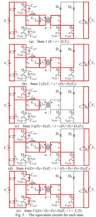
The circuit topology is based on a half-bridge type current- mode resonant DC-DC converter as shown in Fig. 3. The primary-side is the half-bridge topology. Q1 and Q2 are driven in 50% duty ratio, alternatively. Cr1 and Cr2 are the resonant capacitors which have the same capacitance and also make averaged voltage of vc to one half of the input. The inside of the broken line is the equivalent circuit of the magnetic transformer, where Lr is leakage inductance, and Lm is the transformer’s magnetizing inductance. The turn ratio is n : 1.
Lr is used as the resonant inductance. The secondary-side is the full-bridge topology composed with diodes D1 and D2 for high-side arm switches, and transistors Q3 and Q4 for low-side arm switches.
B. The Principle of the Proposed PWM Control Method To simplify analysis of the circuit operation, the following assumptions are made:
GaN-HEMTs are treated as ideal switches;
The reverse-conduction voltage drops of the primary- side switches are neglected;
F= 0.81~1 (fs= 4.1~5.04MHz) Vi= 53V
Vi= 42V
0 0.5 1 1.5
0 0.5 1 1.5
Q=0.067 (RL=12) Q=0.336 (RL=2.4) Q=0.671 (RL=1.2)
F
M
(a) Lr = 100nH, Cr = 10nF, Z0 = 3.16.
0 0.5 1 1.5
0 0.5 1 1.5 2
Q=0.007 (RL=12) Q=0.034 (RL=2.4) Q=0.067 (RL=1.2)
F
M
F= 0.43~1 (fs= 2.19~5.04MHz) Vi= 53V
Vi= 42V
(b) Lr = 10nH, Cr = 100nF, Z0 = 0.316.
Fig. 2. The static characteristics of LLC resonant DC-DC converter with the conventional PFM control method.
Vi LrLm n : 1 Cr1
Cr2
Vo
RL
Co
Q1
Q2
D1
D2
Q3 Q4
Transformer
Fig. 3. The circuit topology used in this paper.
Because of the gate is shorted to the source by the gate drivers during off-term, drain-to-gate capacitance therefore appear in parallel with drain-to-source capacitance of each GaN-HEMTs. Therefore, the capacitances of the primary-side GaN-HEMTs which labeled Coss1 and Coss2 are defined as the sum of the drain-to-gate capacitance and the drain-to-source capacitance during off-term, respectively. These capacitances are assumed as Coss1Coss2 and
2
1 oss
oss
oss C C
C ;
Resonant capacitances are satisfied Cr1Cr2 ,
2
1 r
r
r C C
C ;
The forward voltage drops and the parasitic capacitances
of the secondary-side diodes are neglected;
The output capacitances and the reverse-conduction voltage drops of the secondary-side switches are neglected;
The output voltage is constant;
The output voltage can be controlled by changing the duty ratio of Q3 and Q4, simultaneously. When the duty ratio is less than 0.5, the circuit operates as well as conventional current resonance circuit. When the duty ratio is more than 0.5, the circuit operates in the proposed operation.
The operational waveforms are shown in Fig. 4. The circuit operation is separated into 10 states in the proposed method. First half switching cycle is from state 1 to 5. Second half switching cycle is the remaining states. The second half switching cycle is symmetrical in operation to the first half
Vi LrLm
n : 1 Cr1
Cr2
Vo RL
Co Q1
Q2
D1
Coss1
Coss2
D2
Q3 Q4
vc ir
im vDS
vp
vs
vGS2
vGS1
vGS3 vGS4 (a) State 1 (0 < t < D1Ts).
Vi LrLm
n : 1 Cr1
Cr2
Vo
RL
Co Q1
Q2
D1
Coss1
Coss2
D2
Q3 Q4
vc ir
im vDS
vp
vs
vGS2
vGS1
vGS3 vGS4 (b) State 2 (D1Ts < t < (D1+D2)Ts).
Vi LrLm
n : 1 Cr1
Cr2
Vo RL
Co Q1
Q2
D1
Coss1
Coss2
D2
Q3 Q4
vc ir
im vDS
vp
vs
vGS2
vGS1
vGS3 vGS4 (c) State 3 ((D1+D2)Ts < t < (D1+D2+D3)Ts).
Vi
LrLm
n : 1 Cr1
Cr2
Vo RL Co Q1
Q2
D1
Coss1
Coss2
D2
Q3 Q4
vc ir
im vDS
vp
vs
vGS2
vGS1
vGS3 vGS4
(d) State 4 ((D1+D2+D3)Ts < t < (D1+D2+D3+D4)Ts).
Vi LrLm
n : 1 Cr1
Cr2
Vo
RL
Co Q1
Q2
D1
Coss1
Coss2
D2
Q3 Q4
vc ir
im vDS
vp
vs
vGS2
vGS1
vGS3 vGS4 (e) State 5 ((D1+D2+D3+D4)Ts < t < Ts/2).
Fig. 5. The equivalent circuits for each state of the proposed PWM method.
Fig. 4. The operational waveforms of the proposed PWM control.
TABLE I. CIRCUIT OPERATION STATES
State FET Diode
Q1 Q2 Q3 Q4 D1 D2
State 1 ON OFF ON ON OFF OFF
State 2 ON OFF ON OFF OFF ON
State 3 ON OFF ON OFF OFF OFF
State 4 ON OFF ON ON OFF OFF
State 5 OFF OFF ON ON OFF OFF
switching cycle. Therefore, because same analytical results can be obtained in each switching cycle, the description for the second half switching cycle is omitted. The switch combination is shown in TABLE I. The equivalent circuits for each state of a half switching term are shown in Fig. 5. In this figure, the switches drawn with weak colors represent OFF, and red line represents current flow.
The definitions of the duty ratio D are followed as
s on T T
D , (11)
5 4
2 1
1 D D D
D , (12) 2
5 1
4 3 2
1D D D D
D (13)
and
) operation
proposed (
5 . 0
) operation al
convention (
5 . 0
D
D (14)
where Ts is the switching period, and Ton is the on-term of Q3 and Q4. D1~D5 are the duty ratio of each state. The definitions of the resonant operation are as follows;
LrLm
Cr
1 1 , (15)
Lr Lm
CrZ1 (16) and
oss r oss1 LC
(17)
The definitions of the initial value of the variables are as follows;
i cc V V
v10 2 (18) and ir1
0 Ir (19) The descriptions for each state are described below.State 1 (0 < t < D1Ts):
In this state, t1 is defined as t1 = t. The primary-side switch Q1 is turned ON. Also, the secondary-side switches both Q3
and Q4 are turned ON. Q3 and Q4 are overlapped as indicated with the light gray area in Fig. 4. The resonant inductance Lr
is magnetized by ir for boosting output voltage. From the figure, vc1 (t1) and ir1 (t1) become
1
01
0
01
1t V V 2 V cos t Z I sin t
vc i i c r (20)
and ir1
t1 1Z0
Vi 2Vc
sin0t1 Ircos
0t1 . (21) The final values of the state 1 are
s
c
c v DT
V2 1 1 (22) and Ir2ir1
D1Ts
. (23) State 2 (D1Ts < t < (D1+D2)Ts):In this state, t2 is defined as t2 = t-D1Ts. After Q4 is turned OFF, the direction of the voltage applied to D2 is inverted, and diode of D2 becomes ON. The inductance current which is magnetized in state 1 flow through diode D2 and switch Q3, to the load. From the figure, vc2 (t2) and ir2 (t2) become
2V
22 V nV
cos 0t2
Z0I 2sin
0t2
nV V t v
r o
i c
o i c
(24)
and
0 2
2
2 0 2
0 2 2
cos
sin 1
t I
t nV
V V Z t i
r
o i c r
. (25)
The final values of the state 2 are
s
c
c v D T
V3 2 2 (26) and Ir3ir2
D2Ts
. (27) State 3 ((D1+D2)Ts < t < (D1+D2+D3)Ts):In this state, t3 is defined as t3 = t-D1Ts-D2Ts. The direction of the diode D2 current is inverted, and diode of D2 becomes OFF. In the state, resonant current ir equal to magnetizing current im. From the figure, vc3 (t3) and ir3 (t3) become
3
3
13
1 3
13
3t V V V cos t Z I sin t
vc i c i r (28)
and ir3
t3 1Z1
Vc3Vi
sin1t3 Ir3cos
1t3 . (29) The final values of the state 3 are
s
c
c v DT
V4 3 3 (30) and Ir4ir3
D3Ts
. (31) State 4 ((D1+D2+D3)Ts < t < (D1+D2+D3+D4)Ts):In this state, t4 is defined as t4 = t-D1Ts-D2Ts-D3Ts. This state is similar to state 1. In the state, the resonant inductance Lr is magnetized by ir for ZVS of the primary-side switch at turn-on. Q3 and Q4 are overlapped as indicated with the dark gray area in Fig. 4. From the figure, vc4 (t4) and ir4 (t4) become
4
4
04
0 4
04
4t V V V cos t Z I sin t
vc i c i r (32)
and ir4
t4 1Z0
Vc4Vi
sin0t4
Ir4cos
0t4
. (33) The final values of the state 4 are
s
c
c v D T
V5 4 4 (34) and Ir5ir4
D4Ts
. (35) State 5 ((D1+D2+D3+D4)Ts < t < Ts/2):In this state, t5 is defined as t5 = t-D1Ts-D2Ts-D3Ts-D4Ts. The primary-side switch Q1 is turned OFF. All primary-side switches are turned OFF, called dead time. The parasitic capacitor Coss1 of Q1 is discharged by a half of resonant inductance current ir. Q3 and Q4 are overlapped as indicated with the dark gray area in Fig. 4. From the figure, vc5 (t5), vDS5
(t5) and ir5 (t5) become
2 5 02
2 02
5
2 5 02
2 02
2 5 0
2 02
2 5 5 0 5 5
sin cos
t C
I V t V
V V V
t v
oss oss
r r
oss oss
i c
oss i c c
c
, (36)
2 5 02
2 02
5
2 5 02
2 02
2 5
2 02
2 5 5
5
sin cos
t C
I V t V
V V t V
v
oss oss
oss r
oss oss
i c oss
i oss
i c DS oss
(37)
and
2 5 02
5
2 5 02
2 02
5 5 5
cos
sin
t I
t L
V t V
i
oss r
oss oss
r
i r c
. (38)
C. The Method for Achieving ZVS of Primary-side Switches at Turn-On in the Proposed PWM Control
To accomplish ZVS of the primary-side switches at turn-on, small magnetizing inductances Lm have been used in current- mode resonant DC-DC converters generally. However, small Lm value leads to increase of primary-side current which can cause a reduction of power efficiency. Therefore, to accomplish ZVS operation in the proposed method, phase- shift between primary and secondary-side switches which controls resonant current is proposed.
As shown in Fig. 4, the proposed operation has phase-shift between primary and secondary-side switches. tps is the time length of the phase-shift. Without the phase-shift, tps = 0ns, the previous state of the dead time becomes discontinuous current state. With this situation, initial current cannot be charged enough for ZVS operation because of secondary-side parasitic capacitances. Therefore, even with the long dead time duration, ZVS cannot be achieved. With the phase-shift, the problem of the initial current can be solved. From eqs.
(33) and (35), the initial current of the dead time, Ir5 is
c i
s
r
s
r Z V V D T I D T
I 51 0 4 sin0 4 4cos 0 4 . (39) The term of the phase-shift becomes
s s
ps DT DT
t 4 5
. (40)
In eq. (40), as defined as the D5Ts is fixed, the term of state 4 becomes larger with the increase of tps. Ir5 is related to tps
almost linearly. As Ir5 increases, the amount of electrical charge qr5 which flows in the resonant inductance during dead time becomes larger.
Meanwhile, the output capacitances of GaN-HEMTs are not constant. The value of output capacitance depends on drain-to-source voltage. The influence of drain-to-source voltage on output capacitance is confirmed in [19], as shown in Fig. 6. In considerations of this influence, the initial electrical charge of dead time qoss is expressed by
Vi oss DS DS
oss C v dv
q 0 (41)
From eq. (41), the influence of drain-to-source voltage on qoss
can be obtained, as shown in Fig. 6.
For an example, when input voltage is 42V, qoss1 and qoss2
0 10 20 30 40 50
0.6 0.8 1 1.2 1.4
0 10 20 30
vDS [V]
Coss1, Coss2 [nF] qoss1, qoss2 [nC]
Coss1, Coss2
qoss1, qoss2
42V
31.2nC
Fig. 6. The influence of vDS on Coss1, Coss2 and qoss1, qoss2.
Fig. 7. The effect of the phase-shift tps on | qr5 |.
0.5 0.55 0.6 0.65
0 0.5 1 1.5 2
RL=12
RL=2.4
RL=1.2
D
M
D= 0.5~0.605 Vi= 53V
Vi= 42V
(a) Lr = 100nH, Cr = 10nF, Z0 = 3.16.
0.5 0.55 0.6 0.65
0 0.5 1 1.5 2
RL=12
RL=2.4
RL=1.2
D
M
D= 0.5~0.55 Vi= 53V Vi= 42V
(b) Lr = 10nH, Cr = 100nF, Z0 = 0.316.
Fig. 8. The static characteristics of resonant DC-DC converter with the proposed PWM control method.
are 32.1nC from Fig. 6. Therefore, equivalent output capacitances Coss1 and Coss2 are 764pF, respectively. In the conditions of Coss = 1528pF, Vi = 42V, RL = 2ohm, D5Ts = 10ns, the relation of tps and qr5 are shown in Fig. 7. The electrical charge qr5 can be calculated with
DTs r
r i t dt
q 5
0 5
5 (42)
For achieving ZVS, qr5 has to be larger than the amount of the electrical charge of the output capacitance of the switches as
oss
r q
q5 (43) In this case, due to qoss = 64.2nC, if qr5 is larger than 64.2nC, ZVS operation can be achieved. From the figure, it can be seen that the phase-shift tps between primary and secondary- side switches are valid for ZVS operation in the proposed PWM control.
D. The Static Characteristics of the Proposed Method at MHz Level Operation
Similar to section III, two examples of the static characteristics of the proposed PWM controlled current-mode resonant DC-DC converter are shown in Fig. 8. Lr =100nH and Lr = 10nH are in Fig. 2 (a) and (b), respectively. The other parameters are Vi = 48V, n = 2.2, Lm = 200nH.
It is assumed that input voltage range is from 42 to 53V at RL = 1.2 and Vo = 12V. In case of Lr = 100nH, for realization of the range, D is changed from 0.5 to 0.605. In contrast, in case of Lr = 10nH, for realization of the range, D is changed from 0.5 to 0.55. By comparing between two parameters, the case of Lr = 10nH can control in narrow duty ratio than the other one. Therefore, the proposed PWM control method is seen to be suitable for the miniaturization of the DC-DC converter because the output voltage can be controlled with small resonant inductance.
V. EXPERIMENTALRESULTS
In this section, it can be confirmed the difference between the experimental results of the proposed method and the targets of the research.
A. The Experimental Conditions
As a prototype digital controller, a field programmable gate array (FPGA) Cyclone IV is used, which generates individual gate signal for each switch. The on-terms of the gate signals are manually changed with software. The resolution of the gate signals is 1nano second.
Some experiments have been performed with parameters as shown in TABLE II. Components used in the experiment are shown in TABLE III.
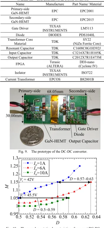
The prototype 5MHz isolated DC-DC converter with GaN- HEMTs is shown in Fig. 9. The total volume of the prototype circuit is 16.14cm3.
TABLE II. EXPERIMENTAL PARAMETERS
Specifications Value
Input voltage: Vi 48V
Transformer ratio n : 1 2 : 1
Switching frequency: fs 5MHz
Transformer leakage inductance: Lr 37nH Transformer magnetizing inductance: Lm 200nH
Resonant capacitor: Cr1,Cr2 15.5nF
Output capacitor: Co 18.8F
TABLE III. EXPERIMENTAL COMPONENTS Name Manufacture Part Name/ Material Primary-side
GaN-HEMT EPC EPC2001
Secondary-side
GaN-HEMT EPC EPC2015
Gate Driver TEXAS
INSTRUMENTS LM5113
Diode DIODES PDS1040L
Transformer Core
Material TDK SY22
(NiZn Ferrite Core)
Resonant Capacitor TDK C1608C0G1H392J
Input Capacitor TDK C3216X7R1H105K
Output Capacitor TDK C2012X7R1E475M
FPGA Terasic
(ALTERA)
DE0-nano (Cyclone IV)
Isolator TEXAS
INSTRUMENTS ISO722
Current Transformer EPCOS B82801B
Gate Driver GaN-HEMT
Transformer 68.05mm
30.00mm
Diode
Output Capacitor
Primary-side Secondary-side
Fig. 9. The prototype of the DC-DC converter.
0.5 0.52 0.54 0.56 0.58 0.6 0.62 0.64 0.95
1 1.05 1.1 1.15 1.2 1.25 1.3
D
M
Io=1A Io=6A Io=10A
Vi= 42V D= 0.57~0.63
D= 0.5~0.59 Vi= 45.5V
Fig. 10. The open loop static characteristics of resonant DC-DC converter with the proposed PWM control method.
B. The Performance of the Proposed Method
The open loop static characteristics of the 5MHz PWM- controlled DC-DC converter are exhibited as shown in Fig.
10. From the figure, it can be seen that M is controlled by duty ratio D. The range of M from 1.05 to 1.15 corresponds to the range of input voltage from 42 to 45.5V at Vo = 12V.
Thus, by using the proposed PWM control technique, it can be found that the lower input voltage range limitation 42V of the target can be achieved. At M = 1.05, load current can be changed from 1 to 10A while maintaining Vo = 12V, when changing D from 0.5 to 0.59. The difference between the targets and these results is due to the limitation of PWM and input voltage. In future work, the optimization of the turn ratio, resonant components and control technique will be discussed for expanding input voltage and load current range.
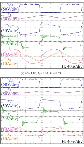
The waveforms of the proposed method are shown in Fig.
11. The magnetizing current im are derived from resonant current ir and secondary-side current. The conditions of waveforms (a) and (b) are M = 1.05, Io = 10A and M = 1.15, Io = 6A, respectively. From the drain-to-source voltage, ZVS of primary-side switches at turn-on seems to be achieved
during dead time.
The power efficiency of the DC-DC converter is shown in Fig. 12. The maximum power efficiency is 89.2%. ZVS operation has been confirmed in the range of the experimental conditions.
The temperature distribution of the prototype DC-DC converter as shown in Fig. 13, has been taken at M = 1.05 and Io = 10A. From the results, the temperature of the secondary- side is in high level, due to hard switching of the secondary- side switches. However, the power loss of the hard-switched switches in secondary-side is suppressed by using lower maximum voltage rating GaN-HEMTs of which Rds(on) is lower than that of primary-side GaN-HEMTs. Meanwhile, the primary-side temperature is relatively low because of achieving ZVS operation.
VI. CONCLUSIONS
In this paper, the principle of the proposed PWM- controlled current-mode resonant DC-DC step-down converter operated at MHz level switching frequency for high
H: 40ns/div vDS
(50V/div) vC (50V/div)
vp (50V/div)
vs (20V/div)
im (10A/div)
ir (10A/div)
(a) M= 1.05, Io = 10A, D = 0.59.
H: 40ns/div vDS
(50V/div) vC (50V/div)
vp (50V/div)
vs (20V/div)
im (10A/div)
ir (10A/div)
(b) M= 1.15, Io = 6A, D = 0.63.
Fig. 11. Experimental waveforms of resonant DC-DC converter with the proposed PWM control method.
0 2 4 6 8 10
70 80 90
Io[A]
[%]
M =1.05 M =1.15
Fig. 12. The power efficiency of resonant DC-DC converter with the proposed PWM control method.
GaN-HEMT Q1: 63C GaN-HEMT Q3: 125C Primary-side Driver : 68 C Secondary-side Driver : 95C
Diode D1: 119C Transformer Core: 41C
Secondary-side Winding : 86C Primary-side Winding : 77C
Fig. 13. The temperature distribution that temperature region is from 20C to 130C of resonant DC-DC converter with the proposed PWM control method at M= 1.05, Io = 10A, D = 0.59.