九州大学学術情報リポジトリ
Kyushu University Institutional Repository
High-Speed Optical Mode Switch Using Refractive Index Change Based on Current Injection
リアン, イマンシャ
http://hdl.handle.net/2324/1959146
出版情報:九州大学, 2018, 博士(学術), 課程博士 バージョン:
権利関係:
High-Speed Optical Mode Switch Using Refractive Index Change Based on
Current Injection
Interdisciplinary Graduate school of Engineering Science, Kyushu University
Hamamoto Laboratory August, 2018
Ryan Imansyah
© 2018
Ryan Imansyah
ALL RIGHTS RESERVED
Abstract
Conventional electrical router experiences a severe problem in power consumption especially for sustaining the future demand of data traffic.
Optical switch is attractive because it will decrease the power consumption of the router by eliminating the optical-electrical-optical (OEO) signal exchange.
One of the optical switch is based on Si-wire waveguide, known as the optical spatial switch. One of the advantage by using Si-wire waveguide is the possibility to realize revolution of on-chip communication. Moreover, silicon photonics can deliver dense footprint and also nanosecond scale reconfiguration time using electro-optic phase shifter. However, scalability for high integration of this optical switch become the main challenges to realize the optical switching. It works based on the optical input and output ports, thus, it needs the S-bend region for fiber array connection although the dimension of switching element is reduced by the latest silicon photonics technology. To overcome this issue, we proposed optical mode switch.
Optical mode switch can be realized because the optical mode that is orthogonal with each other can be mux/demux. Differently with the optical spatial switch, it only requires a single few-mode fiber (FMF) or multi-core fiber (MCF) connection in the both input and output port. Thus, the matrix size limitation issue of the high integration in the optical spatial switch can be
improved. So far, we have demonstrated the device principle by utilizing the passive device.
The electrically controlled mode switch has been demonstrated with the mode crosstalk of approximately -10 dB for 1550 nm wavelength with the injection current of 60 mA (5.7V) for the TE mode. While the mode-switching time of 2×2 silicon optical mode switch by using p-i-n trench structure was 40 ns for first order mode to fundamental mode, and a switching time of 60 ns for fundamental mode to first order mode. This switching time can be improved by optimize the p-i-n trench structure as the main part to shift the phase of the fundamental mode in one of the arms. The improvement can be done by optimize the trench dimension, increasing the dose level, and optimize the implantation energy.
Acknowledgments
First and foremost, I want to thank my supervisor Prof. Kiichi Hamamoto for the acceptance to be his student and the continuous support of my study in Kyushu University since I took my Master until I finished my Ph.D. He has taught me, both consciously and unconsciously, how the experiment of optical mode switch is done. I appreciate all his contributions of time and ideas to make my Ph.D. experience productive and stimulating. I am also thankful for his help to start the career after I finished the study in Kyushu University.
I want also to thank my co-supervisor Prof. Haisong Jiang for the guidance and help to accomplish my study in Kyushu University. With her kindness and patient, she has helped me in so many ways for my study and experiments. I am also thankful for the excellent example of multilingual person, it motivates me to be fluent in Japanese and learn other languages.
Besides my supervisor and co-supervisor, I would like to thank the rest of my thesis committee: Prof. Kiichiro Uchino and Prof. Kazutoshi Kato, for their insightful comments and encouragement, but also for the question wich incented me to widen my research from various perspective.
I also want to thank my lab rotation supervisors: Prof. Hiroshi Nakashima and Prof. Shiyoshi Yokoyama, for accepting me to be a part of their
knowledge in this field.
The members of Opto-electronic Hamamoto Laboratory have contributed immensely to my personal and professional time at Kyushu University. The group has been a source of friendships as well as good advice and collaboration. I am especially thankful for the collaboration of Optical Mode Switch group members to do the study and experiment with me : Tatsushi Tanaka, Himbele Luke, Oe Shota, and Satoshi Ogawa. I also want to thank Wenying Li and Bingzhou Hong who came in the same time to Japan with me five years ago, they helped me a lot to survive in Japan with those kanjis that I don`t know. I adore their hard work and motivation. I also want to thank Mr. Yasuhiro Hinokuma for his help to do my experiments and study.
My fellow office mates: M. Nassirudin, Ahmad Syahrin, and Mahmoud Nasef.
I very much appreciated their kindness, helped, and support during my study, and also their patient towards my noisy and messy table. Other present laboratory members that I have had the pleasure to work with or alongside of are grad students Yu Han and Zanhui Chen; master students Tomotaka Mori, Kantaro Fujimoto, Ryota Kuwahata, and Shingo Murakami; undergraduate students Keisuke Iwasaki and Tomoya Zennoji. I also want to thank the past laboratory member Yutaka Chaen, Hirohito Hokazono, and Kazuhiro Tanabe for their help during my first year in Japan, not to mention their help towards my experiments and study.
For the study in Kyushu University I would like to thank the Green Asia (GA) program, the GA professors: Mr. Andrew Spring, Mr. Keisuke Yamamoto,
Mr. Hiroshi Furuno, and Ms. Naoko Mae, for their guidance during my journey in GA program. Not forget the GA staffs: Ms. Yuko Hayashi, Ms. Yoshiko Kano, Ms. Yu Kazekita, Ms. Ishibashi, Ms. Shiragaki, Ms. Inoue, and Mr. Makino, for their help towards my completion in every activity for GA program. Especially Ms. Yuko Hayashi that helped me a lot to survive in Japan including preparing the things for getting a job, improving my Japanese skill, and her suggestion in a hard time.
My time at Kyushu University was made enjoyable in large part due to the many friends and groups inside and outside Kyushu University that became a part of my Life. I am grateful for time spent with them, Su Liwen, my twin sister different parents. Alisa Banaron, we just known each other less than 3 years yet feels like already a decade. The GA students in the same batch: Zayda Faizah Zahara, Azizah Intan, Sendy Dwiki, and Pennapa Tungjirattitikan, it’s such a journey to complete the study with you. The fellow Indonesian students: Dalton, Ayu, Halim, Adit, Etika, Aam, and Aji, for the kindness that made Japan feels like home. The Thai students that I always had the lunch together: Kurrapha, Iize, and Phum, for the talks and laughs during lunch. My friends other friends that I met in Japan: Riya, Farina, Hong, David, John, Radit, Hiroko, and Howard. Thank you for your support and the time that we spent and making my life more colorful. Not to forget as well my grateful to all my best friends in Indonesia: Melissa, Ardhini, Chairul, Nalendra, Diatri, Andika, and Via.
Lastly, I would like to thank my family for all their love and
encouragement. For my parents who raised me with a love, always praying for me, and supported me in all my pursuits. For my sister and her husband who always taking care my parents while I was not presence at home during my study. My nephew and niece who gave me a reason to work hard and do my best. The Yusuf family and Dirmansyah family who always supporting me and praying for me. Thank you.
Ryan Imansyah Kyushu University August 2018
Table of contents
Abstract iii
Acknowledgments v
Chapter 1 Introduction 1
1.1 Background: Challenges of the present data center networking
2 1.1.1 High power consumption 2
1.1.2 Limited scalability 3
1.1.3 Space management 4
1.1.4 High Latency 4
1.2 Proposed solution: optical mode switch for faster switch and scalable
architecture
5
1.2.1 Ultra high capacity 5
1.2.2 Low power consumption 5
1.2.3 Small footprint 6
1.3 Optical mode switch: state of the art 9
1.4 Thesis construction 11
1.5 References 12
Chapter 2 Two Modes Optical Mode Switch Design 19 2.1 Mode division multiplexing 19
2.2 Device configuration 20
2.2.1 Mode combiner 20
2.2.2 Trench p-i-n structure 27
2.3 Preliminary mode switch using different arm’s length structure
31
2.4 Conclusions 33
2.5 References 34
Chapter 3 Mode Evaluation Method 36
3.1 2×2 MMI mode filter 39
3.2 1×3 MMI mode filter 41
3.3 Results and discussion 43
3.4 Conclusions 48
3.5 References 49
Chapter 4 Mode-Switching Time of 2×2 Optical Mode Switch
51 4.1 P-I-N trench fabrication process 51 4.2 Ion implantation distribution 54
4.3 Atoms diffusion in Si 57
4.4 Results and discussion 61
4.5 Conclusions 76
4.6 References 76
Chapter 5 Conclusion and Outlook 78
5.1 Conclusion 78
5.2 Outlook 80
List of symbol 81
List of abbreviation 84
Chapter 1 Introduction
The rise of cloud computing and other web applications induces data storage to be centralized in data centers. This idea of using data centers to form a seamless infrastructure capable of running applications and storing data remotely will make the Internet Protocol (IP) traffic to grow exponential pace continuously. It is following the proliferation of smart mobile devices and driven by increasing demands for multimedia, video-on-demand, and other data services [1,2]. It makes Data Center (DC) networks are suffering from the growing demands, various applications and virtualization trends [3-5].
This condition has created the communication traffic to/from data center getting higher, the demand of interconnection network in data centers increased, and also more powerful large-scale of data centers is needed. It is expected that the projected future interconnection network traffic cannot be sustained without consuming the excessive amount of power. Thus, the data center need to be improved in order to support the very large scales of internet traffic while also keep the footprint and lower the power consumption. To overcome these problems due to the hardware limitations of electrical DCs, optical switching has been investigated in several projects to realize the all-optical networks [6-8].
The objective of this thesis is to develop the all-optical network system
keeping the low scale and higher energy efficiency. Following the ongoing research of data center network design, we aim to use the mode division multiplexing (MDM) for the scalability and energy efficiency improvement.
1.1 Background: Challenges of the present data center networking
The recent DCs are organized in a multi-tier topology where the electronic switches are used for the interconnection between groups of servers and top-of-rack (ToR). However, there is a limitation of I/O bandwidth due to the use of a ball grid array (BGA) in the hardware package [9].
Moreover, by using the conventional electronic switches, optical-to-electrical and electrical-to-optical (OEO) converter is needed, which leads to high power consumption, limited scalability, and also high latency.
1.1.1 high power consumption
The excessive amount of power consumption is one of the most challenging to maintain the demand of future internet traffic. The estimation from a green peace report said that the global demand for electricity from data centers will be triple from 330 billion kWh in 2007 to more than 1000 billion kWh in 2020 [10]. Fig 1 shows the breakdown of energy consumption by different components of a data center [11].
It shows that server and storage and also network hardware spend 26%
and 10% of the total power, respectively. The network seems only spent 36% of the total power, however, the electronic and switch in the
conventional data center taking part for the consumption from the cooling system. A single switch in higher data center network tiers can consume more than ten kilowatts if cooling system also being considered [12].
Fig. 1. A breakdown of energy consumption by different components of a data center [11]. Most of the cooling is needed for the electronic and switch
part of the data center.
1.1.2 Limited scalability
According to Cisco, the annual global data center will reach 20.6 Zettabytes (ZB) or 1.7 ZB per month by the end of 2021, up from 6.8 ZB per year or 568 exabytes (EB) per month in 2016 [13]. However, the architecture based on Ethernet links and switches has a limited capacity to manage this traffic flowing within data centers. The data center network also will be hard pressed by the technology trends and seems
50%
26%
10%
11% 3%
Cooling Server and storage Network hardware Power conversion Lighting
that the Moores’s law seems to be applicable to increase the performance for the near future [14].
1.1.3 Space management
In order to follow the demand of future internet traffic, nonblocking data center connectivity is needed. It would require a massive amount of Ethernet cables when the data center should accommodate millions of server cores [14]. It will lead to severe implementation, management, and maintenance problems.
1.1.4 High latency
The conventional routers yield a relatively high and variable latency or delay, thus, it is not capable of supporting many multimedia applications. Which means they are also incapable to operate at the gigabit speeds. Meanwhile, the oversubscription ratio is increased rapidly. Oversubscription is defined as the ratio of the worst-case achievable aggregate bandwidth among the end hosts to the total bisection bandwidth of a particular communication topology [15]. For examples, servers are able to communicate within the rack at the full rate of their interfaces [14]. Uplink from ToRs are typically 5:1 to 20:1 oversubscription, or 2 to 8 Gbps uplink for 40 servers [16]. Paths through the highest layer of the tree may even be 240:1 oversubscribed [16, 17].
1.2 Proposed solution: optical mode switch for faster switch and scalable architecture
To overcome these problems due to the hardware limitations of electrical DCs, optical switching has been investigated in several projects to realize the all-optical networks [6-8]. The purpose is to overcome the power issue and electrical-to-optical (OEO) signal exchanges problem in the conventional router, OEO switching process has a low latency of ns order switching [18]. There are three major properties of optical transmission technology: ultra-high capacity, low power consumption, and small footprint.
1.2.1 Ultra high capacity
One of the problems in optical signal processing is the capacity of single-mode fiber that almost reaches the physical limit of 100 Tb/s.
There are several digital signals processing (DSP) method that can accommodate the explosive growth of data communication traffic.
These methods are Time Division Multiplexing (TDM), Spatial Division Multiplexing (SDM), Wavelength Division Multiplexing (WDM) and Mode Division Multiplexing (MDM). These techniques can be realized by using the multi-core fibers (MCF) and multi-mode fibers (MMFs) as a form of multi-input multi-output (MIMO) transmission [19-21].
1.2.2 Low power consumption
Low power consumption is one of the major characteristics of optical links and switches [22-24]. Optical switching technology has a
consumes power independent of the bandwidth of the signal it switches [14]. As the result, power per unit bandwidth in optical switches could be lower than the electronic switches.
1.2.3 Small footprint
A fiber optic has only a diameter of 125 µm, however, it has a significant capacity to provide. Optical switching components could be built very compact through photonic integration [14]. However, minimize the cable installation in the data center architecture is needed in order to make the installation, management, and maintenance more efficient.
In the conventional SDM, optical transmission is currently utilized in data centers only for some point-to-point links on multimode fibers. To extend the capacity a new installation of fiber is needed, however, there are not so many rooms left for it. As already mentioned in 1.2.1, There are several DSP methods that can accommodate the explosive growth of data communication traffic. These methods are attractive because it can be realized by using the MCF and MMFs as a form of MIMO transmission [19-21].
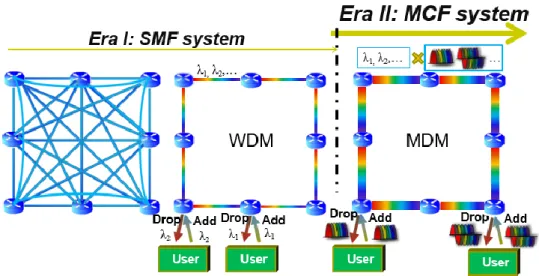
For example, WDM with ring topology is attractive because it doesn’t need to be connected with each other while still accommodate a massive data communication traffic. However, to keep increasing the capacity, the MDM combine with WDM has been studied. In here to treat the modes, optical mode switches and add/drop multiplexer are needed. Figure 2 shows the
evolution of router connection architecture. While the add/drop multiplexer is shown in fig. 3.
Fig. 2. The evolution of router connection architecture. The combination of MDM and WDM will increase the capacity of communication traffic.
Fig. 3. Add/drop multiplexer in optical mode switch architecture. Add drop is needed to connect each user with the main line of ring topology.
The focus in this research is to design a data center network for the next generation of optical switching by using the MDM with a ring topology.
However, there are so many steps to be done to realize this system. In the beginning, the study of optical mode switch is discussed in this thesis.
There are several types of optical switch, optomechanical switches [25], micro-electro-mechanical systems (MEMS) switches [26, 27], electro-optic switches [28], thermo-optic switches [29], liquid-crystal switches [30], bubble switches [31], semiconductor optical amplifier switches [32], and fiber bragg grating based switches [33,34]. The application is different from each other, depends on the needs for a telecommunication system. From all the types of optical switch, waveguide-based optical space switch is more attractive because it can utilize refractive index change that may result in high-speed operation of ns order switching. It is believed that by using the optical switch, can save up to 92 percent space and 96 percent power [35].
However, the switch matrix size issue occurs on waveguide type optical space switch due to the bending waveguide region to open up toward array fiber. This problem occurs because normally it has an adjacent spacing of 125 µm, even if the size of switching elements is reduced by the latest advanced waveguide technologies including wire waveguide, silicon photonics, and photonic crystal. The other problem is the fiber nesting that is occurred because we need a lot of input port and the output port. In order to overcome the fiber nesting and the switch matrix problems in optical switching, we proposed the optical mode switch.
1.3 Optical mode switch: state of the art
Compared to a conventional optical spatial switch, the optical mode switch only needs one input and output port by employing a few-mode fiber (FMF) or a multicore fiber (MCF). A number of optical modes switches have been reported, such as the one driven by electromagnetic field [36], thermos- optically tuning waveguide with Mach-Zehnder Interferometer (MZI) structure [37], electro-optic grating Lithium Niobate (LN) waveguide [38] and an MZI structure with a phase shifter [39]. The summary of optical mode switch technology is shown in Tab. 1. However, these mode switches suffer from low switching speed, high driving voltage, and large size. On the other hand, Si-wire based optical spatial switch is attractive because of the potential for high-speed operation and low power consumption [40, 41]. Moreover, silicon photonics offers merits of dense footprint and nanosecond reconfiguration time using an electro-optic phase shifter [42, 43]. The Y- junction and multimode interference based on SOI that was done by McGill University group have a high-speed result of the two-mode switch, however, the device is integrated with the 2×2 MMI structure [44]. It makes the output of the device is fundamental modes but in the different output ports. Among these optical mode switches, we fabricated the device that has only one input port and one output port that will simplify the installation method.
Table. 1: Summary of Optical Mode Switch Year Total
modes
Structure Length
Dimension
Voltage And λ
Switching time
Ref
2013 2 Symmetric Y-
junction waveguides
- - - [45]
2014 2 Two mode fibers inside magnetic coil
100 mm 50 V for 1550 nm
- [36]
2014 2 Mach-Zehnder Interferometer waveguide by using Dow Chemical benzocyclobutene
3.5 mm - - [37]
2015 2 Long-period
waveguide grating in lithium-niobate
8 mm 35 V for 1544 nm
- [38]
2016 2 Mach-Zehnder Interferometer waveguide with one input port and output port.
1.5 mm 5.6 V 40 ns – 60 ns
[46]
2016 2 Lithium-niobate Mach-Zehnder interferometer
24 mm 3 V for 1550 nm
- [40]
2017 2 Y-junction and
multimode
interference based on SOI.
0.6 mm 1.22 V for 1550 nm
2.5 ns [44]
1.4 Thesis construction
This section provides the overview of the later chapters of this thesis.
We begin with the study of the available technologies from the research community aiming at resolving the challenges in data center networks. Our technical contribution is followed in three chapters and finally concludes the thesis.
In chapter 2, to realize the optical mode switch, 2 modes optical mode switch is proposed as the preliminary design of the optical mode switch. In this work, the theory of how to realize the optical mode switch will be discussed.
In chapter 3, in this chapter, the mode evaluation theory will be discussed. MMI mode filter was used experimentally. The mode-switching with an injection current of 60 mA (5.7 V) was successfully evaluated with mode-crosstalk of 10 dB at λ=1550 nm for the TE mode.
In chapter 4, the mode switching speed will be discussed. A minimum of less than 60 ns and 40 ns mode switching time for the fundamental mode to first order mode and vice versa, was achieved respectively.
In Chapter 5, the above results have been summarized and clarified about the future view of the proposed waveguide structure.
1.5 References
[1] K. I. Sato and H. Hasegawa, “Optical networking technologies that will create future bandwidthabundant networks," IEEE/OSA Journal of Optical Communications and Networking, vol. 1, no. 2, pp. A81.A93, Jul. 2009.
[2] M. Jinno, H. Takara, B. Kozicki, Y. Tsukishima, Y. Sone, and S. Matsuoka,
“Spectrum-e_cient and scalable elastic optical path network: architecture, benets, and enabling technologies," IEEE Communications Magazine, vol. 47, no. 11, pp. 66..73, Nov. 2009.
[3] M. Meeker and L.Wu, “2013 internet trends,” Kleiner Perkins Caufield &
Byers, Technical Report (2013).
[4] S. Sakr, A. Liu, D.M. Batista, and M. Alomari, “A survey on large scale data management approaches in cloud environments,” IEEE Com. Sur. & Tut., vol.
3, no. 13, p. 311-336, Sept. 2011.
[5] Cisco Systems Inc., “Cisco global cloud index: Forecast and methodology 2013–2018 white paper,” 2014.
[6] C. Kachris and I. Tomkos, “A Survey on Optical Interconnects for Data Centers,” IEEE Communications Surveys & Tutorials, vol.14, no.4, pp.1021- 1036, 2012.
[7] N. Farrington, G. Porter, S. Radhakrishnan, H. H. Bazzaz, V. Subramanya, Y.
Fainman, G. Papen, and A. Vahdat, “Helios: a hybrid electrical/ optical switch architecture for modular data centers,” in Proceedings of the ACM SIGCOMM 2010, pp. 339–350, 2010.
[8] X. Ye, Y. Yin, S. J. B. Yoo, P. Mejia, R. Proietti, and V. Akella, “DOS: A scalable optical switch for datacenters,” in Proceedings of the 6th ACM/IEEE Symposium on Architectures for Networking and Communications Systems, ser. ANCS ’10, pp. 24:1–24:12, 2010.
[9] A. Ghiasi, “Is there a need for on-chip photonic integration for large data warehouse switches,” Proc. 9th IEEE Int. Conf. Group IV Photon., San Diego, CA, pp. 27-29, Aug. 2012.
[10] Greenpeace International, “Make IT green: cloud computing and its contribution to climate change." [Online]. Available:
http://www.greenpeace.org/, Mar. 2010.
[11] Info-Tech, “Top 10 energy-saving tips for a greener data center,” Info- Tech Research Group, London, ON, Canada, Apr. 2010. [Online]. Available:
http://static.infotech.com/downloads/samples/070411_premium_oo_green dc_top_10.pdf
[12] W. Zhang, H. Wang, and K. Bergman, “Next-generation optically- interconnected highperformance data centers," IEEE/OSA Journal of Lightwave Technology, vol. 30, no. 24, pp. 3836-3844, Dec. 2012.
[13] Cisco global cloud index: “forecast and methodology, 2016-2021."
[Online]. Available: http://www.cisco.com/, Apr. 2017.
[14] H. Rastegarfar, “Optical Switching in Next-Generation Data Centers,”
Thesis paper, University of Toronto, 2014.
[15] M. Al-Fares, A. Loukissas, and A. Vahdat, “A scalable, commodity data center network architecture," in ACM SIGCOMM'08, pp. 63.74, Aug. 2008.
[16] A. Greenberg, J. R. Hamilton, N. Jain, S. Kandula, C. Kim, P. Lahiri, D. A.
Maltz, P. Patel, and S. Sengupta, “VL2: a scalable and exible data center network," in ACM SIGCOMM'09, vol. 39, pp. 51{62, Aug. 2009.
[17] K. Nagaraj, H. Khandelwal, C. Killian, and R. R. Kompella, “Hierarchy- aware distributed overlays in data centers using DC2," in Fourth International Conference on Communication Systems and Networks (COMSNETS), pp. 1.10, Jan. 2012.
[18] J. V. Campenhout, William M. J. Green, S. Assefa and Y. A. Vlasov, “Low- power, 2x2 silicon electro-optic switch with 110-nm bandwidth for broadband reconfigurable optical networks,” Opt. Express, vol. 17, No. 26, pp. 24020- 24029, 2009.
[19] T. Morioka, Y. Awaji, R. Ryf, P. J. Winzer, D. Richardson, and F. Poletti,
"Enhancing optical communications with brand new fibers," IEEE Commun.
Magazine, vol.50, no.2, pp. s31-s42, Feb. 2012.
[20] P. J. Winzer and G. J. Foschini, “MIMO capacities and outage probabilities in spatially multiplexed optical transport systems,” Opt. Express., vol. 19, no.
17, pp. 16680–16696, Aug. 2011.
[21] R. Essiambre and R. W. Tkach, "Capacity Trends and Limits of Optical Communication Networks," Proc. of the IEEE , vol.100, no.5, pp.1035-1055, May 2012.
[22] D. A. B. Miller, “Device requirements for optical interconnects to silicon chips," Proceedings of the IEEE , vol. 97, no. 7, pp. 1166.1185, Jul. 2009.
[23] A. Shacham, K. Bergman, and L. P. Carloni, “Photonic networks-on-chip for future generations of chip multiprocessors," IEEE Transactions on Computers , vol. 57, no. 9, pp. 1246.1260, Sep. 2008.
[24] S. J. B. Yoo, “Optical packet and burst switching technologies for the future photonic Internet,"IEEE/OSA Journal of Lightwave Technology , vol. 24, no. 12, pp. 4468.4492, Dec. 2006.
[25] S. Nagaoka and Y. Suzuki, “Compact optomechanical switches and their applications in optical communication and testing systems,” in Proceedings of MEMS 1997, IEEE, pp. 366-371.
[26] D. J. Bishop, C. R. Giles, and S. R. Das, “The rise of optical switching,” Sci.
Amer., vol. 284, no. 1, pp. 88–94, Jan. 2001.
[27] J. E. Ford, “Optical MEMS: Legacy of the telecom boom,” in Proc. Solid State Sensor, Actuator and Microsyst. Workshop, Hilton Head, SC, Jun. 6–10, pp. 1–3, 2004.
[28] Z. L. Samson, K. F. MacDonald, F. De Angelis, B. Gholipour, K. Knight, C. C.
Huang, E. Di Fabrizio, D. W. Hewak, and N. I. Zheludev, “Metamaterial electro- optic switch of nanoscale thickness,” Applied Physics Letters 96, 2010.
[29] E. A. Camargo, H. M. H. Chong, and R. M. De La Rue, “2D photonic crystal thermo-optic switch based on AlGaAs/GaAs epitaxial structure,” Optic Express 12, 4, pp. 588-592. 2004.
[30] Riza, N.A. and S.F. Yuan, “Reconfigurable wavelength add-drop filtering based on a Banyan network topology and ferroelectric liquid crystal fiber- optic switches.” IEEE Journal of Lightwave Technology, 17(9): p. 1575-1584, 1999.
[31] Jackel, J.L., J.J. Johnson, and W.J. Tomlinson, “Bistable Optical Switching Using Electrochemically Generated Bubbles,” Optics Letters, 15(24): p. 1470- 1472, 1990.
[32] Renaud, M., M. Bachmann, and M. Erman, “Semiconductor optical space switches,” IEEE Journal of Selected Topics in Quantum Electronics, 2(2): p.
277-288, 1996.
[33] Ball, G.A. and W.W. Morey, “Tunable Bragg grating fiber filters and their applications,” in Conference on Lasers and Electro-Optics (CLEO). 1997.
[34] Melloni, A., M. Chinello, and M. Martinelli, “All-optical switching in phase- shifted fiber Bragg grating,” IEEE Photonics Technology Letters, 12(1): p. 42- 44, 2000.
[35] Laura, “ABCs of optical switch,” Fiber optic equipment solutions, FS.com, May 27, 2016. [online]. Available : http://www.fiber-optic- equipment.com/abcs-of-optical-switch.html
[36] H. Sakata, H. Sano, and T. Harada, “Tunable mode converter using electromagnet-induced long period grating in two-mode fiber,” Opt. Fiber Technol., vol.20, no.3, pp.224–227, 2014.
[37] W.Y. Chan and H.P. Chan, “Reconfigurable two-mode mux/demux device,” Opt. Express, vol.22, no.8, pp.9282–9290, 2014.
[38] W. Jin and K.S. Chiang, “Mode switch based on electro-optic long-period waveguide grating in lithium niobate,” Opt. Lett., vol.40, no.2, pp.237–240, 2015.
[39] M. Zhang, K. Chen, W. Jin, and K.S. Chiang, “Electro-optic mode switch based on lithium-niobate Mach-Zehnder interferometer,” Appl. Opt., vol.55, no.16, pp.4418–4422, 2016.
[40] T. Barwicz, H. Byun, F. Gan, C.W. Holzwarth, M.A. Popovic, P.T.
Rakich,M.R.Watts, E.P. Ippen, F.X. K¨artner, H.I. Smith, J.S. Orcutt, R.J. Ram, V.
Stojanovic, O.O. Olubuyide, J.L. Hoyt, S. Spector, M. Geis, M. Grein, T.
Lyszczarz, and J.U. Yoon, “Silicon photonics for compact, energy-efficient interconnects [invited],” J. Opt. Netw., vol.6, no.1, pp.63–73, 2007.
[41] H. Yamada, T. Chu, M. Tojo, S. Nakamura, M. Tokushima, Y. Urino, S.
Ishida, and Y. Arakawa, “A compact optical switch module with Si-wire waveguides,” 4th IEEE International Conference on Group IV Photonics 2007 (GFPIV2007), pp.119–121, 2007.
[42] J. Xing, Z. Li, P. Zhou, X. Xiao, J. Yu, and Y. Yu, “Nonblocking 4 × 4 silicon electro-optic switch matrix with push-pull drive,” Opt. Lett., vol.38, no.19, pp.3926–3929, 2013.
[43] B.G. Lee, A.V. Rylyakov, W.M.J. Green, S. Assefa, C.W. Baks, R. Rimolo- Donadio, D.M. Kuchta, M.H. Khater, T. Barwicz, C. Reinholm, E. Kiewra, S.M.
Shank, C.L. Schow, and Y.A. Vlasov, “Monolithic silicon integration of scaled photonic switch fabrics, CMOS logic, and device driver circuits,” IEEE J.
Lightwave Technol., vol.32, no.4, pp.743–751, 2014.
[44] Y. Xiong, R. B. Priti, and O. L-Ladouceur, “High-speed two-mode switch for mode-division multiplexing optical networks,” Optica., vol.9, no.9, pp.1098-1102,2017.
[45] M. Jizodo, A. Fujino, and K. Hamamoto, “Proposal of Optical Mode Switch Using Symmetric Y-junction Waveguides,” Tech. Dig. IEEE 18th OptoElectronics and Communications Conference held jointly with 2013 International Conference on Photonics in Switching (OECC/PS), pp. 1-2, Kyoto, 2013,.
[46] H. Jiang, R. Imansyah, L. Himbele, S. Oe, and K. Hamamoto, “Fast Mode- Switching (60 ns) by Using a 2×2 Silicon Optical Mode Switch,” IEICE Trans.
Electron., vol.E100-C, no.10, pp.782–788, 2017.
Chapter 2
Two Modes Optical Mode Switch Design
2.1 Mode division multiplexing
Mode Division Multiplexing (MDM) is employing the advantage of multi-mode fiber to transmit a different kind of optical modes. The idea is almost the same as Wavelength Division Multiplexing (WDM), however, the source is varied by optical modes. Optical modes can be easily multiplex and demultiplex by using the directional coupler on the silicon-on-insulator platform [1]. However, to optimize the performance of MDM, group delay spread and mode-dependent loss and gain should be considered.
Figure 1. Schematic of MDM with three different modes. It’s only need at least one multi-mode fiber in MDM configuration. The modes can be
switched by using optical mode switch.
Figure 1 shows the schematic of MDM with three different modes. The signals from multiple senders are transmitted as fundamental mode, however, the signals then propagate as different modes after the multiplexer.
Then, the signals are sent to each destination as a fundamental mode with the help of demultiplexer. Thus, by implementing this schematic of MDM, optical mode switch can accommodate both high switching speed and also high capacity of data traffic.
2.2 Device configuration
In order to realize the optical mode switch, high switching speed is not only the important characteristic that needs to be achieved. The high output power is also beneficial in order to get a clear signal transmission. Thus, the device configuration is also needed to be optimize. There are two important parameters for the structure, mode combiner and p-i-n trench structure, in order to optimize the output power of the signals.
2.2.1 Mode combiner
Figure 2 shows a schematic of the optical mode switch for the fundamental-mode and the first-order mode. As shown, the configuration is similar to that of a Mach-Zehnder interferometer, however, there is a difference in the waveguide width of the Y-junction connected to the two single-mode waveguides [2]. Here, we use the symmetric Y-junction that is suitable for equal power splitting [3-6]. The width of the waveguide at the Y-
junction is designed to be twice of the arm’s width to realize mode combining for the fundamental mode as well as the first-order mode. On the other hand, to realize mode switching, we designed the symmetrical arms with a refractive index change region in one of the arms. We injected electrical current to this region to generate a π-phase difference between arms.
Fig.2. Optical-mode switch configuration. Input and output signals are in the form of fundamental mode and first-order mode with the same
input and output port.
When the fundamental mode is injected in the input port, it is going to split into two fundamental modes with the same phase at the 3 dB splitter.
While when the first-order mode is injected, it is split into two fundamental modes with phase π difference each other. Figure 2 shows the beam propagation method (BPM) simulation results of the optical mode switch between fundamental mode and first-order mode. When the phase shifter is the bar-state Fig. 3.a, the modes propagate and then couple at the mode coupler into the same modes as the injected modes. When a certain current is injected into the phase shift region and the phase shifter is cross-state Fig.
3.b, the phase of the one split fundamental mode is shifted with π. Thus, these are coupled as the first-order mode at the end. Meanwhile, the injected first-
order mode is converted into the two fundamental modes in the same phase, and then couple as the fundamental mode. Thus, this structure realizes the switching between the fundamental mode and the first-order mode. In such a way, both modes are switched each other simultaneously.
Fig. 3. Simulation results for the (a) bar state and (b) cross state. Bar state shows the condition when there is no π phase shift in one of the arms, while
cross state shows the condition when there is a π phase shift in one of the arms.
By injecting the electrical current, the concentration of free charges in silicon changes the refractive index of the material, thus, the phase of the light can be shifted. The relationship between refractive index changes in silicon and the injection of carriers in silicon at 1.55 µm wavelength is expressed by Soref and Bennet using experimental data [7]. This equation is almost universally used for the evaluation of optical modulation in silicon:
∆𝑛 = ∆𝑛𝑒 + ∆𝑛ℎ = −8.8 × 10⁻²²∆𝑁𝑒 − 8.5 × 10⁻¹⁸(∆𝑁ℎ)0.8, (1)
where Δne and Δnh are the changes in the refractive index resulting from the change in free electron carrier concentration (ΔNe) and free hole carrier concentration (ΔNh), respectively.
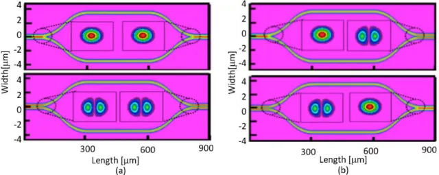
Fig.4. Schematic of the mode combiner and its propagation field for the same phase between arms. (a) Propagation of light from left arm and (b) right arm, and (c) how the lights combine into the fundamental mode after
the Y-junction.
Figures 4(a) and 4(b) show the propagation of light in a multimode waveguide after the Y-junction from each arm in the case of the phase of the light at each arm is the same. As shown in the figure, light from one arm propagates in a zig-zag manner [8]. This phenomenon is considered as follows (similar to mode-coupled theory): i) light from one arm is considered as a combination of even and odd modes at the starting point of the multimode waveguide; ii) owing to the propagation constant difference between even and odd-modes, the peak of the combination moves left and right along the direction of propagation; iii) as a result, the light propagates in a zig-zag manner, as shown in Figs. 4(a) and 4(b). This zig-zag propagation occurs for both cases of Fig. 4(a) and 4(b), however, there is the difference between odd
(a) (b) (c)
different by π [rad], while they are the same for even modes. Hence, the resulting optical field goes into the regular single mode, as shown in Fig. 4(c).
Fig.5. Schematic of the mode combiner and its propagation field for π phase difference between arms. (a) Propagation of the light from left arm and (b) right arm, and (c) how the lights combine into the first-order mode after the
Y-junction.
Now, let us consider the case of π phase shift in one arm (Fig. 5). The phenomena that occur at the same Y-junction is considered as follows: i) light from one arm is considered to be a combination of even and odd modes at the starting point of the multimode waveguide; ii) because of the propagation constant difference between even and odd modes, the peak of the combination moves left and right along the direction of propagation; iii) as a result, the light propagates in a zig-zag manner, as shown in Figs. 5(a) and 5(b).
This zig-zag propagation occurs in both cases of Figs. 5(a) and 5(b), however, in this case, the phases of “even” modes in each arm are different by π [rad]
while the phases are the same for “odd” modes. So, the resulting optical field becomes the first-order mode, as shown in Fig. 5(c).
(b) (c)
(a)
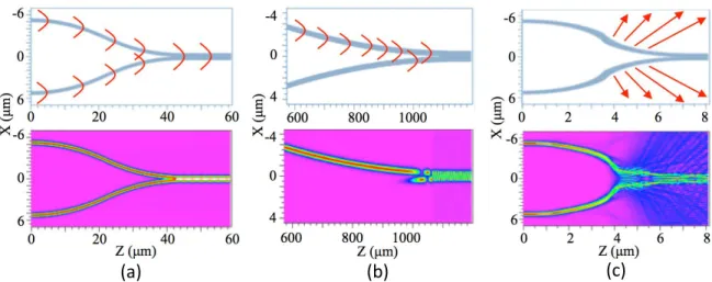
Fig. 6. Schematic and propagation field in mode combiner with the distance between arms of 10 µm: (a) 8 µm < r < 16000 µm, (b) r ≥ 16000
µm, and (c) r ≤ 8 µm. These pictures shows that the undesired coupling when the r is too large and a high loss when it is too small.
To realize a proper mode-combiner based on the Y-junction with two S- bend waveguides as shown in Fig. 6 (a), there may be two critical issues that must be overcome: 1) one is undesired coupling between adjacent waveguides before light propagates into the multimode waveguide, and 2) the other is radiation loss, as explained below.
i. Undesired coupling occurs when bending radius R is too long, as shown in Fig. 6(b). This may degrade the mode. However, the significant undesired coupling is avoided easily when r satisfies r < 16000 µm.
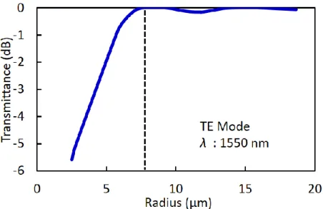
ii. Radiation loss may occur when r is too short [see Fig. 6(c)]. Figure 7 shows the radiation loss as a function of r estimated by the finite domain time difference method (FDTD). Significant radiation is generated when r ≤ 8 µm, as shown in the figure.
(a) (b) (c)
Fig. 7. Output power for short bending radius (r≤ 8 µm) estimated by FDTD method. It shows that above 8 µm, the bending loss is almost zero.
Fig. 8. Opening space of 70 µm for silicon doping between arms of an actual device. This opening space is necessary in order to make the
doped region for the phase shifter.
According to these results, the bending radius of 8 µm < r < 16,000 µm is the design criteria for the mode combiner. For the actual device, we designed r to be 610 µm to make a distance of 70 µm between arms for the opening space of ion implantation, as shown in Fig. 8. This distance is used to ensure sufficient space for wire bonding on top of the electrodes.
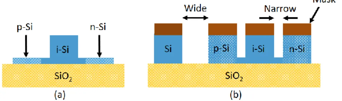
2.2.2 Trench p-i-n structure
In order to realize the optical mode switch, we fabricated a p-i-n structure in the phase shifter region. In here intrinsic silicon (i-Si) is the waveguide part, thus it is essential to keep the propagation loss low. Thus, p- type and n-type regions must be connected to the waveguide in a lateral direction, as shown in Fig. 9(a), while the other region is fully etched. Thus, at least, a two-step dry etching process is needed. To simplify the fabrication into a one-step etching process, we fabricated a p-i-n trench structure by utilizing the aspect-ratio-dependent etching (ARDE) phenomenon [9, 10]. The silicon etches rate decreases as the open space size decreases. The illustration of wide and narrow open spaces when making a trench structure is shown in Fig.
9(b). A slight amount of the remaining Si layer bridges the p-doped region and the waveguide, as well as the n-doped region and the waveguide, for narrow open spaces. Thus, the p-i-n structure is realized by this technique.
Fig. 9. Cross-section of p-i-n structure. (a) Conventional p-i-n structure and (b) p-i-n trench structure. The narrow opening space has lower etching
rate than the wide opening space, thus, two different depths can be made.
Fig. 10. Propagation field profiles at the trench region. (a) Non-leaky condition and (b) leaky condition. It shows that too shallow trench will
increase the propagation loss of the device.
However, one critical issue of the trench structure is its radiation loss toward the trench direction due to the relatively low refractive index contrast in the lateral direction that may cause leaky-mode propagation. Figure 10 shows example propagation field profiles of (a) non-leaky condition and (b) leaky condition at the trench region. As shown in the figure, if the trench region is designed as a leaky condition with a shallow trench, significant radiation happens that causes huge loss while deep trench prevents this radiation as shown in Fig. 10 (b). To side-step this radiation issue at the trench, we verified the design criteria of this region.
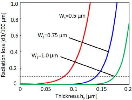
Fig. 11. The radiation loss as a function of thickness of remaining silicon layer. It shows that the narrower of the trench width Wt, the lower
fabrication tolerance for the remaining thickness of hs.
Figure 11 shows the radiation loss as a function of the thickness of the remaining silicon layer hs. Wt is the trench width and hs is the thickness of the remaining silicon layer. As can be seen in Fig. 11, the radiation loss is reduced as the trench width Wt increased. When Wt is 0.50 μm and hs is less than 0.08μm, the radiation loss is suppressed below 0.1 dB/100 μm. The upper limit of hs increases as Wt increases, thus, manufacturing tolerance is also significantly improved. Based on these design criteria with sufficient fabrication tolerance, we decided to fabricate hs of 30 nm to suppress the radiation loss with setting Wt to be 0.8µm in this work.
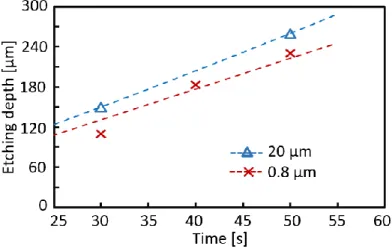
Before we fabricated the p-i-n trench structure, we investigated the etching rate as a function of open space size. We designed two sizes of open
spaces; 0.8 µm and 20 µm, on the basis of silicon-on-insulator (SOI) rib waveguides. The structure was etched using inductively coupled plasma (ICP).
Fig. 12. The etching rate as a function of the opening space size. It shows that the narrow opening space (0.8 µm) has lower etching rate.
Fig. 13. Trench for p-i-n structure. Cross sections of (a) narrow opening (0.8 μm) and (b) wide opening (20 μm). It shows that a different of 30
nm between narrow opening space and wide opening space can be made in the same etching process.
Figure 12 shows the etching rate as a function of open space size. As can be seen in the figure, the etching rate decreases as the open space size decrease. As shown in Fig. 13(a), 30 nm of Si layer remained as the connector of the waveguide to both the p-doped and n-doped regions after single-step
2.3 Preliminary mode switch using different arm’s length structure
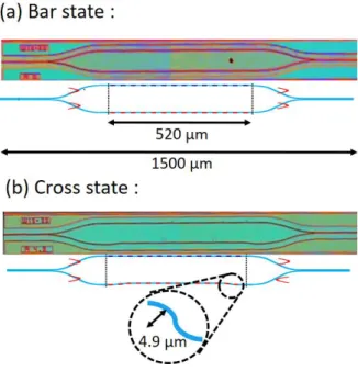
In order to verify the basic operation principle of the optical mode switch, cross state device with a different arm’s length corresponding to the refractive index conversion region was fabricated on the same substrate. The bar state device with symmetrical arm’s length, was also fabricated. These devices were confirmed to be able to inter-mode switching.
To evaluate the mode crosstalk, instead of realizing the phase-shift region based on current injection, we fabricated physical length different devices in the arms [2]. Figure 14 shows the top view of the implemented devices. As can be seen in Fig. 14(a), the device has the same arm length to confirm bar-state. Meanwhile, the device has bending regions in one arm to have a π phase shift between two arms to confirm cross-state. The devices were fabricated using silicon-on-insulator (SOI) wafers with 2 µm thick buried oxide layer (lower cladding layer) and 300 nm top Si layer (core layer).
Fig. 14. Top view of (a) symetrical arm and (b) the length different arms device. These device is needed as the preliminary experiment of optical
mode switch.
The device was implemented by using inductively coupled plasma (ICP) dry etching technique. At the final process, the surface of the device was covered with SiO2 using plasma chemical vapor deposition method. The implemented device geometries are summarized in Tab. 1.
Tab. 1 Device geometries Dimension
Length 1500 µm
Input output
width 3 µm
Arm Width 1.5 µm Arm Length 520 µm
Radius 4.9 µm
Length different 0.26 µm
Fig. 15. Waveguide (a) without optical path difference and (b) with optical path difference. It shows the NFP from the bar state and cross state of the device, a clear fundamental and first order mode can be seen from the bar
state and cross state, respectively.
Figure 15 shows the near-field pattern (NFP) of the fabricated devices.
The injected light was TE fundamental mode light with 1.55µm for both devices. As shown in figure 15(a), the regular fundamental mode was obtained, while regular first-order mode was clearly observed in Fig. 15(b) This result clearly shows that the proposed device principle worked well as the optical mode switch.
2.4 Conclusions
There are two parameters to optimize the optical propagation; the Y- junction Radius r and p-i-n trench structure. The r of the device should be larger than 8 µm to avoid the radiation loss but small enough to keep the small footprint. While in the p-i-n trench structure, the trench width of Wt should
the plasma dispersion for phase shifting. The p-i-n trench structure was realized by utilizing the aspect-ratio-dependent etching (ARDE) phenomenon.
The experiment shows that by setting the open space as 0.8 µm, 30 nm silicon layer was remained as the connector of the waveguide to both the p-doped and n-doped regions after single-step dry etching, because of the etching rate difference.
2.5 References
[1] V. Kamchevska, A.K. Medhin, F. Da Ros, F. Ye, R. Asif, A.M. Fagertun, S.
Ruepp, M. Berger, L. Dittmann, T. Morioka, L.K. Oxenloewe and M. Galili,
“Experimental Demonstration of Multidimensional Switching Nodes for All- Optical Data Center Networks,” in Proceedings of ECOC 2015, Tech. Dig. IEEE, pp. 1-3, 2015.
[2] R. Imansyah, T. Tanaka, L. Himbele, H. Jiang, and K. Hamamoto, “Mode crosstalk evaluation on optical mode switch by using MMI mode filter,” IEICE Trans. Electron., vol.E99-C, no.7, pp.825–829, 2016.
[3] A. G. Medoks, “The theory of symmetric waveguide Y-junction,” Radio Engineering and Electronic Physics-USSR 13, 106 (1968).
[4] H. Sasaki and I. Anderson, “Theoretical and experimental studies on active Y-junctions in optical waveguides,” IEEE J. Quantum Electron. 14, 883 (1978).
[5] M. Izutsu, Y. Nakai, and T. Sueta, “Operation mechanism of the single- waveguide Y junction,” Opt. Lett. 7, 136 (1982).
[6] W. K. Burns and A. F. Milton, “Mode conversion in planar-dielectric separating waveguides,” IEEE J. Quantum Electron. QE-11, 32 (1975).
[7] R. A. Soref and B. R. Bennett, “Electrooptical effects in silicon,” IEEE J.
Quantum Electron. QE-23, 123 (1987).
[8] R. Imansyah, T. Tanaka, L. Himbele, H. Jiang, and K. Hamamoto,
“Electrically controlled optical-mode switch for fundamental mode and first order mode,” Jpn. J. Appl. Phys., vol.55, 8S3, 2016.
[9] S. L. Lai, D. Johnson and R. Westerman, “Aspect ratio dependent etching lag reduction in deep silicon etch,” J. Vac. Sci. Technol, 24(4), 1283 (2006).
[10] J. W. Coburn and H. F. Winters, “Conductance considerations in the reactive ion etching of high aspect ratio features,” Appl. Phys. Lett. 55(269, 2730 (1989).
Chapter 3
Mode Evaluation Method
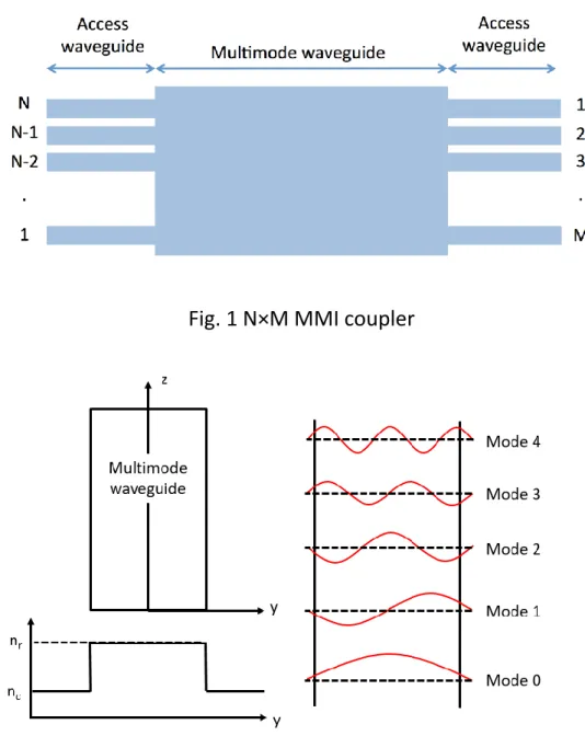
The mode evaluation method is important to investigate the high- speed characteristic of the optical mode device because there is only one output port on the optical mode switch. Moreover, the switching is controlled by injecting the current into the phase shifter, therefore, the fundamental mode and the first mode might be mixed. Thus, the investigation of the mode crosstalk is needed. There are several techniques to distinguish the modes, by using a phase shifter [1], directional coupler [2,3], mode sorting [4], unbalanced Mach-Zehnder interferometer [5], and multimode interference (MMI) coupler [6]. Among these, we choose MMI coupler because it is easy to be integrated with the optical mode switch. There were two kinds of MMI structured that can be separated the modes; 2×2 MMI mode filter and 1×3 MMI mode filter.
Generally, the MMI devices are composed of two parts. One is the center of the multimode waveguide and the access waveguides as shown in Fig. 1. The center multimode waveguide supports a large number of modes, where the MMI occurs. A number of access waveguides are placed for the input ports and output ports. Such devices are generally referred to as N×M MMI couplers, where M and N are the numbers of input and output ports, respectively. Usually, this input and output ports are single mode waveguides for the high-performance MMI devices, however, it could be a few mode
waveguides depends on the application.
Fig. 1 N×M MMI coupler
Fig. 2 Multimode waveguide, refractive index distribution and the supported modes. It shows the multimode waveguide width is WM and the propagating
direction of modes is z-direction.
The 3-D multimode waveguide can be simplified to a 2-D model by effective index method as mentioned above. Fig. 2 shows a step-index multimode waveguide with an effective refractive index nr and a clad index of
modes is z-direction, as shown in Fig. 2 The supported modes number can be calculated by (1a) and (1b). The electric fields distribution of these modes in the multimode waveguide is also shown in Fig. 2. From the mode power distribution, the guided modes penetrated into the cladding can be seen, which is the Goos-Hahnchen shifts.
𝑢 = 𝑚𝜋
2 +1
2𝑡𝑎𝑛−1(𝜔
𝑢) +1
2𝑡𝑎𝑛−1 𝜔1
𝑢 (𝑚 = 0,1,2, … ) (1a) 𝜙 = 𝑚𝜋
2 +1
2𝑡𝑎𝑛−1(𝜔
𝑢) −1
2𝑡𝑎𝑛−1 𝜔1
𝑢 (𝑚 = 0,1,2, … ) (1b) where
{
𝑢 = 𝑘𝛼 𝜔 = 𝜉𝛼 𝜔1 = 𝜎𝛼
(2)
𝑘 = √𝑘02𝑛12− 𝑛12 = 𝑘0√𝑛12− 𝑛eff2 (2a)
𝜎 = √𝛽2− 𝑘02𝑛02 = 𝑘0√𝑛eff2− 𝑛02 (2b)
𝜉 = √𝛽2− 𝑘02𝑛𝑠2 = 𝑘0√𝑛eff2− 𝑛𝑠2 (2c) Where n0, n1, and ns is the refractive index of the coating layer, core, and cladding, respectively, and
𝑡𝑎𝑛(𝑢 + 𝜙) =𝜔
𝑢 (3a)
𝑡𝑎𝑛(𝑢 − 𝜙) =𝜔1
𝑢 (3b)
For a symmetric waveguide, (1) can be written as 𝑢 = 𝑚𝜋
2 + 𝑡𝑎𝑛−1(𝜔
𝑢) (4a) 𝜙 = 𝑚𝜋
2𝑢 (4b)
3.1 2×2 MMI mode filter
Fig. 3. The schematic of 2×2 MMI coupler. An extra Δϕ is needed to make this MMI filter works. The lights will out in TE0A or TE0B depends on the Δϕ
of the input lights.
Fig. 3 shows the 2×2 multimode interference (MMI) coupler, there are two input ports and two output ports. This MMI coupler works as follows:
when the fundamental modes get through the both of input ports with a phase difference of Δϕ=π/2, TE0 input will go through the MMI structure and output from TE0A as a fundamental mode. On the other hands, when the phase difference of Δϕ=3π/2, the fundamental modes get through the MMI
mode gets through the MMI because the first order mode will have a phase difference of π between the input arms.
Fig. 4 The schematic of optical mode switch with 2×2 MMI mode filter. This picture shows that an extra phase shifter is neede to make the MMI mode
filter works.
The merit of this MMI structure is only two output ports needed to distinguish between the fundamental mode and the first order mode.
However, there are two input ports as well, thus, the output port of the mode switching needs to be divided again by Y junction and a phase change region is also needed on one of the input ports to give an extra π/2 phase difference.
This structure will need a complicated fabrication process and evaluation process since another PIN junction is also needed for the MMI mode filter.
Figure 4 shows the schematic mode switching with this 2×2 MMI mode filter.
3.2 1×3 MMI Mode Filter
In order to verify the potential mode crosstalk of the optical mode switch, we fabricated and integrated mode filter with the optical mode switch.
This mode filter was designed based on multimode interference (MMI) coupler [7]. The principle of the MMI device is based on self-imaging as one of the properties of multimode waveguides. For filtering the fundamental mode and first-order mode, we use the simple 1×3 symmetrical rectangular shape of the MMI device that is shown in Fig. 5. The purpose is to distinguish the fundamental mode and first-order mode. It shows that, there is only 1 input port for this MMI mode filter but has 3 output ports. The merit of this MMI mode filter besides there is only one input port, a phase shifter is not needed to distinguish between the fundamental mode and the first mode.
According to this merit, we chose this MMI mode filter configuration to investigate the mode crosstalk of our optical mode switch.
Fig. 5 The schematic of 1×3 MMI coupler. In this mode filter, only one input port is needed and no extra phase shifter is needed to make this mode filter
works.
From self-imaging theory, the first-order mode injected in the center of the MMI propagates as the fundamental mode on both sides of the MMI at 3Lc/4, with Lc as beat length of the two lowest-order modes. On the other hand, the fundamental mode that is injected to the MMI at the center also propagates at the center port as the fundamental mode at 3Lc/4. Therefore, the fundamental mode propagates toward port P1 while the first-order mode will split into two and propagates toward port P21 and P22 as a single-mode.
The BPM simulation result is shown in Fig. 6. Then, the transmittances of each mode are evaluated by monitoring P1, P21, and P22. The mode crosstalk was estimated by using the evaluated transmittances.
Fig. 6 BPM simulation result of Mode filter (a) Fundamental mode and (b) first order mode input. It shows that the fundamental mode will out from
the center output port, while the first-order mode will out from the side output ports.
3.3 Results and discussion
In order to evaluate the 1×3 MMI mode filter, we fabricated three different LMMI 208, 212, and 216 µm with the same WMMI as 10 µm [8]. We fabricate these three different LMMI to get the best mode crosstalk characteristic. The MMI mode filter will be fabricated and integrated with the optical mode switch, thus, the input port of the MMI mode filter should be the same as the input of optical mode switch whose width is 3 µm.
Fig. 7. Evaluated crosstalk from the fundamental mode input. It shows that the best crosstalk was got from the device with the width of 208 µm with
the crosstalk of approximately -20 dB.
Figure 7 shows the result of the evaluated MMI mode filter. The dashed line shows the simulation result of this MMI mode filter as the function of LMMI. The simulation shows that the TE and TM show different results which means this device has a polarization dependency. We also can see that the
best crosstalk was achieved from the LMMI of 208 µm with the crosstalk of approximately -20 dB. From the result, the experimental result is totally different from the simulation result. Moreover, the experimental result looks shifted to the shorter LMMI than the simulation result. This condition happened because of the fabrication error when fabricating the device. The side etching effect was not considered when designing the MMI mode filter. Side etching effect makes the WMMI smaller than 10 µm. The smaller WMMI, the shorter LMMI
needed to get a good crosstalk. Thus, the simulation result also will move to the shorter LMMI. Figure 8 shows the fabricated WMMI, which shows that the WMMI is 0.3 µm smaller than the designed WMMI.
Fig. 8 The fabricated MMI mode filter. It shows the fabrication error of the mode filter, a side etching of 0.3 µm was investigated.
Fig. 9. Shematic of the integrated optical path difference device and 1×3 MMI mode filter.
For comparison purpose, we also fabricated different length variation for the path different device. The length difference is 0 µm, 0.22 µm, 0.26 µm and 0.30 µm that correspond to the refractive index change ΔN of 0, 0.003, 0.004, and 0.005, respectively. We integrated the path difference device with the MMI mode filter to investigate the characteristic of MMI mode filter when the first-order mode is input into the MMI mode filter. Figure 9 shows the schematic of the integrated optical path difference device and the MMI mode filter.
As shown as a solid line in Fig. 10, the cross-state is realized at ΔN = 0.004. This result is matched well with the theoretical results shown as dashed lines in the same figure. The estimated crosstalk was approximately -10 dB for both TE and TM modes at exactly same ΔN. This value is not sufficient for the practical use, however, there is a possibility that the best point may exist at slightly different ∆N of bellow 0.004.
From the Fig. 10, it shows the insertion loss of this device which is approximately 20 dB with the crosstalk of approximately -10 dB. This insertion loss is the collective loss from the coupling loss, loss from the path difference device, and also fr om the MMI mode filter. This condition can be improved by applying the taper into the MMI mode filter as shown in Fig. 11. By the application of such a taper, the MMI coupler performance will be increased [9, 10].
Fig. 10. The Evaluated transmittance as a function of ΔN for TE mode. The dashed line shows the experiment results from the arm’s length different of
0 µm, 0.22 µm, 0.26 µm, and 0.3 µm, while the solid lines shows the simulation results..
The taper is an essential approach to diminish the transition loss between these two dissimilar waveguides of the access waveguide and the multimode waveguide. This dissimilarity makes the modes that propagate inside the MMI changes the phase, thus in some certain length of L inside the MMI differs by 2m, where is m is integer [11]. As the taper width Wt getting closer to the MMI width, then the transition of the access waveguide and the MMI will be smaller. Without taper, the field along the the MMI section diffracts dramatically first and then converges at some L.
Fig. 11. 1×3 MMI mode filter with taper. The taper will make the transition of the access waveguide and the MMI smaller.
Fig. 12. Transmittance simulation of fundamental mode input in 1×3 MMI mode filter with tapper. An improvement of 10 dB at a fabrication error of
0.5 µm can be gotten by using a tapper with the width of 1 µm.
Figure 12 shows the transmittance simulation for the MMI mode filter with the application of the tapers. It shows the transmittance as a function of
transmittance of the fundamental mode when there is no taper in the 1×3 MMI mode filter. The figure also shows that the MMI mode filter error without taper could reach 25 dB/0.5 µm. As already mentioned that the fabrication error of the MMI mode filter was 0.3 µm, the propagation loss from the MMI mode filter itself could reach approximately 15 dB. On the other hand, the application of the taper can improve the MMI mode filter error into only -15 dB/0.5 µm for the width taper of 0.5 µm and -10 dB/0.5 µm for the taper width of 1 µm.
3.4 Conclusions
In this chapter, we first gave a brief explanation of the mode evaluation method that we are using for the MMI mode filter. We were using the 1×3 MMI mode filter because there is only one input port for this MMI mode filter and no phase shifter is needed to make the MMI mode filter working. As a result, MMI mode filter with WMMI of 10 µm and LMMI of 208 µm shows the best mode crosstalk results. By integrating the MMI mode filter, a path difference device was integrated with the MMI mode filter to see the MMI mode filter performance over mode switching device. The result shows that the insertion loss of this device is approximately -20 dB with the crosstalk of approximately -10 dB. This MMI mode filter performance can be increased by applying the taper in the MMI coupler. Simulation result shows that the MMI mode filter with the taper width of 1 µm shows the best result of fabrication
3.5 References
[1] E. Ip, M. Li, K. Bennet, Y. Huang, A. Tanaka, A. Korolev, K. Koreshkov, W.
Wood, E. Mateo, J. Hu and Y. Yano, “146λ×6×19-Gbaud Wavelength- and Mode-Division Multiplexed Transmission over 10×50-km Spans of Few-Mode Fiber with a Gain-Equalized Few-Mode EDFA,” Tech. Dig. OFC, PDP5A.2, 2013 [2] Y. Ding, J. Xu, F. D. Ros, B. Huang, H. Ou and C. Peuchret, “On-chip two- mode division multiplexing using tapered directional coupler-based mode multiplexer and demultiplexer,” Opt. Express, vol. 21, No. 8, pp. 10376-10382, 2014.
[3] T. Uematsu, K. Saitoh, N. Hanzawa, T. Sakamoto, T. Matsui, K. Tsujikawa and M. Koshiba, “Low-loss and broadband PLC-type mode (de)multiplexer for mode-division multiplexing transmission,” Tech. Dig. OFC, OTh1B.5, 2013.
[4] S. Martínez-Garaot, S. Tseng and J. G. Muga, “Compact and high conversion efficiency mode-sorting asymmetric Y junction using shortcuts to adiabaticity,” Opt. Letters, vol. 39, No. 8, pp. 2306-2309, 2014.
[5] W. Y. Chan and H. P. Chan, “Reconfigurable two-mode mux/demux device,” Opt. Express, vol. 22, No. 8, pp. 9282-9290, 2014.
[6] J. Leuthold, R. Hess, J. Eckner, P. A. Besse and H. Melchior, “Spatial mode filters realized with multimode interference couplers,” Opt. Letters, vol.
21, No. 11, pp. 836-838, 1996.