INVITED PAPER
Special Section on Electronic DisplaysFlexible Ultra-Thin Liquid Crystal Devices Using Coat-Debond Polyimide Substrates and Etched Post Spacers
Yuusuke OBONAI†a), Yosei SHIBATA†,Nonmembers, Takahiro ISHINABE†,Member, andHideo FUJIKAKE†,Fellow
SUMMARY We developed flexible LC devices using coat-debond polyimide substrates with a low birefringence and etched post spacers, and clarified that flexible LCDs using post spacers with small spacer distance have a high flexibility without degradation of the image quality. This result ensured the feasibility of flexible LCDs using coat-debond method.
key words: liquid crystal display, flexible display, coat-debond method, polyimide substrate, etched post spacer
1. Introduction
Flexible liquid crystal displays (LCDs) using plastic sub- strates have advantages of thin, light weight, and shock re- sistant. These features are promising for various applica- tions such as rollable large screen televisions and wearable devices[1],[2]. Flexible LCDs also have high reliability be- cause liquid crystalline materials have high stability against oxidation or moisture in the air. Therefore, flexible LCDs can be realized by using plastic substrates with a low gas barrier. For these reason, flexible LCDs have attracted sig- nificant interest as next generation displays. To realize flex- ible LCDs, the plastic substrate is required to have high di- mensional stability against temperature during the fabrica- tion process of the liquid crystal (LC) alignment layer and the thin film transistors[3]. These high temperature pro- cesses have become significant problems because most plas- tic materials have poor thermal stability.
To overcome this issue, a fabrication technique using polyimide (PI) substrates by the coat-debond method was proposed for organic-light-emitting-diode displays[4]–[8].
In this method, ultra-thin PI substrates with a high heat re- sistance are formed on the glass plates. By depositing the PI substrates on the glass plates, the dimensional stability of the PI substrates against temperature can be improved.
After the device fabrication, the glass plates are debonded from the display device. This fabrication process is expected to be suitable for the high-temperature processes mentioned above. However, studies on the application of the coat- debond method for flexible LCDs have been difficult be- cause of the following reasons.
One is that the achromatic transparent PI substrates Manuscript received February 29, 2016.
Manuscript revised June 7, 2016.
†The authors are with Department of Electronics, Graduate School of Engineering, Tohoku University, Sendai-shi, 980–8579 Japan.
a) E-mail: [email protected] DOI: 10.1587/transele.E99.C.1228
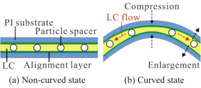
have a high optical birefringence[9],[10]. This optical fea- ture leads to poor contrast ratios and narrow viewing an- gle ranges in flexible LCDs. In a previous study, we have evaluated the phase retardation of PI substrates[11]. How- ever, the influence of the phase retardation of the PI sub- strates on viewing angle range of flexible LCDs has not be- come clear yet. The other challenge is a development of the spacer structure to maintain the thickness of the LC even in a curved state. In the case of particle spacer (see Fig. 1), the thickness of the LC is changed by the flow of LC in a curved state[12]. As a result, the image quality of the LC device is degraded. Alternatively, a post spacer structure fabricated by means of photolithography was proposed[13]. Post spac- ers are fixed on one side of the substrate and can maintain the thickness of the LC in a curved state (see Fig. 2). How- ever, it is considered that flexible PI substrates using the post spacers with large spacer distance make it difficult to main- tain the thickness of the LC because of the deformation of the PI substrates. Therefore, it is necessary to examine the effects of the distance between the post spacers on the image quality of flexible LC devices using PI substrates.
In this study, to investigate the influence of the phase retardation of the PI substrates on viewing angle range, we measured the angular luminance distribution of the PI sub- strates sandwitched between crossed polarizers. In addition, we fabricated flexible LC devices using post spacer struc- tures by varying the spacer distance on the PI substrates, and discussed the effects of the distance between the spacers on
Fig. 1 Flexible LC device using conventional particle spacers.
Fig. 2 Flexible LC device using post spacers.
Copyright c2016 The Institute of Electronics, Information and Communication Engineers
the thickness of the flexible LCDs.
2. Evaluation of the Optical Characteristics of the Polyimide Substrates
We previously clarified that the phase retardation of the thickness direction of our PI substrate is significantly less than that of the ordinary PI substrate by spectroscopic el- lipsometry[11]. It is expected that PI substrate with a low birefringence improve the image quality of flexible LCDs.
In this study, to investigate the influence of the phase retardation of the PI substrates on viewing angle range, we evaluated the optical anisotropy of the PI substrates which have a flexible molecular structure (Polyimide- A) and a rigid molecular structure (Polyimide-B). In or- der to fabricate an ultra-thin PI substrate, we coated the polyamic acid solution on a glass plate by the spin coat- ing method and baked it at 270◦C for two hours un- der a nitrogen atmosphere. We used polyamic acid solu- tion (ECRIOSTM VICT-Bnp, supplied by Mitsui Chem- icals, Inc.) as a Polyimide-A and polyamic acid solution (ECRIOSTM VICT-C, supplied by Mitsui Chemicals, Inc.) as a Polyimide-B. The thickness of PI substrates are 10 µm and the light transmittance of the PI substrate using Polyimide-A is 90% for visible light and the substrate ex- hibits achromatic transparency (see Fig. 3).
To investigate the influence of the phase retardation of the substrates on viewing angle range, we measured the angular luminance distribution in all directions for the PI substrates sandwitched between crossed polarizers using a Conoscope (Autronic-Melchers). Figure 4 shows the angu- lar luminance distribution of the PI substrates sandwitched between crossed polarizers. In the case of the PI substrate using Polyimide-B, light leakage occurred at an oblique viewing angle (see Fig. 4 (b)). In contrast, in the case of the PI substrate using Polyimide-A, the light leakage was signif- icantly less in the wide viewing angle range (see Fig. 4 (a)).
Figure 5 also shows photographs of the PI substrates sand- witched between crossed polarizers. Compared to the PI substrate using Polyimide-B, the light leakage from the PI substrate using Polyimide-A sandwitched between crossed polarizers was significantly less at an oblique viewing an- gle. From these results, it is evident that the PI substrate
Fig. 3 Photograph of the achromatic transparent PI substrate debonded from the glass plate.
using Polyimide-A is suitable for wide viewing angle flexi- ble LCDs.
This result is attributed to the molecular structure of PI. We considered that refractive index of the thickness di- rection of the PI substrate using Polyimide-B became small compared to that of the horizontal direction because the di- rection of the main chain of the Polyimide-B with a rigid molecular structure trended to align in the horizontal direc- tion of the substrate during fabrication process. As a result, the light leakage occurred in the wide viewing angle range because of the large birefringence of the substrate. In con- trast, we considered that in the case of Polyimide-A with a flexible molecular structure, the direction of the main chain of Polyimide-A aligned randomly and the birefringence be- came small.
3. Fabrication of the Flexible LC Devices
To examine the effects of the distance between post spacers on the image quality of the flexible LCDs, we fabricated flexible twisted nematic (TN) mode LC device using the PI substrates of Polyimide-A and post spacers by varying the spacer distance. Figure 6 depicts the fabrication pro- cedure of the flexible LC devices. First, we fabricated the ultra-thin PI substrates on glass plates by the spin-coating method (see Fig. 6 (a)). Next, we coated the negative pho- toresist (PR-200, supplied by Osaka Organic Chemistry In- dustry Ltd.) on the PI substrates (see Fig. 6 (b)), and irra-
Fig. 4 Angular luminance distribution for the PI substrates sandwitched between crossed polarizers.
Fig. 5 PI substrates sandwitched between crossed polarizers (viewing angle: 30◦).
Fig. 6 Fabrication procedure of the flexible LC device using coat-debond PI substrates and post spacers.
Fig. 7 Micrographs of the post spacers fabricated on the PI substrate.
diated UV light through a photomask (see Fig. 6 (c)). Af- ter the photoresist was removed by the photoresist devel- oper except in the exposed area, we baked the post spac- ers at 150◦C for an hour (see Fig. 6 (d)). Subsequently, we coated alignment layer (AL1254, supplied by JSR) on PI substrates and baked at 200◦C for an hour, and conducted rubbing treatment (see Fig. 6 (e)). Then, we applied the seal- ing resin on the PI substrates and laminated the substrates
(see Fig. 6 (f)). After that, we debonded the glass plate from the PI substrate (see Fig. 6 (g)), and injected the LC mate- rial (TD-1016LA, supplied by JNC) by the vacuum injec- tion method (see Fig. 6 (h)). Finally, we debonded the LC devices from the other glass plate (see Fig. 6 (i)).
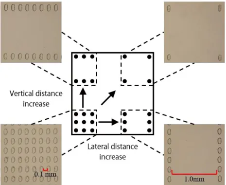
Figure 7 shows micrographs of the post spacers on the PI substrate. The shape of the post spacers is ellipse, and the average size of the post spacers is 100µm in long diameter
and 50µm in short diameter. The height of the post spacers is 4.5µm. We fabricated the post spacers by changing the spacer distance progressively from 0.1 mm to 1.0 mm by 0.1 mm.
4. Observations of the Flexible LC Devices Using Post Spacers
4.1 Effects of the Spacer Distance on the Flexible LC De- vices
Figure 8 shows the photographs of flexible TN mode LC device using post spacer with several distance before and after debonding process. The transmittance of the LC de- vice sandwitched between crossed polarizers was high in all areas before debonding process (see Fig. 8 (a)). However, the transmittance decreased after debonding process with the exception of the area where the spacer distance was less than 0.2 mm (the inside of red dashed lines in Fig. 8). Low transmittance in large spacer distance area is caused by the change in the thickness of the LC during debonding process.
We considered that the LC flow occurred and the thickness of the LC became thin because of the deformation of the PI substrates between the spacers (see Fig. 9). In the case of thin LC thickness, the direction of the polarized light could not rotate enough while the polarized light passed through the LC, and the polarized light was absorbed by output side polarizer. As a result, the transmittance of the LC device decreased in large spacer distance area.
In contrast, in the area where the spacer distance was less than 0.2 mm, we confirmed that the thickness of the LC was maintained constantly and the transmittance did not change during debonding process. In addition, we observed the stripe-like pattern in the area where the spacer distance
Fig. 8 Flexible LC devices using PI substrates and post spacers by varying spacer distance sandwitched between crossed polarizers.
Fig. 9 Deformation of the PI substrates between the post spacers with large spacer distance.
was less than 0.2 mm in one direction, and was more than 0.2mm in another direction. These results indicates that post spacers with the spacer distance below 0.2 mm could main- tain the thickness of the LC, but post spacers with the spacer distance over 0.2 mm could not maintain similarly.
Furthermore, we observed that the LC thickness in the peripheral area of the device was substantially thicker than original LC thickness because the LC flowed into the area during debonding (see Fig. 8 (b)).
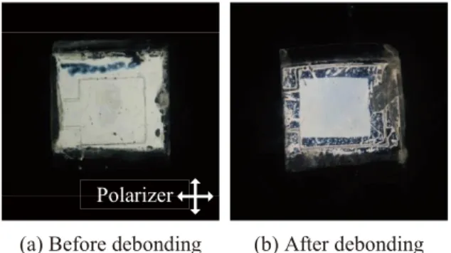
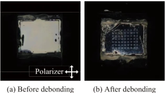
To confirm the validity of above mentioned result, we fabricated two types of flexible LC devices using PI sub- strates and post spacers. The spacer distance was 0.1 mm and 1.0 mm, respectively. In this experiment, we used cross- shaped post spacers to increase contact area of the spacers on the substrate. Figure 10 shows a micrograph of cross- shaped post spacers on the PI substrate.
Figures 11 and 12 show the photographs of flexible TN mode LC devices using cross-shaped post spacer with the spacer distance of 0.1 mm and 1.0 mm, respectively, before and after debonding process. The transmittance of both the LC devices were high before debonding process, however, the transmittance of the LC device using cross-shaped post spacers with the spacer distance of 1.0 mm decreased af- ter debonding process (see Fig. 12). In contrast, in the case of the LC device using post spacers with the spacer dis- tance of 0.1 mm, we observed the thickness of the LC was maintained constantly and the transmittance did not change during debonding process (see Fig. 11). We confirmed that
Fig. 10 Micrograph of cross-shaped post spacers fabricated on the PI substrate (spacer distance: 0.1 mm).
Fig. 11 Flexible LC devices using PI substrates and cross-shaped post spacers (spacer distance: 0.1mm).
Fig. 12 Flexible LC devices using PI substrates and cross-shaped post spacers (spacer distance: 1.0 mm).
Fig. 13 Flexible LC devices in a curved state.
Fig. 14 Flexible LC devices using post spacers with small spacer distance in a curved state.
the post spacers with small spacer distance maintain the LC thickness of flexible LCDs using ultra-thin PI substrates.
4.2 Optical Characteristics of the Flexible LC Devices in a Curved State
Figure 13 (a) shows a photograph of the flexible LC de- vice using cross-shaped post spacers in a curved state. The spacer distance was 0.1 mm. For comparison, we have showed a photograph of the flexible LC device using con- ventional particle spacers in a curved state as shown in Fig. 13 (b). The image quality of the LC device using par- ticle spacers was degraded because the thickness of the LC changes owing to the LC flow in a curved state (see Fig. 1 (b)). In contrast, the image quality of LC device us- ing post spacers with the spacer distance of 0.1 mm was not degraded even in a curved state. This is because the post spacers can maintain the thickness of the LC and suppress the LC flow in the curved state (see Fig. 14). According to the above results, we clarified that flexible LC devices using
ultra-thin PI substrates and post spacers with small spacer distance have a high flexibility without degradation of the optical characteristics.
5. Conclusion
We fabricated achromatic transparent PI substrates with the thickness of 10 µm by the spin coating method, and con- firmed that the phase retardation of the PI substrate with flexible molecular structure is extremely small and the sub- strates are suitable for wide viewing angle flexible LCDs. In addition, we successfully fabricated flexible LC devices us- ing coat-debond PI substrates and etched post spacers. We clarified that flexible LC devices using ultra-thin PI sub- strates and post spacers with small spacer distance have a high flexibility without degradation of the optical charac- teristics even in a curved state. These results ensured the feasibility of fabricating flexible LCDs using ultra-thin PI substrates with a high heat resistance by the coat-debond method.
References
[1] H. Sato, H. Fujikake, H. Fujisaki, S. Suzuki, D. Nakayama, T.
Furukawa, H. Kikuchi, and T. Kurita, “A4-sized liquid crystal dis- plays with flexible light guide plate,” Proc. International Display Workshops, pp.605–608, 2006.
[2] H. Fujikake, H. Sato, T. Murashige, Y. Fujisaki, H. Kikuchi, and T.
Kurita, “Flexible field-sequential-color FLC displays using a bend- able backlight sheet with LED chips,” Proc. International Display Workshops, pp.871–874, 2005.
[3] Z.H. Chen, T.H. Huang, J.K. Lu, and N. Sugiura, “Plastic substrate technology for flexible liquid crystal display,” Proc. International Display Workshops, pp.1461–1464, 2014.
[4] J.-S. Park, T.-W. Kim, D. Stryakhilev, J.-S. Lee, S.-G. An, Y.-S.
Pyo, D.-B. Lee, Y.G. Mo, D.-U. Jin, and H.K. Chung, “Flexible full color organic light-emitting diode display on polyimide plastic substrate driven by amorphous indium gallium zinc oxide thin-film transistors,” Appl. Phys. Lett., vol.95, no.1, 013503, 2009.
[5] C.-C. Lee, Y.-Y. Chang, H.-C. Cheng, J.-C. Ho, and J. Chen, “A novel approach to make flexible active matrix displays,” SID Sym- posium Digest of Technical Papers, vol.41, no.1, pp.810–813, 2010.
[6] J. Jang, M.H. Choi, B.S. Kim, W.G. Lee, and M.J. Seok, “Robust TFT backplane for flexible AMOLED,” SID Symposium Digest of Technical Papers, vol.43, no.1, pp.260–263, 2012.
[7] J. Chen, J.-C. Ho, G. Chen, and C.-C. Lee, “Reliability improve- ment of flexible AMOLED based on auxiliary functional film tech- nology,” SID Symposium Digest of Technical Papers, vol.43, no.1, pp.264–267, 2012.
[8] H. Yamaguchi, T. Ueda, K. Miura, N. Saito, S. Nakano, T. Sakano, K. Sugi, I. Amemiya, M. Hiramatsu, and A. Ishida, “11.7-inch flexible AMOLED display driven by a-IGZO TFTs on plastic sub- strate,” SID Symposium Digest of Technical Papers, vol.43, no.1, pp.1002–1005, 2012.
[9] L. Lin and S.A. Bidstrup, “Processing effects on optical anisotropy in spin-coated polyimide films,” J. Appl. Polym. Sci., vol.49, no.7, pp.1277–1289, 1993.
[10] L. Lin and S.A. Bidstrup, “Effect of molecular orientation on the di- electric properties of spin-coated polyimide films,” J. Appl. Polym.
Sci., vol.54, no.5, pp.553–560, 1994.
[11] Y. Obonai, T. Ishinabe, and H. Fujikake, “Fabrication of flexible ultra-thin liquid crystal devices using coat-debond plastic substrates with etched post spacers,” Proc. International Display Workshops,
pp.191–192, 2015.
[12] H. Sakai, T. Ishinabe, and H. Fujikake, “Flexible polymer-wall- stabilized blue-phase liquid crystal cell using plastic substrates,”
IEICE Trans. Electron., vol.E98-C, no.11, pp.1043–1046, Nov.
2015.
[13] R. Kohno and Y. Iimura, “Study of MVA-LCDs using plastic sub- strates,” Proc. JLCS Japanese Conference of Liquid Crystals, 1b04, 2009.
Yuusuke Obonai received the B.E. degree from Tohoku University, Sendai, Japan, in 2015.
Now, he is a graduate student in the Department of Electronic Engineering, Graduate School of Engineering, Tohoku University. He is engaged in the flexible LCDs using PI substrates. He re- ceived the Outstanding Poster Paper Award from IDW in 2015.
Yosei Shibata has research interests on organic semiconductor devices such as organic transistors and organic photovoltaics. He re- ceived his Ph.D. degree in engineering from Tokyo Institute of Technology (Japan) in March 2013. Then he joined the National Institute of Advanced Industrial Science and Technologies (AIST, Japan) as a postdoctoral position. In Oc- tober 2015, he joined the Department of Elec- tronics of Tohoku University as an Assistant Professor.
Takahiro Ishinabe received his B.S., M.S., and Ph.D. degrees in Electronic Engineering from Tohoku University, Sendai, Japan, in 1995, 1997 and 2000, respectively. From 2000 to 2002, he was a Research Fellow of the Japan Society for the Promotion of Science and from 2003 to 2012, he was an Assistant Professor, and since 2013, he has been an Associate Pro- fessor in the Department of Electronics, Gradu- ate School of Engineering, Tohoku University.
He has also been a Visiting Professor in the CREOL, The College of Optics and Photonics, University of Central Florida from 2010 to 2011. He has been performing a research on ad- vanced liquid crystal displays such as wide viewing angle LCD, reflective full-color LCD, field sequential color LCD and flexible LCD.
Hideo Fujikake received M.E and Ph.D.
degrees from Tohoku University, Japan, in 1985 and 2003, respectively. In 1985, he joined Japan Broadcasting Corporation (NHK). In 1988–
2012, he was with NHK Science and Tech- nology Research Laboratories. Since 2012, he has been a professor at Department of Elec- tronic Engineering, Tohoku University. He re- ceived Best Paper Award from Institute of Elec- tronics, Information and Communication En- gineers (IEICE) in 2001, Best Paper Award from Japanese Liquid Crystal Society (JLCS) in 2001 and 2015, Niwa- Takayanagi Best Paper Awards from Institute of Image Information and Television Engineers of Japan (ITE) in 2003 and 2009, and Electronics So- ciety Award from IEICE in 2013. His current interest is concerned with flexible liquid crystal displays. He also served as a General Vice Chair in International Display Workshops in 2015–2016, a Japan Chapter Chair in IEEE Consumer Electronics Society in 2012–2014, and a Vice President of Japanese Liquid Crystal Society in 2015–2016. He is an IEICE fellow since 2015, and ITE fellow since 2016.