INVITED PAPER
Special Section on Photonic Devices using Nanofabrication Technology and Their ApplicationsEnhancement of Light Emission from Silicon by Utilizing Photonic Nanostructures
Satoshi IWAMOTO†a),Member andYasuhiko ARAKAWA†,Fellow
SUMMARY Efficient silicon-based light sources are expected to be key devices for applications such as optical interconnection. Huge number of researches has been conducted for realizing silicon-based light sources.
Most of them utilized silicon-related materials such as silicon nanostruc- tures or germanium, not crystalline silicon, which has been considered as a poor light emitter because of its indirect electronic bandgap. Light emission properties of materials can be tailored not only by modifying the material properties directly, but also by controlling the electromagnetic environment surrounding the material. Photonic nanostructures are a powerful tool for creating the engineered environment. In this paper, we briefly review the mechanisms for improving the light emission properties of materials by photonic nanostructures and present our recent experimental results show- ing the enhancement of light emission from silicon by introducing photonic crystal structures.
key words: photonic nanostructures, photonic crystals, nanocavity, Purell effect, silicon, light emission, LED
1. Introduction
Recently, silicon photonics technology has attracted much attention as a key technology for implementing optical inter- connection systems in the future electronics [1], [2]. In ad- dition to this widely-recognized target, applications to high- speed communications and to optical sensing have also been discussed [1], [2]. Almost all fundamental optical compo- nents like waveguides and cavities have been investigated and developed. However, the lack of silicon-based efficient light sources limits the potential expansion of its application area. This is because light emission efficiency of bulk crys- talline silicon is extremely low (typically 10−5–10−6) due to the indirect nature of its electronic bandgap.
Many investigations have been conducted for achiev- ing efficient light emission by using silicon-related nanos- tructures such as silicon nanocrystals [3], [4] and silicon ul- trathin films [5], [6], porous silicon [7], and so on. Recently, germanium [8] and its nanostructures [9] also attract the re- searchers. They are promising candidates for light emitters at around 1.5μm. In addition to these approaches based on material engineering, it is possible to utilize photonic nanos- tructures for improving emission properties of silicon and its related materials. Light emission characteristics of materi- als depend both on material parameters such as the transition dipole moment and properties of electromagnetic field sur-
Manuscript received July 4, 2011.
Manuscript revised November 2, 2011.
†The authors are with Institute of Industrial Science and Insti- tute for Nano Quantum Information Electronics, The University of Tokyo, Tokyo, 153-8505 Japan.
a) E-mail: [email protected] DOI: 10.1587/transele.E95.C.206
rounding the material. Photonic nanostructures enable one to tailor the electromagnetic environment, for instance, by strongly confining the light within a small volume, and to control the light emission properties of materials.
One of widely studied photonic nanostrucrtures is pho- tonic crystal (PhC) [10], which has a periodic modulation in refractive index with a periodicity of the order of opti- cal wavelength. This periodicity creates so-called photonic band structures and photonic bandgaps (PBGs). These con- tribute to improve light extraction and light collection effi- ciency due to the diffraction, the change of emission pat- tern, and so on. Furthermore, PhC nanocavity, which is formed by artificially introducing a defect in a PhC lattice, provide an additional opportunity to enhance the light emis- sion. PhC nanocavities have high quality factorQand small mode volumeVc. These unique features pronounce quan- tum nature of light-matter interaction inside the cavity and enhance the light emission rate.
In this paper, we discuss our recent experimental re- sults demonstrating enhanced light emission from crys- talline silicon with PhCs and PhC nanocavities. This pa- per is organized as follows. In Sect. 2, we will briefly re- view how the efficiency of light emission can be improved by photonic nanostructures. In Sect. 3, we present experi- mental results showing enhanced photoluminescence (PL) from crystalline silicon with PhC nanocavities. The effect of cavity size on the enhancement will be also discussed.
Successful transmission of enhanced luminescence from a cavity through a silicon optical waveguide is presented in Sect. 4. In Sect. 5, we will present our recent results on sil- icon light emitting diode with PhC structures. Finally, the summary will be given in Sect. 6.
2. Physics of Enhanced Light Emission Using Photonic Nanostructures
Here, we discuss the total efficiencyηtotalof light emitting devices. ηtotalcan be decomposed into three factors as fol- lows
ηtotal=ηemissionηextractionηcollection, (1) where ηemission is the emission efficiency, which means how much exited carriers can contribute photon radiations, ηextractionis the extraction efficiency of photons from the ma- terial to the outside, andηcollectionis the collection efficiency of extracted photons into the optical setup, only which can be available in applications. In this section, we will briefly Copyright c2012 The Institute of Electronics, Information and Communication Engineers
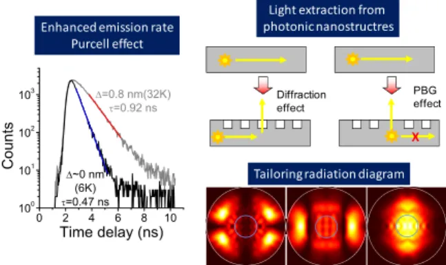
Fig. 1 Possible mechanisms for enhancing light emission from a mate- rial. Left panel shows the change of radiative lifetimeτof a single QD embedded in a PhC nanocavity. Δdenotes the wavelength difference be- tween the QD’s emission peak and the cavity resonance. Right-top panel illustrates the two mechanisms for boosting the extraction of photon from high-index materials. Right-bottom figures show qfar-field radiation pat- tern for several different cavity geometries. Blue circles express the maxi- mum collection angle for a lens with a numerical aperture of 0.42.
summarize the possible mechanisms for improving each fac- tor by utilizing photonic nanostructures.
2.1 Purcell Effect
ηemissionis defined by the ratio of radiative decay rate of ex- cited carriers to total recombination rate, which is the sum of the radiative and non-radiative decay rates. The Fermi’s golden rule tells that the radiative decay rate (spontaneous emission rate in this case) depends not only on material properties but also on the electromagnetic environments. If the light emitter is placed inside an optical cavity, the emis- sion rate to the optical mode is enhanced. This effect is well known as the Purcell effect [11]. The Purcell factor Fp, which indicates the enhancement factor of the emission rate, is usually expressed asFp=(3λ3cQ)/(4π2n3Vc), where λC is the resonant mode wavelength,Qis the quality factor of the mode,n is the refractive index of the material, and Vc is the mode volume. Therefore, PhC nanocavities are promising structures for realizing large enhancement of the radiative emission rate. Figure 1 (left-hand side) shows an example of the change in the emission rate of a single InAs quantum dot (QD) measured at low temperature. When the QD emission wavelength resonates to the cavity mode wavelength, radiative decay time is shortened clearly. In contrast to compound semiconductors, non-radiative recom- bination processes dominate the radiative recombination in crystalline silicon. Therefore, increase of radiative rate di- rectly improves the emission efficiency.
2.2 Diffraction, PBG Effect and Radiation Pattern Modifi- cation
ηextractionandηcollectionare also improved by using photonic nanostructrues. But the mechanisms behind them are based on classical optics not on quantum physics as in the previous subsection. Only a small fraction of photons emitted inside
a high-index material like semiconductors can be extracted and collected due to the total internal reflection between the material and air. PhC structures open the pathways for pho- tons to the outside through the diffraction effects as shown in Fig. 1. If the emission wavelengths are located within the PBG in lateral direction, the light emission only into the vertical direction is allowed. Owing to these mecha- nism, higherηextractioncan be expected from materials with PhC structures than with a flat surface [12]. Besides, radia- tion patterns from photonic nanostructers are largely differ- ent compared with a flat surface. By controlling the cavity geometry, for instance, radiation pattern can be tailored in order to match it with the collection optics (examples are given in Fig. 1). These mechanisms have been utilized in light emitting diodes for improving ηextraction andηcollection
[13]–[15].
3. Enhanced Photoluminescence from Silicon Photonic Crystal Nanocavities
Here, we discuss the enhancement of light emission from crystalline silicon by introducing PhC nanocavities. En- hanced PL has been reported from silicon PhC structures without nanocavities [16], [17]. However, because of the aforementioned mechanism, nanocavities have much poten- tial for improving light emission properties of silicon-based materials.
3.1 Sample Fabrication and Characterization Method PhC nanocavities were fabricated on commercially available silicon-on-insulator (SOI) substrates. The thicknesses of top silicon and buried oxide layers are 200 nm and 1μm, respec- tively. The top silicon layer is lightly p-doped. The resistiv- ity of the layer is ∼20Ωcm. The flow of fabrication pro- cesses is schematically illustrated in Fig. 2. Several types of PhC nanocavities were fabricated by using electron-beam lithography, reactive-ion etching. Finally, air-suspended structures were formed by wet etching using hydrofluoric acid solution. Details for fabrication processes were re- ported in references 18 and 19. We fabricated three different types of cavity structures, H0, H1 and L3 cavities. The H0 cavity [20] was formed by shifting two neighboring air holes oppositely each other along theΓ-K direction of a triangular PhC lattice. The H1 and L3 [21] cavities were formed by removing one and three air holes along the Γ-K direction, respectively. In addition, holes at each edge of the L3 cavity were shifted outward [22]. Scanning electron microscope (SEM) images and distributions of the dominant electric field component for these cavities are shown in Fig. 2. The field distributions are calculated by three-dimensional finite- difference time-domain (3D-FDTD) method [23]. Structural parameters for samples can be found in our previous publi- cations [18], [19].
Samples were characterized by micro PL (μ-PL) setup at room temperature. The pump laser beam was focused onto the sample surface by an objective lens (50×, numer-
Fig. 2 (Left) Fabrication process of Si PhC nanocavities. SEM images for three types of cavities H0, H1, and L3 with shift are shown in right.
Field distributions of the main electric field components (Ey) for cavity modes are also presented.
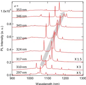
Fig. 3 Room temperature μ-PL spectra from a series of silicon L3 cavities. Samples were excited by a continuou-wave frequency-doubled Nd:YAG laser emitting at 532 nm.
ical aperture = 0.42). PL signals were collected by the same objective lens and were detected by a liquid-nitrogen- cooled InGaAs photodiode array through a single grating monochromator.
3.2 Enhanced PL from L3 Cavities [18]
μ- PL spectra for a series of L3 nanocavities withr/a=0.32, wherer is the radius of air holes anda is the periodicity of PhC lattice, are shown in Fig. 3. Several sharp peaks are clearly observed and peak positions shift towards longer wavelengths as a increases. Peak wavelengths and their polarization dependences show reasonable agreements with
Fig. 4 Comparison between PL spectra from L3 cavities (red curves) and from non-patterned area (blue curves). Spectra from a flat surface are mag- nified by 10 times for easy to see.
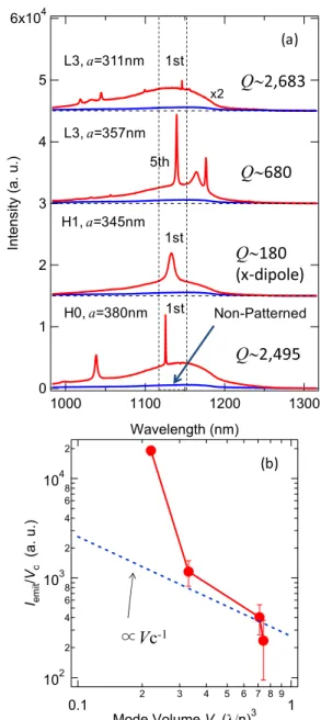
numerical results obtained by 3D-FDTD simulations. The 1st order cavity modes are visible in the spectra with shorter periods. CavityQof the 1st order cavity mode at∼1,150 nm in the spectrum fora=297 nm is estimated at∼5,000 from high-resolution measurements (not shown). This is much smaller than the designedQ(∼21,000). Fabrication imper- fections seem to be the dominant reasons for this degra- dation. Measured Qs for higher order cavity modes are
∼1,000 or less. These are much closer to the designed val- ues.
Large enhancement of PL intensity from PhC nanocav- ities was obtained when higher order cavity modes were tuned at around the peak wavelength of Si PL. Figure 4 com- pares the PL intensity from nanocavities with that from non- patterned areas. PL spectra from non-patterned areas (blue curves) are magnified ten times for better viewing. PhC samples show stronger emission than non-patterned ones over the whole spectral region of silicon PL. From spatially resolved PL measurements, it is confirmed that these en- hanced background emissions mainly come from the PhC areas surrounding the cavities (see Fig. 3 in [18]). The back- ground emission doesn’t resonate with the cavity modes but its spectral range locates inside the PBG of the PhC. Thus, the in-plane PBG effect discussed in Sect. 2.2 is considered as a mechanism for this enhancement. Cavity peak intensi- ties are evaluated by subtracting this background emission.
We define enhancement factors as the ratios of these cavity peak intensities to the PL intensity from the non-patterned area at the corresponding wavelengths. For the sample with r/a=0.37, the enhancement factor reaches up to∼310 for the 5th order cavity mode at 1,191 nm.
This enhancement can be attributed to three mecha- nisms as discussed in Sect. 2. In PhC nanocavities, the ex- traction efficiency is expressed asQmeasured/(2Qv), whereQv is the designed out-of-planeQ. For the 5th mode in Fig. 4, Qmeasured andQv are 447 and 565, respectively. Thus, the extraction efficiency is estimated at∼40%. A 3D FDTD simulation predicts that∼28.5% of extracted photons of the cavity mode can be collected by the objective lens. Totally, for the 5th mode,∼11.3% of emitted photons is collected.
On the other hand, without a PhC pattern, only∼0.2% of emitted photons can be collected in the present experimental setup [24]. Therefore, the enhancement factor due to the in- creased extraction and collection efficiency is approximately 56.5 (11.3%/0.2%). The remaining five times enhancement can be considered as the result of enhanced emission effi- ciency. The Purcell effect is one of possible mechanisms for the enhancement.
Enhancement of silicon light emission using PhC nanocavities was also confirmed by other groups [25], [26].
Temperature dependence of cavity mode emission also indi- cates the contribution of the Purcell effect for the enhance- ment [26].
3.3 Effect of Cavity Mode Volume on PL Enhancement [19]
In order to get more insight for the enhancement of emission efficiency, we investigated the effects of cavity mode volume Vcon light emission.
The expression for the Purcell factorFpin Sect. 2.1 is correct only when the homogeneous linewidth of the emit- ter is much narrower than the linewidth of the cavity mode.
This is the case in which an atom-like emitter, such as a single QD, is used as a light emitter. On the other hand, an emitter like crystalline silicon at room temperature has a broader homogeneous linewidth than that of the cavity mode. A dephasing time shorter than 100 fs has been re- ported for electrons in silicon [27], which corresponds toQ less than 100. In this case,Qin the expression ofFpshould be replaced by the material quality factorQm(=λ/Δλhomo, whereΔλhomois the homogeneous linewidth). Thus, Fp of the resonant mode can be increased by simply reducingVc.
We analyzed room-temperature light emissions from four cavity modes shown in Fig. 2. In Fig. 5(a), spectra for different cavity structures having a mode emission around 1,135 nm, which is close to the peak wavelength of the emis- sion spectrum from a non-patterned area, are shown along with the emission spectrum obtained from the area without a PhC pattern. For the H1 cavity, so-calledx-dipole and y- dipole modes [28] almost overlap each other in this sample.
In the present analysis, we discuss only thex-dipole mode, which can be separated by a polarization-resolved measure- ment. Measured cavity Q’s are also shown in the figure.
These are larger thanQmdetermined by the dephasing time.
Thus,Fpis expected to be mainly determined byQm, not by the cavityQ.
The integrated mode intensity Iobs is estimated after subtracting the background emission as in the previous sub- section.Iobscan be expressed by as follows:
Iobs=ηcollection·ηextraction·Iemit, (2) Iemit=ηmode·P·Ve, (3) whereηcollection and ηextraction are collection and extraction efficiency of photons from silicon slab,Iemitis the emitted mode intensities from the nanocavity,ηmode is the internal
Fig. 5 (a) Room temperatureμ-PL spectra from different types of cavi- ties showing the modes around 1,150 nm. Blue curves are the spectra ob- served from non-patterned regions. Here, a semiconductor laser at 660 nm was used as an excitation light source. (b)Iemit/Vcas a function ofVc. We measured four samples for each cavity mode. The bars on the plot show the ranges ofIemit/Vcfor each mode, while the balls show the average values.
mode emission efficiency per volume,Pis the pump density, andVeis the emitting volume. In the present experiments, Pis constant for all samples.
Figure 5(b) shows a plot of Iemit/Vc as a function of Vc. We calculated designedQ, cavity mode volumeVc, and ηcollection for each mode using 3D-FDTD simulations. Us- ing the simulation results and measured Q’s,ηextraction’s were obtained. Iemit/Vcis considered to be proportional toηmode
because it is reasonable to assume thatVeis approximated by Vc. The electromagnetic fields of the cavity mode are concentrated within the mode volume. It is clearly seen that Iemit/Vc i.e.ηmode increases asVcdecreases. Based on the
simple Purcell theory,ηmode should be proportional toFp, i.e.Vc−1. In contrast, the result shows much stronger depen- dence as shown in Fig. 5(b). This suggests that other mecha- nisms besides the Purcell effect are contributing for the light emission. Effects of phonon localization [29] and carrier lo- calization [17] may be possible mechanisms. In addition, the energy dissipation into other optical modes existing in the emission spectrum such as other cavity modes may be taken into account.
Further investigations are still needed for understand- ing the behavior. However, this result clearly suggests that size of light confinement, instead of cavityQ, is much im- portant for getting larger mode emission from broad emit- ters like crystalline silicon at room temperature. Plasmonic nanocavities will be one of promising structures for this pur- pose. Moreover, this finding offers another option to im- proveηcollectionat the expense of cavity Q. By modulating air-hole size or arrangements around the cavity, radiation diagram from the cavity mode can be tailored so that large parts of photons will be emitted within a narrow angle [30].
4. Detection of Emission from Silicon PhC Nanocavi- ties through a PhC Waveguide[31]
In the previous section, light emission from cavities was monitored above the samples. Here, we present a demon- stration of an in-plane guidance of light generated inside a silicon PhC nanocavity through a lateral PhC waveguide.
This shows a potential of silicon-based internal light sources for optical signal transmission on chips.
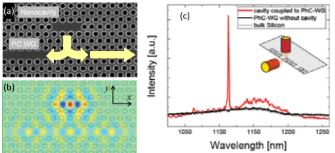
Figure 6(a) shows an SEM image of a device we fab- ricated. A L3 cavity is located close to a PhC waveguide, which is formed by omitting a row of air holes alongΓ-K direction. We chose a distance between the cavity and the waveguide of three rows in order to realize a high coupling efficiency from the cavity to the WG while keeping a moder- ateQ. The coupling efficiency of∼35% and designedQof the order of several thousands are obtained from 3D FDTD simulations.Ey-field distribution at the resonant wavelength of the 1st order cavity mode of the isolated cavity is shown in Fig. 6(b). A clear coupling between the cavity and the
Fig. 6 Propagation of photons emitted from nanocavity through PhC waveguide. (a) SEM image of a L3 cavity coupled with a W1 PhC wave- guide. (b) Field distribution for the wavelength of fundamental cavity mode calculated by 3D FDTD. (c) Measured PL spectrum through the waveguide.
The peak corresponds to the cavity mode.
waveguide is observed.
The signals were detected at the edge of cleaved sam- ple from the lateral side by using a 100x microscope ob- jective controlled by a piezo actuator. The cavity was ex- cited from the top of sample. Here we used a semiconductor laser diode at 405 nm. In Fig. 6(c), we present a typical re- sult. In contrast to the spectrum in Fig. 4, only one peak aroundλ=1,110 nm is observed in the spectrum measured from a PhC waveguide coupled with a L3 nanocavity (red curve). This peak corresponds to the first order cavity mode of the L3 cavity. Higher modes are not visible in this geom- etry. They can’t propagate long distance through the wave- guide because they don’t cross the waveguide mode under the light-line in this particular sample. The detected sig- nal intensity strongly depends on the position of objective lens. When the objective moves in vertical and lateral di- rections, the detected signal quickly decreased. This also proves that signals were detected through the waveguide.
We estimate the propagation length, which is defined as a length where the initial intensity decays by 3 dB by calculat- ing the absorption coefficient using the formula in [32]. The absorption length ranges 5–50 cm for the wavelength region of 1,150–1,200 nm by taking into account the reduction of group velocity in PhC waveguide compared to bulk silicon.
Thus, relatively long propagation of light from internal light sources can be achieved by tuning the cavity wavelength.
5. Demonstration of Silicon Light Emitting Diode with Photonic Crystal Structures[33]
Highly-efficient silicon-based light emitting diode (LED) is one of important targets of research. Only a few researches have been reported on the development of silicon LEDs so far. Using very high-quality crystalline silicon, a Si LED with surprisingly high efficiency (∼1%) have been demon- strated [34]. A silicon LED with a planar microcavity have been fabricated. However it showed only∼2 times enhance- ment of electro-luminescence (EL) [35]. Our aim is to uti- lize PhC nanocavities for realizing efficient silicon-based LED. As the first step, we have fabricated a silicon LED with a PhC pattern without nanocavities and have demon- strated large enhancement of EL compared with a SOI LED with a flat surface.
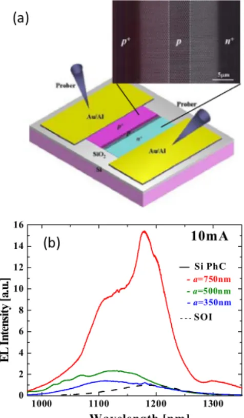
Our device structure is schematically depicted in Fig. 7(a). A SEM image of the central area of the device is also shown. Silicon PhC LEDs were fabricated on com- mercially available SOI substrates. Lateral p+-p-n+ struc- tures were formed by utilizing selective-area ion implanta- tion technique. The length ofi-region is 5μm. The buried oxide layer was not removed in this experiment. I-V traces showed clear rectification behavior with a turn-on voltage about 0.8 V, which is a typical value for silicon diodes. The series resistance becomes bigger when a PhC structure is patterned. The change in resistivity can be well explained by considering the reduction of the cross section due to the introduction of air holes.
EL spectra for devices with different PhC periodicities
Fig. 7 (a) Schematic illustration of silicon PhC LED. SEM for the central part of device is also shown. (b) EL spectra from PhC LEDs with differ- ent periodicities and from a SOI LED with flat surface. All spectra were measured under the injected current of 10 mA and at room temperature.
at an injected current of 10 mW are shown in Fig. 7(b). For comparison, EL spectrum from a SOI LED with a flat sur- face is also shown. It is clear that EL intensity becomes strong by introducing PhC patterns. Particularly, peak inten- sity from the LED with a PhC period of 750 nm is more than 10 times stronger than from a LED with flat surface. Inte- grated intensity of the PhC-LED is enhanced by 14 times compared with a non-patterned LED. Numerical simula- tions indicate that these enhancements are mainly attributed to the improved extraction and collection efficiencies due to the photonic band structures. We also observed much larger enhancement (∼140 times) of peak and integrated intensities when the buried oxide layer underneath the PhC pattern is removed. Details will be reported elsewhere.
6. Conclusion
In this paper, we briefly discussed the mechanisms for im- proving the light emission properties of materials by utiliz- ing photonic nanostructures and presented our recent exper- imental works on light emission from silicon with PhCs and PhC nanocavities. There are still plenty of rooms of basic researches in order to clarify the detail mechanisms for the enhancement of emission efficiency. However, our exper- imental results show that photonic nanostructures are use- ful for controlling light emission from silicon. Note that photonic nanostructures are also effective for enhancing the light emission from germanium [36], which has received
much attention since the first report of the optically pumped laser [37]. Moreover, combinations with engineered materi- als such as germanium QDs will expand the possibilities of group-IV based light sources. Germanium QDs have been already embedded in optical micro cavities and enhanced luminescence has been reported [38].
There are big hurdles to be crossed before reaching the goal, realization of efficient silicon-based light sources. We believe, however, photonic nanostructures will play crucial rolls on the development of these devices.
Acknowledgments
We thank S. Nakayama and S. Ishida of the University of Tokyo, and A. Gomyo of NEC corporation for the exper- iments on the fabrication and on the characterization. We also thank Y. Ota of the University of Tokyo for the fruitful discussions. The works discussed here were supported by Japan Society for the Promotion of Science (JSPS) through its “Funding Program for World-Leading Innovation R&D on Science and Technology (FIRST Program)”, the Special Coordination Founds for Promoting Science and Technol- ogy, and Kakenhi 216860312, MEXT, Japan.
References
[1] L. Pavesi and D.J. Locjwood, ed., Silicon Photonics, Springer, Berlin, 2004.
[2] G.T. Reed, ed., Silicon Photonics: The state of the art, John Wiley
& Sons, Chichester, 2008.
[3] L. Pavesi, L. Dal Negro, C. Mazzoleni, G. Franzo, and F. Priolo,
“Optical gain in silicon nanocrystals,” Nature, vol.408, pp.440–444, 2000.
[4] R.J. Walters, G.I. Bourianoff, and H.A. Atwater, “Field-effect elec- troluminescence in silicon nanocrystals,” Nat. Matt., vol.4, pp.143–
146, 2005.
[5] S. Saito, D. Hisamoto, H. Shimizu, H. Hamamura. R. Tsuchiya, Y. Matsui, T. Mine, T. Arai, N. Sugii, K. Torii, S. Kimura, and T.
Onai, “Silicon light-emitting transistor for on-chip optical intercon- nection,” Appl. Phys. Lett., vol.89, no.16, 163504, 2006.
[6] S. Saito, Y. Suwa, H. Arimoto, N. Sakuma, D. Hisamoto, H.
Uchiyama, J. Yamamoto, T. Sakamizu, T. Mine, S. Kimura, T.
Sugawara, and M. Aoki, “Stimulated emission of near-infrared ra- diation by current injection into silicon (100) quantum well,” Appl.
Phys. Lett., vol.95, no.24, 241101, 2009.
[7] Y. Kanemitsu, “Light emission from porous silicon and related ma- terials,” Phys. Rep., vol.263, no.1, pp.1–91, 2000.
[8] X. Sun, J. Liu, L.C. Kimerling, and J. Michel, “Direct gap photolu- minescence of n-type tensile-strained Ge-on-Si,” Appl. Phys. Lett., vol.95, no.1, 011911, 2010.
[9] W.-H. Chang, A.T. Chou, W.Y. Chen, H.S. Chang, T.M. Hsu, Z.
Pei, P.S. Chen, S.W. Lee, L.S. Lai, S.C. Lu, and M.-J. Tsai, “Room- temperature electroluminescence at 1.3 and 1.5μm from Ge/Si self- assembled quantum dots,” Appl. Phys. Lett., vol.83, no.14, 2958, 2003.
[10] J.D. Joannopoulos, R.D. Meade, and J.N. Winn, Photoni Crystals, Princeton University Press, Princeton, 1995.
[11] E.M. Purcell, “Spontaneous emission probabilities at radio frequen- cies,” Phys. Rev., vol.69, p.681, 1946.
[12] S. Fan, P.R. Villeneuve, and J.D. Joannopoulos, “High extraction efficiency of spontaneous emission from slabs of photonic crystals,”
Phys. Rev. Lett., vol.78, no.17, pp.3294–3297, 1997.
[13] H.-Y. Ryu, J.-K. Hwang, Y.-J. Lee, and Y.-H. Lee, “Enhancement of
light extraction from two-dimensional photonic crystal slab struc- tures,” IEEE J. Sel. Top. Quantum Electron., vol.8, no.2, pp.231–
237, 2002.
[14] Y.R. Do, Y.C. Kim, Y.-W. Song, C.-O. Cho, H. Jeon, Y.-J. Lee, S.-H.
Kim, and Y.-H. Lee, “Enhanced light extraction from organic Light- Emitting diodes with 2D SiO2/SiNxphotonic crystals,” Adv. Matt., vol.15, no.14, pp.1214–1218, 2003.
[15] J.J. Wierer, Jr., A. David, and M.M. Megens, “III-nitride photonic- crystal light-emitting diodes with high extraction efficiency,” Nat.
Photo., vol.3, pp.163–169, 2009.
[16] B. Cluzel, N. Pauc, V. Calvo, T. Charvolin, and E. Hadji, “Nanobox array for silicon-on-insulator luminescence enhancement at room temperature,” Appl. Phys. Lett., vol.88, no.13, 133120, 2006.
[17] B. Cluzel, V. Calvo, T. Charvolin, E. Picard, P. Noe, and E. Hadji,
“Single-mode room-temperature emission with a silicon rod lattice,”
Appl. Phys. Lett., vol.89, no.20, 201111, 2006.
[18] S. Iwamoto, Y. Arakawa, and A. Gomyo, “Observation of enhanced photoluminescence from silicon photonic crystal nanocavity at room temperature,” Appl. Phys. Lett., vol.91, 211104, 2007.
[19] S. Nakayama, S. Ishida, S. Iwamoto, and Y. Arakawa, “Effect of cav- ity mode volume on photoluminescence from silicon photonic crys- tal nanocavities,” Appl. Phys. Lett., vol.98, no.17, 171102, 2011.
[20] Z. Zhang and M. Qiu, “Small-volume waveguide-section high Q microcavities in 2D photonic crystal slabs,” Opt. Express, vol.12, no.17, p.3988, 2004.
[21] Y. Akahane, T. Asano, B.-S. Song, and S. Noda, “Investigation of high-Q channel drop filters using donor-type defects in two- dimensional photonic crystal slabs,” Appl. Phys. Lett., vol.83, no.8, p.1512, 2003.
[22] Y. Akahane, T. Asano, B.-S. Song, and S. Noda, “High-Q photonic nanocavity in a two-dimensional photonic crystal,” Nature, vol.425, p.944, 2003.
[23] A. Taflov and S.C. Hagness, ed., Computational Electrosynamics:
The Finite-Difference Time-Domain Method, Artech House, New York, 2000.
[24] M. Zelsmann, E. Picard, T. Charvolin, E. Hadji, M. Heitzmann, B.
Dalzotto, M.E. Nier, C. Seassal, P. Rojo-Romeo, and X. Letartre,
“Seventy-fold enhancement of light extraction from a defectless photonic crystal made on silicon-on-insulator,” Appl. Phys. Lett., vol.83, no.13, 2542, 2003.
[25] M. Fujita, Y. Tanaka, and S. Noda, “Light emission from silicon in photonic crystal nanocavity,” IEEE J. Sel. Top. Quantum Electron., vol.14, no.4, p.1090, 2008.
[26] N. Hauke, T. Zabel, K. Muller, M. Kaniber, A. Laucht, D. Bougeard, G. Abstreiter, J.J. Finley, and Y. Arakawa, “Enhanced photolumi- nescence emission from two-dimensional silicon photonic crystal nanocavities,” New J. Phys., vol.12, no.5, 053005, 2010.
[27] T. Sjodin, C.-M. Li, H. Petek, and H.-L. Dai, “Ultrafast transient grating scattering studies of carrier dynamics at a silicon surface,”
Chem. Phys., vol.251, no.1-3, 205, 2000.
[28] O. Painter, J. Vuckovic, and A. Scherer, “Defect modes of a two- dimensional photonic crystal in an optically thin dielectric slab,” J.
Opt. Soc. Am. B, vol.16, no.2, 275, 1999.
[29] S.G. Cloutier, C.-H. Hsu, P.A. Kossyrev, and J. Xu, “Enhancement of radiative recombination in silicon via phonon localization and selection-rule breaking,” Adv. Matter., vol.18, no.7, p.841, 2006.
[30] N. Tran, S. Combrie, P. Colman, A.D. Rossi, and T. Mei, “Verti- cal high emission in photonic crystal nanocavities by band-folding design,” Phys. Rev. B, vol.82, no.7, 075120, 2010.
[31] D.F. Dorfner, S. Iwamoto, M. Nomura, S. Nakayama, J.J. Finley, G. Abstreiter, and Y. Arakawa, “Outcoupling of light generated in a monolithic silicon photonic crystal nanocavity through a lateral waveguide,” Jpn. J. Appl. Phys., vol.48, no.6, 062003, 2009.
[32] R.A. Falk, “Near IR absorption in heavily doped silicon — An em- pirical approach,” Int. Symp. Testing and Failure Analysis, 2000.
[33] S. Nakayama, S. Iwamoto, S. Ishida, and Y. Arakawa, “Demonstra- tion of a silicon photonic crystal slab LED with efficient electrolu-
minescence,” 2010 International Conference on Solid State Devices and Materials, Japan, D-4-3, Sept. 2010.
[34] M.A. Green, J. Zhao, A. Wang, P.J. Reece, and M. Gal, “Efficient silicon light-emitting diodes,” Nature, vol.412, 805, 2001.
[35] J. Potfajova, B. Schmidt, M. Helm, T. Gemming, M. Benyoucef, A. Rastelli, and O.G. Schmidt, “Microcavity enhanced silicon light emitting pn-diode,” Appl. Phys. Lett., vol.96, no.15, 151113, 2010.
[36] S. Nakayama, S. Iwamoto, S. Ishida, D. Bordel, E. Augendre, L.
Clavelier, and Y. Arakawa, “Enhancement of photoluminescence from germanium by utilizing air-bridge-type photoni crystal slab,”
Physica E, vol.42, no.10, pp.2556–2559, 2010.
[37] J. Liu, X. Sun, R. Camacho-Aguilera, L.C. Kimerling, and J. Michel,
“Ge-on-Si laser operating at room temperature,” Opt. Lett., vol.35, no.5, pp.679–681, 2010.
[38] J. Xia, Y. Takeda, N. Usami, T. Maruizumi, and Y. Shiraki, “Room- temperature electroluminescence from Si microdisks with Ge quan- tum dots,” Opt. Express, vol.18, no.13, p.13945, 2010.
Satoshi Iwamoto received B.S. and M.S., and Ph.D. degrees in the applied physics from the University of Tokyo, Japan, in 1997, 1999, 2002, respectively. From 2002, he has joined Institute of Industrial Science, the University of Tokyo, as a Research Associate, and started the research on photonic nanostructures and light- matte interactions in these structures. He was promoted to a Lecturer and an Associated Pro- fessor in 2003 and 2007, respectively. Since 2006, he has been investigating light emission properties of group IV materials with photonic nanostructures.
Yasuhiko Arakawa received his B.S. de- gree from The University of Tokyo and his M.S.
and Ph.D. degrees from The University of To- kyo in 1975, 1977 and 1980, respectively, all in Electrical Engineering. He joined the Univer- sity of Tokyo as an Assistant Professor in 1980, and was appointed as a Full Professor in 1993.
He is currently the Director of Institute for Nano Quantum Information Electronics (NanoQuine) and a Professor at Institute of Industrial Science, the University of Tokyo. He is a technical advi- sor of QD Laser Inc. He is a member of Science Council of Japan, Vice President of ICO, IEEE Fellow, OSA Fellow, JSAP Fellow, and IEICE Fel- low, respectively. His research interest has been in the area of physics, and growth for quantum dot-based new light sources such as quantum dot lasers, single photon emitters and entangled photon generators. He has au- thored 490 papers in leading technical journals and has given more than 200 invited presentations at international conferences. He has received many awards including IBM Science Award (91), Nissan Science Award (92), Quantum Device Award (02), IEEE/LEOS William Streifer Award (04), Leo Esaki Prize (04), Wall Street Journal Technology Innovation Award (05), Fujiwara Prize (07), Prime Minister Award (07), IEEE David Sarnoff Award (09), Medal with Purple Ribbon (09), Minister of Economy, Trade and Industry Award (10), C & C Prize (10), OSA Nick Holonyak Award (11), and Heinrich Welker Award (11).