INVITED PAPER
Special Section on Leading-Edge Technology of Superconductor Large-Scale Integrated CircuitsCircuit Description and Design Flow of Superconducting SFQ Logic Circuits
Kazuyoshi TAKAGI†,††a), Nobutaka KITO†††,††,Members,andNaofumi TAKAGI†,††,Senior Member
SUMMARY Superconducting Single-Flux-Quantum (SFQ) devices have been paid much attention as alternative devices for digital circuits, because of their high switching speed and low power consumption. For large-scale circuit design, the role of computer-aided design environment is significant. As the characteristics of the SFQ devices are different from conventional devices, a new design environment is required. In this paper, we propose a new timing-aware circuit description method which can be used for SFQ circuit design. Based on the description and the dedicated algorithms we have been developing for SFQ logic circuit design, we pro- pose an integrated design flow for SFQ logic circuits. We have designed a circuit using our developed design tools along with the design flow and demonstrated the correct operation.
key words: single-flux-quantum circuit, design methodology, circuit de- scription, logic design, layout design, design verification
1. Introduction
Superconducting Single-Flux-Quantum (SFQ) devices are expected to be emerging digital circuit devices that can fol- low conventional CMOS devices [1]. With the progress of integration and the development of technologies of high- speed interconnecting transmission lines [2], SFQ digital circuits with thousands of Josephson junctions working at high clock frequency up to several tens of GHz have become feasible [3]–[5].
To design large-scale circuits, computer-aided circuit design systems are indispensable. For CMOS circuits, sys- tems to support various aspects of the design process have been used for years. Though some part of the software tools can be applied to SFQ circuit design, dedicated design al- gorithms and tools are needed in many stages in the design process, because the nature of SFQ circuits is different from that of CMOS circuits.
In SFQ circuits, digital information is represented by a magnetic flux quantum passing through a superconduct- ing loop and is transmitted by a voltage pulse generated by a Josephson junction. From the viewpoint of logic design, SFQ circuits operate by pulse logic and hence have different circuit structure compared to conventional level logic. Pa- rameters to consider in optimization, such as trade-offvalues between timing and area costs and balances between logic
Manuscript received August 2, 2013.
Manuscript revised November 12, 2013.
†The authors are with the Graduate School of Informatics, Kyoto University, Kyoto-shi, 606-8501 Japan.
††The authors are with ALCA-JST.
†††The author is with the School of Engineering, Chukyo Uni- versity, Toyota-shi, 470-0393 Japan.
a) E-mail: [email protected] DOI: 10.1587/transele.E97.C.149
gate and transmission performances, are also special in SFQ circuit design. Design flow for high-performance SFQ cir- cuits should take these factors into account.
Design tools for SFQ circuits have been developed and an integrated design methodology has been proposed in [6].
In their work, circuits are designed with zero-skew syn- chronous clocking, which is common in semiconductor cir- cuits. They successfully showed that design automation of large-scale SFQ circuits is possible with synchronous clock- ing scheme.
Our aim is to develop an advanced design methodol- ogy applicable to SFQ circuits with flow-clocking, which is a skewed clocking scheme suitable for high-speed SFQ circuits. Here, new algorithms to deal with the distinctive timing-related issues are required.
Design environment and tools for flow-clocking SFQ circuits have to be concious of signal timing at each gate.
To specify the logical behavior of an SFQ circuit in a con- ventional design environment, a circuit description close to physical layout is required, because the signal timing affects the functionality. However, close relationship between log- ical and phisical design stages results in difficulties in the design flow. To resolve the situation, in this paper, we pro- pose a timing-aware circuit description method in logical schematic level. By using the proposed description, signal timing which affects the circuit behavior can be specified completely, while being independent of physical design.
Based on the timing-aware description and the dedi- cated algorithms we have been developing for SFQ logic circuit design, we propose a design flow for SFQ logic cir- cuits. For given circuit description in logic level, synthesis, placement, and routing processes are performed to obtain a circuit layout. At each stage, SFQ-specific design algo- rithms are employed. To deal with the pulse-based behav- ior, we have to construct a mechanism for synchronization.
Because of the high-speed switching, timing design should take priority over other parameters at every stage. The pro- posed design flow is composed of these stages combined consistently.
This paper is organized as follows. We show the is- sues to consider in designing SFQ logic circuits in Sect. 2.
In Sect. 3, we propose a timing-aware circuit description and show a circuit simulation method as an application of the de- scription. In Sect. 4, we describe the proposed design flow for SFQ circuits. An overview of the individual algorithms and an example of circuit design to demonstrate the prac- ticality of the design flow are also shown. Section 5 is a Copyright c2014 The Institute of Electronics, Information and Communication Engineers
conclusion.
2. Design issues of SFQ Logic Circuits
2.1 Logical Expression and Timing
The main reason that we need new circuit description method and new design algorithms for SFQ logic circuits is that they work by pulse logic. In designing SFQ logic cir- cuits, presence and absence of a pulse are associated with logic values ‘1’ and ‘0’ respectively. A clock signal is in- troduced to define time frames and the logic value ‘0’ is distinguished from the state that the pulse has not arrived.
Therefore, we have to be aware of the timing of clock distri- bution. Because timing information has not been described in a circuit schematic, a new timing-aware circuit descrip- tion method is necessary. New design algorithms for timing- driven optimization are also required.
Each SFQ logic gate is driven by synchronous clock pulses, and the circuit behavior can be interpreted in the same way as conventional CMOS logic circuits. However, it is not practical to design totally synchronous circuits in which a clock pulse is fed to all gates at the same time, because the switching speed is very high and wiring delay is not negligible. Therefore, flow-clocking design is com- monly used, where clock skew for each logic gate is intro- duced. A clock pulse is distributed along with the data and reaches to each gate after a different amount of time. Hence, the clock is skewed, i.e., the time frames defined at each gate are different to one another. For correct operation, we have to design the topology and the geometry to distribute a clock signal carefully, in order to ensure that setup and hold con- ditions at each gate are satisfied.
Flow-clocking can be classified into several schemes.
In the concurrent-flow clocking scheme, clock pulses are fed to the circuit along with data pulses, and a clock pulse arrives before the data pulses at each gate. A circuit with concurrent-flow clocking operates in a pipelined manner where each level of gates corresponds to a stage. In the clock-follow-data clocking scheme, clock pulses are fed to the circuit along with data pulses, which is the same as the concurrent-flow clocking, but a clock pulse arrives after the data pulses at each gate. Behavior of a clock-follow-data clocking circuit is interpreted in the same way as a combi- national circuit.
Because SFQ circuits can operate at high switching fre- quency, timing-related issues are critical throughout the de- sign flow. In typical circuit design, concurrent-flow clocking is employed as a whole, and a small cluster of gates is pos- sibly designed by the clock-follow-data clocking scheme to save operation clock cycles. If the clock timing of the fabri- cated circuit is not as intended by the designer, the circuit does not work correctly. Therefore, timing-aware circuit description is required to specify the logical behavior com- pletely. Because timing adjustment in detailed design on trial-and-error basis is hard for large-scale circuits, design automation using computer-aided design tools is indispens-
able.
2.2 Cell-Based Design and Interconnects
Design of SFQ logic circuits is performed in a cell-based manner [7]. The set of logic gates are predefined as a cell li- brary, which contains logical and physical information. Cir- cuits are implemented by arranging cells and interconnects.
Connections between cells are implemented by simply plac- ing next to each other, or by using Josephson transmission lines (JTLs) and splitters. Splitters and JTLs are also prede- fined in the cell library. With the progress of the fabrication process technology, passive transmission lines (PTLs) have become available as interconnects.
There are several aspects specific to SFQ devices to consider in circuit design. The timing requirement is much more severe compared to conventional CMOS circuits, be- cause of the high switching speed and the pulse-based be- havior. As for the circuit topology, we have to use active cells to make fan-out, because PTLs are basically one-to- one transmission lines. In timing design, though PTLs can be used for faster interconnects especially for long connec- tions, they require overheads of transmitters and receivers.
In layout design, JTLs have to be arranged in the active layer, while PTLs are routed through other layers.
In the design process for SFQ circuits, there have been a lot of procedures processed manually, and our aim is to establish an automated design flow. Computer-aided design algorithms should be designed with the SFQ-specific issues taken into account.
3. Timing-Aware Circuit Description and Simulation
3.1 Timing-Aware Circuit Description
SFQ circuits of the same topology may have different func- tions, depending on the signal timing caused by switching and transmission delay. However, transmission delay is not usually specified in the circuit schematic. Therefore, circuit schematic solely cannot describe the functionality of the cir- cuits and we have to be aware of temporal information. In conventional design environment, the logical behavior of the SFQ circuits cannot be settled before detailed layout design.
Therefore, logical and physical design of SFQ circuits are tightly bounded together, which is a bad practice with re- spect to step-wise refinement of design.
To cope with this situation, we propose a timing-aware schematic representation of SFQ circuits [8]. Because the function of each gate in a circuit depends on the timing of pulse arrivals, we attach an annotation of the order of pulse arrivals to each gate in a schematic to describe function ac- curately. The order is represented by inequalities between input terminals including the clock input. We define peri- odical time frames, which are typically the clock cycles, to define the order.
Here, we consider circuits which satisfy the following conditions.
Condition 1: Each gate in a circuit has the order of possible pulse arrivals independent of parameters such as clock frequency and gate delay.
Condition 2: The order of possible pulse arrivals at each gate is always consistent with a partial order defined on the input terminals.
By these conditions, we exclude circuits containing multi- cycle paths and autonomous oscillator circuits.
The following proposition is derived from the above conditions and now we can specify the function of an SFQ circuit accurately.
Proposition 1: The function of an SFQ circuit is specified uniquely by the schematic with annotations of the order of pulse arrivals.
Proof: When input pulses are fed to a circuit, internal states of the gates after current time frame are determined by the current internal states and the current input pulses, indepen- dent of the clock frequency (Condition 1). The order of pulse arrivals at each gate is specified by the annotation and hence the behavior of the gate is completely described (Con- dition 2). Therefore, the function of the circuit as a whole is
specified uniquely.
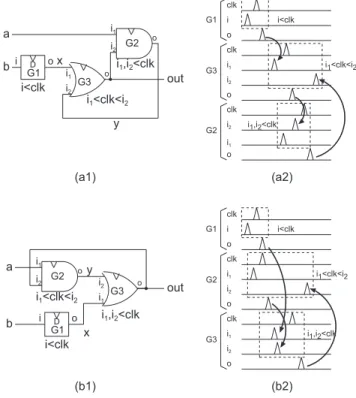
Figures 1(a) and (b) are examples of schematics with annotations. Figure 1(a) is a circuit with clock-follow- data clocking and Fig. 1(b) is a circuit with concurrent- flow clocking. In a circuit with clock-follow-data clocking, data pulses arrive at each gate before a clock pulse arrives.
Therefore, we give an inequality “i1,i2<clk” for each gate in Fig. 1(a). In a circuit with concurrent-flow clocking, a clock pulse arrives at each gate before data pulses arrive.
Therefore, we give an inequality “clk <i1,i2” for each gate in Fig. 1(b).
Figures 2(a1) and (b1) are examples of SFQ circuit schematics with feedback loops. Clock wires are omitted in these figures. Figures 2(a2) and (b2) show the behav- ior of the circuits in Figs. 2(a1) and (b1), respectively. In Fig. 2(a1), gateG3 receives a pulse from the feedback loop.
The pulse through the loop arrives atG3 after a clock pulse arrives, and the logical value is interpreted in the next time frame. In Fig. 2(b1), G2 receives a pulse from the feed- back loop. Though the circuits shown in Figs. 2(a1) and (b1) work differently, they cannot be distinguished by the schematic descriptions only, because they have the same topology. Annotations of the order of pulse arrivals are suf- ficient to specify the circuit behavior.
Fig. 1 SFQ logic circuit schematics with annotations of the order of pulse arrivals. (a) Clock-follow-data clocking. (b) Concurrent-flow clock- ing.
Now we show a formulation for describing the anno- tations of the order of pulse arrivals in circuit description language for SFQ circuits. This description can be used for design automation for SFQ logic circuits. In the new de- scription language, we represent a gate as follows.
o=GAT E G(w1@p1, w2@p2, . . . , wk@pk);
Here,GAT Eis a primitive logic function, such as AND, OR and XOR.Gis the instance name of the gate.w1, w2, . . . , wk
are inputs of the gate. p1,p2, . . . ,pkare integers to describe the order of pulse arrivals. ois the output of the gate. This description represents a sequence of inequalities for each gate by the values ofp1,p2, . . . ,pk. pi<pjmeans the order that the pulse onwiprecedes the pulse onwj.
A description of a logic circuit is a collection of the descriptions of all gates. Any SFQ circuit satisfying Condi- tions 1 and 2 can be described. For example, we describe the circuit in Fig. 1(a) as follows.
d =AND G1(a@1,b@1,clk@2);
e=AND G2(c@1,d@1,clk@2);
Because a clock pulse arrives after data inputs, the value attached to “clk” is greater than those for “a”, “b”, “c”, and
“d”. The same value 1 for “a” and “b”, and “c” and “d”
means that we give no order between these inputs. Another example is in Fig. 3, which corresponds to the circuit with a
Fig. 2 Examples of SFQ logic circuits with feedback loops.
1: x = D G1( b@0, clk@1 );
2: out = OR G3( x@0, y@2, clk@1 );
3: y = AND G2( a@0, out@0, clk@1 );
Fig. 3 Circuit description for Fig. 2(a1).
1: //Input: circuit description(composed ofNgates fromG1toGN), 2: // input sequenceI0,I1,. . .(each for inputikat time frames 1 toT) 3: //Output: output sequence
4: //
5: //Definition ofGl: ol=gatel Gl(wl,1@pl,1, wl,2@pl,2, . . . , wl,kl@pl,kl);
6: //pclkl : the order for “clk” input ofGlif it exists, otherwise∞. 7: //PHl: set of pairs of input and order{wl,k@pl,k|pl,k>pclkl }. 8: //PLl: set of pairs of input and order{wl,k@pl,k|pl,k≤pclkl }. 9: //olcorresponds to sequenceOl.
10: //wl,1, . . . , wl,klcorrespond to sequencesWl,1, . . . ,Wl,kl, respectively.
11:
12: Prepare sequences of lengthT corresponding to wires in the description.
13: Initialize all sequences except input sequences (Invalidate all elements of sequences).
14:
15: fortfrom 1 toT do 16: S← {1,2, . . . ,N} 17: whileSis not emptydo
18: SelectlfromSsuch that all sequences corresponds toPLlhave validt-th elements.
19: RemovelfromS.
20: Calculate new internal state ofGlusing (t−1)-th elements of sequences corresponding toPHlaccording to the order.
21: Calculate new internal state ofGlusingt-th elements of sequences corresponding toPLlaccording to the order.
22: Ol[t]←output ofGl. 23: end while
24: end for
25: printoutput sequences
Fig. 4 Logic simulation algorithm.
feedback loop in Fig. 2(a1).
3.2 Circuit Simulation in Logic Level
The logical behavior of a circuit is completely specified with the proposed schematic level description. One of the advan- tages of the description is that we can perform circuit sim- ulation without calculation of transmission delay from the precise layout design.
We show a simulation algorithm for SFQ circuits in Fig. 4 as an application of the proposed description lan- guage. For a given description of a circuit and the inputs, simulation for each input data is performed by iteratively calculating outputs of gates whose input values are updated.
For each gate, we calculate the internal state according to the order of pulse arrivals.
The calculation progresses in topological order of the gates. The difference from standard simulation algorithm is that the logical values of the inputs are chosen from (t−1)- th andt-th time frames according to the timing of the signal compared to the clock signal. Thus, the time complexity of the algorithm isO(NT), whereN denotes the number of gates andT denotes the number of time frames to simulate.
4. Design Flow for SFQ Logic Circuits
4.1 Proposed Design Flow
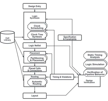
We propose a design flow of SFQ logic circuits as shown in Fig. 5. The design flow is based on that for conventional CMOS circuits. The conventional design flow is adapted to SFQ circuit design. Several dedicated components have been developed to capture design issues of SFQ circuits and
Fig. 5 Design flow for SFQ logic circuits.
integrated in this flow.
A functional description of a circuit is given as the de- sign entry. The description is in circuit schematic or in a description language equivalent to schematic. In Sect. 3, we proposed a new timing-aware description which can be used for logic simulation. Detailed design of the clock distribu- tion network is not required in the design entry.
The design is synthesized into a gate-level logic netlist with the support of dedicated synthesis subsystems for SFQ circuits. Our focus in this stage is the methods for clock dis- tribution. As explained in the previous sections, we design flow-clocking circuits. Because time frames of clock cy-
Fig. 6 Construction of skewed clock distribution network.
cles are different among logic gates, in order to optimize the clock distribution network, we have to solve combinational problems which are hard to solve by hand. Therefore, we developed optimization algorithms to solve the problems.
The netlist is then processed by placement and routing stages. Optimization of the wiring by placement and rout- ing is the key for high-performance circuit design. Timing- driven algorithms are introduced both in the placement and routing stages. It is also necessary to consider geometry in the synthesis stage. For routing design in particular, the it- eration process for optimization is aiming at the timing con- straints in the first place.
Along with the design flow from the design entry to the layout, verification of the circuit, especially the verifica- tion related to the timing, is important. Because the skewed clock design makes the behavior of SFQ logic circuit com- plicated, logical errors in timing are easily introduced in the circuits. In our formal design verification method, we deal with an SFQ circuit as a pipelined circuit with skewed clock for each gate and perform comprehensive verification of the circuit behavior. Circuit simulation explained in Sect. 3.2 is also utilized for verification.
We have developed design tools for SFQ logic circuits, based on the proposed design algorithms. Some of them are implemented as extensions on top of the Cadence Vir- tuoso design environment. The implemented tools includes a clock tree synthesis tool which also perform rough global placement, an automatic PTL routing tool, and a logic sim- ulation tool based on the timing-aware circuit description.
In the following, we look into the algorithms developed for each procedure in the design flow.
4.2 Logical Design
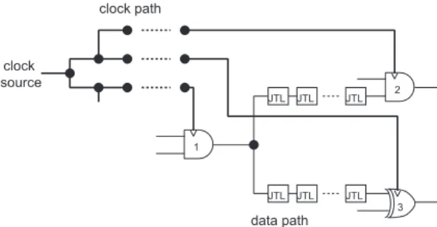
The timing behavior of concurrent-flow clocking SFQ cir- cuits can be regarded as a pipeline constructed for exploiting the ultra-fast switching speed. We have been proposed an al- gorithm for skewed clock scheduling of SFQ logic circuits [9]. We assumed PTLs as the signal wires and showed an al- gorithm to determine the signal timing for each logic gate of a concurrent-flow clocking circuit, with inserting delays on datapaths (Fig. 6). Splitters denoted as black dots in the fig- ure are used for fan-out and JTLs are used as delay elements.
Given a clock period, the proposed algorithm determines the number of splitters on each clock path and delay elements
(JTLs) that should be inserted on each data path, when the clock period can be achieved. Once a clock scheduling is obtained, a clock tree to realize the scheduling can be con- structed. We restricted the solution space to be searched by the proposed algorithm for efficient computation. Experi- mental results on sample circuits showed that the proposed algorithm can obtain near optimal solutions.
As the routability and length of PTLs are not negligi- ble, we have to consider geometry of the clock distribution.
In the method we proposed in [10], a clock tree to distribute clock signals satisfying the timing restrictions for the whole circuit is calculated. A clock tree without wire intersection is obtained. Because the method takes account of geome- try for circuit layout, a linear arrangement of gates in each level is obtained at the same time. This information is to be utilized for the initial placement in the next placement stage.
4.3 Layout Design
Layout design of an SFQ circuit is performed for each log- ical level. Interconnects between adjacent levels can be im- plemented by PTLs. However, using PTLs for short in- terconnects is not efficient, because it requires overheads in timing. Implementing all interconnects by JTLs, on the other hand, is not practical, because the circuit area becomes larger. One reasonable solution is to form clusters of the levels and to use JTLs inside the clusters and PTLs among the clusters. Optimization of the clustering can be done by an algorithm based on dynamic programming, by evaluating the area and delay as the constraint and objective function.
Detailed layout design is done for each logical level or cluster. Using the rough global placement obtained by the clock tree synthesis algorithm, placement of each cell is determined. The constraint comes from the wiring delay and congestion, and the optimization objective is the circuit area.
We have developed a PTL routing method for SFQ cir- cuits based on timing slack allocation [11], [12]. The under- lying routing algorithm is the A∗algorithm which connects two endpoints by heuristic estimation of the wiring cost. In the proposed routing process shown in Fig. 7, clock nets are routed first. Next, we group clocked gates by their level and route data nets for each level. Before the data net routing, we calculate timing slacks and sort wires ordering by tim- ing slack. Each net is routed incrementally in the order of global/detailed routing. The routing and analysis phases are iterated to optimize the layout. Because the timing require- ment is crucial while the routing channel is limited, restric- tions coming from the nets which already have routed are taken into account in the analysis phase. Using timing and layout information of routed nets, timing slack of each path is calculated and the slack is assigned to wire segments com- posing the path. The wire ordering and the congestion map are updated dynamically.
Fig. 7 Algorithm for PTL routing.
4.4 Design Verification
As we have stated before, a concurrent-flow clocking SFQ circuit can be considered as a pipelined circuit. The simula- tion method presented in Sect. 3.2 is effective for verifying the circuit behavior in logic level, because we can deal with both logical and temporal relation of signals by the method.
Another method we have proposed for design verifica- tion is a formal verification method of pipeline processing behavior of SFQ logic circuits [13]. The design is given as a logic circuit netlist with annotated timing information. The specification is given as logic formulae with temporal infor- mation, or as a circuit whose correct operation is guaran- teed. If discrepancies of the behavior are detected, they are fed back to designing process, the circuit design is refined, and verification is performed again.
Because the logic gates are clocked, the verification problem cannot be treated in the same way as the case of combinational circuits. Existing verification methods for se- quential circuits could be applied, but the number of latches, which is equal to the number of clocked logic gates, can be too large and the methods would not be practical. There- fore, we have proposed a dedicated verification method. In the proposed method, verification of circuits are performed in the following two steps.
pipeline timing analysis: We check whether pulses arrive in appropriate clock cycle.
logic sequence verification: We check whether the logical sequence of the circuit satisfies the specification.
Let us see examples of design errors which can be de-
Fig. 8 Circuits with different behavior. (a) A circuit with unclocked CB.
(b) A circuit with clocked OR. (c) A circuit with multiple feedback loop.
tected by the proposed method. Let the circuit to be de- signed is as illustrated in Fig. 8(a). The circuit in Fig. 8(a) implements logical OR operation at pointCusing a conflu- ence buffer (CB). We assume concurrent-flow clocking. Be- cause a CB is not clocked, the CB together with the clocked gates in level 2 can be treated as a single pipeline stage.
Note that a clocked non-inverting buffer gate is equivalent to a D flip-flop. In the design shown in Fig. 8(b), the logical OR operation at pointC is implemented by a clocked OR gate. Though this circuit is similar to the circuit of Fig. 8(a), the implemented logic functions are different because they have different timing behavior. Another design in Fig. 8(c), where the OR gate is driven by clock-follow-data clocking, also has similar circuit structure. A new feedback path is formed in level 2. The logic function is different from that of Fig. 8(b), but can be same as that of 8(a) for a certain initial state.
In order to detect design discrepancy as shown in this example, we deal with the logical structure of the circuit including the timing of pipeline stages. When the circuits contain feedback loops as seen in these examples, the spec- ification described in formulae should contain recurrences.
The input and output variables are common, but the inter- nal variables for the cutpoints of the feedback loops does not necessarily match between two sets of formulae. In this case, we have to check that for all possible sequences of in- put values, output values in each clock cycles of the circuit and those of the specification are identical. It can be proved that checking output values of finite number of clock cy- cles is sufficient to prove the equivalence, and the necessary number of checked clock cycles depends on the length of the feedback loops.
4.5 Circuit Design Using Developed Tools
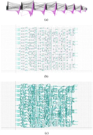
To demonstrate the feasibility of the proposed design flow, we designed an 8-bit Kogge-Stone carry lookahead adder along with the design flow, using the developed tools. The design process is shown in Fig. 9. On a logic design in the schematic view, clock tree synthesis is performed
Fig. 9 Design of a carry lookahead adder. (a) Clock tree synthesis. (b) Placement. (c) Routing.
(Fig. 9(a)). The target frequency is 50 GHz. The 158 logic gates are partitioned into 9 pipeline stages and the gates in each stage are arranged in a row. A clock tree topology and a rough placement of logic gates are obtained. Logic gates are placed (Fig. 9(b)) based on the obtained informa- tion, and then the wires are routed (Fig. 9(c)). The circuit is fabricated using ISTEC advanced process 2 (Fig. 10). The circuit consists of 158 logic cells and 594 PTLs. The num- ber of Josephson junctions is 8397 and the area is 3.9 mm
×3.5 mm. The circuit was fully functional at low speed test, and the partial operation at 50 GHz was confirmed [14], [15].
5. Conclusion
We have been working on design methods for SFQ circuits, and have developed algorithms to cope with design issues specific to SFQ devices. In this paper, we proposed a timing- aware circuit description in logic level and presented a sim- ulation method. Now, we can conclude that we have finally built the fundamental design flow from the design entry in logic level to the physical layout. Our work to integrate the individual algorithms into practical design tools is in progress. Utilization of the timing-aware description to im- prove design process is also included in our future work.
Because the potential of SFQ devices used as logic cir-
Fig. 10 Fabricated Chip of a carry lookahead adder in Fig. 9.
cuits is not yet fully unveiled, alternative ways to employ nonconventional circuit structure will be worth challenging.
One of our approach is a dual-rail asynchronous logic design [16], [17]. Synthesis of asynchronous logic using graph- based logic expression is effective and this method can be applied for small parts such as control units. Another idea is a synthesis method for sequential circuits [18]. Using one- hot encoding and uniform state machine modules, timing design can be made easier. We are also developing a circuit synthesis method based on clockless logic gates which make synchronization using the timing of data pulses.
Acknowledgments
The authors thank Dr. M. Tanaka of Nagoya University for his valuable comments and technical support in detailed de- sign and testing of the circuit. The circuit has been fab- ricated by using ISTEC advanced process 2 (ADP2). The National Institute of Advanced Industrial Science and Tech- nology partially contributed to the circuit fabrication. This work has been supported in part by CREST JST, ALCA JST, and VLSI Design and Education Center (VDEC), the Uni- versity of Tokyo in collaboration with Cadence Design Sys- tems, Inc.
References
[1] K.K. Likharev and V.K. Semenov, “RSFQ logic/memory fam- ily: A new Josephson-junction technology for sub-terahertz-clock- frequency digital systems,” IEEE Trans. Appl. Supercond., vol.1, no.1, pp.3–28, 1991.
[2] T. Satoh, K. Hinode, S. Nagasawa, Y. Kitagawa, M. Hidaka, N. Yoshikawa, H. Akaike, A. Fujimaki, K. Takagi, and N. Takagi,
“Planarization process for fabricating multi-layer Nb integrated cir- cuits incorporating top active layer,” IEEE Trans. Appl. Supercond., vol.19, no.3, pp.167–170, 2009.
[3] Y. Yamanashi, M. Tanaka, A. Akimoto, H. Park, Y. Kamiya, N. Irie, N. Yoshikawa, A. Fujimaki, H. Terai, and Y. Hashimoto, “Design and implementation of a pipelined bit-serial SFQ microprocessor, CORE1β,” IEEE Trans. Appl. Supercond., vol.17, no.2, pp.474–
477, 2007.
[4] H. Park, Y. Yamanashi, K. Taketomi, N. Yoshikawa, M. Tanaka, K.
Obata, Y. Ito, A. Fujimaki, N. Takagi, K. Takagi, and S. Nagasawa,
“Design and implementation and on-chip high-speed test of SFQ half-precision floating-point adders,” IEEE Trans. Appl. Supercond.,
vol.19, no.3, pp.634–639, 2009.
[5] H. Hara, K. Obata, H. Park, Y. Yamanashi, K. Taketomi, N.
Yoshikawa, M. Tanaka, A. Fujimaki, N. Takagi, K. Takagi, and S.
Nagasawa, “Design, implementation and on-chip high-speed test of SFQ half-precision floating-point multiplier,” IEEE Trans. Appl. Su- percond., vol.19, no.3, pp.657–660, 2009.
[6] Y. Kameda, S. Yorozu, and S. Hashimoto, “A new design method- ology for single-flux-quantum logic circuits (SFQ) using passive- transmission-line (PTL) wiring,” IEEE Trans. Appl. Supercond., vol.17, no.2, pp.508–511, 2007.
[7] Y. Yamanashi, T. Kainuma, N. Yoshikawa, I. Kataeva, H. Akaike, A. Fujimaki, M. Tanaka, N. Takagi, S. Nagasawa, and M. Hidaka,
“100 GHz demonstrations based on the single-flux-quantum cell li- brary for the 10 kA/cm2Nb multi-layer process,” IEICE Trans. Elec- tron., vol.E93-C, no.4, pp.440–444, April 2010.
[8] N. Kito, K. Takagi, and N. Takagi, “Timing-aware description meth- ods and gate-level simulation of single flux quantum logic circuits,”
17th Workshop on Synthesis And System Integration of Mixed In- formation technologies (SASIMI2010), R3-5, pp.319–324, 2012.
[9] K. Obata, K. Takagi, and N. Takagi, “A clock scheduling algorithm for high-throughput RSFQ digital circuits,” IEICE Trans. Funda- mentals, vol.E91-A, no.12, pp.3772–3782, Dec. 2008.
[10] K. Takagi, Y. Ito, S. Takeshima, M. Tanaka, and N. Takagi, “Layout- driven skewed clock tree synthesis for superconducting SFQ cir- cuits,” IEICE Trans. Electron., vol.E94-C, no.3, pp.288–295, March 2011.
[11] S. Takeshima, K. Takagi, M. Tanaka, and N. Takagi, “Automated routing method for multi-layered SFQ circuits,” Superconducting SFQ VLSI Workshop (SSV 2009), p.5, 2009.
[12] M. Tanaka, K. Obata, Y. Ito, S. Takeshima, M. Sato, K. Takagi, N. Takagi, H. Akaike, and A. Fujimaki, “Automated passive- transmission-line routing tool for single-flux-quantum circuits based on A* algorithm,” IEICE Trans. Electron., vol.E93-C, no.4, pp.435–
439, April 2010.
[13] K. Takagi, M. Sato, M. Tanaka, and N. Takagi, “A verifica- tion method of pipeline processing behavior of superconducting single-flux-quantum pulse logic circuits,” 16th Workshop on Syn- thesis And System Integration of Mixed Information technologies (SASIMI2010), R2-17, pp.208–213, 2010.
[14] M. Tanaka, S. Takeshima, K. Takagi, H. Akaike, A. Fujimaki, N. Yoshikawa, S. Nagasawa, and N. Takagi, “Multi-layered single- flux-quantum circuits designed using timing-driven automatic rout- ing,” Superconductivity Centennial Conference (SCC 2011), 1-EB- O7, 2011.
[15] M. Tanaka, S. Takeshima, K. Takagi, N. Takagi, and A. Fujimaki,
“Evaluation of 8-bit parallel adder designed using timing-driven automatic router for multi-layered single-flux-quantum circuits,”
IEICE Gen. Conf. 2013, C-8-3, 2013. (in Japanese).
[16] K. Obata, K. Takagi, and N. Takagi, “Design method of dual- rail RSFQ logic circuits using 2×2-join,” IEICE Trans. Electron.
(Japanese Edition), vol.J88-C, no.3, pp.202–209, March 2005.
[17] K. Obata, K. Takagi, and N. Takagi, “Logic synthesis method for dual-rail RSFQ digital circuits using root-shared binary decision di- agrams,” IEICE Trans. Fundamentals, vol.E90-A, no.1, pp.257–266, Jan. 2007.
[18] K. Obata, K. Takagi, and N. Takagi “A method of sequential cir- cuit synthesis using one-hot encoding for single-flux-quantum dig- ital circuits,” IEICE Trans. Electron., vol.E90-C, no.12, pp.2278–
2284, Dec. 2007.
Kazuyoshi Takagi received the B.E., M.E.
and Dr. of Engineering degrees in information science from Kyoto University, Kyoto, Japan, in 1991, 1993 and 1999 respectively. From 1995 to 1999, he was a Research Associate at Nara In- stitute of Science and Technology. He had been an Assistant Professor since 1999 and promoted to an Associate Professor in 2006, at the Depart- ment of Information Engineering, Nagoya Uni- versity, Nagoya, Japan. He moved to Depart- ment of Communications and Computer Engi- neering, Kyoto University in 2011. His current interests include system LSI design and design algorithms.
Nobutaka Kito received the B.E., M.I.S.
and Dr. of Information Science degrees in in- formation engineering from Nagoya University, Nagoya, Japan, in 2004, 2006, and 2009, respec- tively. He was a research associate since 2010 at Kyoto University, Kyoto, Japan. He moved to Chukyo University, Toyota, Japan, as an as- sistant professor in 2012. His current interests include CAD algorithms for single flux quan- tum circuits, design for testability, and computer arithmetic.
Naofumi Takagi received the B.E., M.E., and Ph.D. degrees in information science from Kyoto University, Kyoto, Japan, in 1981, 1983, and 1988, respectively. He joined Kyoto Univer- sity as an instructor in 1984 and was promoted to an associate professor in 1991. He moved to Nagoya University, Nagoya, Japan, in 1994, and promoted to a professor in 1998. He returned to Kyoto University in 2010. His current inter- ests include computer arithmetic, hardware al- gorithms, and logic design. He received Japan IBM Science Award and Sakai Memorial Award of the Information Pro- cessing Society of Japan in 1995, and The Commendation for Science and Technology by the Minister of Education, Culture, Sports, Science and Technology of Japan in 2005.